NaNet: a low-latency NIC enabling GPU-based, real-time low level trigger systems.
Abstract
We implemented the NaNet FPGA-based PCIe Gen2 GbE/APElink NIC, featuring GPUDirect RDMA capabilities and UDP protocol management offloading. NaNet is able to receive a UDP input data stream from its GbE interface and redirect it, without any intermediate buffering or CPU intervention, to the memory of a Fermi/Kepler GPU hosted on the same PCIe bus, provided that the two devices share the same upstream root complex. Synthetic benchmarks for latency and bandwidth are presented. We describe how NaNet can be employed in the prototype of the GPU-based RICH low-level trigger processor of the NA62 CERN experiment, to implement the data link between the TEL62 readout boards and the low level trigger processor. Results for the throughput and latency of the integrated system are presented and discussed.
1 Introduction
The integration of GPUs in trigger and data acquisition systems is currently being investigated in several HEP experiments. At higher trigger levels, when the efficient many-core parallelization of event reconstruction algorithms is possible, the benefit of significantly reducing the number of the farm computing nodes is evident [1, 2]. At lower levels, where tipically severe real-time constraints are present and custom hardware is used, the advantages of GPUs adoption are less straightforward. A pilot project within the CERN NA62 experiment[3] is investigating the usage of GPUs in the central low level trigger processor, exploiting their computing power to implement efficient, high throughput event selection algorithms while retaining the real-time requisites of the system. One of the project preliminary results was that employing commodity NICs and standard software stack caused data transfer over GbE links from readout boards to GPU memories to consume the largest part of the time budget and was the main source of fluctuations in the overall system response time. In order to reduce data transfer latency and its fluctuations, we envisioned the usage of the GPUDirect RDMA technology, injecting readout data directly from the NIC into the GPU memories without any intermediate buffering and the offloading of the network stack protocol management from the CPU, avoiding OS jitter effects. We implemented these two features in the NaNet FPGA-based NIC: the first was inherited from the APEnet+ 3D NIC development [4] while the second was realized integrating an Open IP provided by the FPGA vendor. NaNet NIC currently supports three APElink 34 Gbps channels [5] and one GbE one; a 10GbE version of the design is under development.
After introducing the NA62 multi-level trigger system and motivating the usage of GPUs in its low-level trigger processor, we will provide a description of the NaNet architecture, implementation and performances focusing on its usage as 1 GbE NIC in the case study of the GPU-based L0 trigger processor for the RICH detector.
2 The NA62 multi-level trigger system
The NA62 experiment at CERN [6] has the goal of measuring the Branching Ratio of the ultra-rare decay of the charged Kaon into a pion and a neutrino-antineutrino pair. Due to the very high precision of theoretical prediction on this Branching Ratio, a precise measurement at the level of 100 events would be a stringent test of the Standard Model, also being this Branching Ratio highly sensitive to any new physics particle.
Compared to first observations of this decay [7], the NA62 experiment aims at collecting more events () with a signal to background ratio 10:1, using a novel technique with a high-energy (75 GeV) unseparated hadron beam decaying in flight. The experiment is currently in the final preparation stage, with the first data-taking period foreseen for fall 2014.
The expected Standard Model Branching Ratio is , requiring a very intense beam (main Kaon Branching Ratios is ) and efficient background rejection.
The rate of particle decays reaching the detectors must be reduced by a set of trigger levels down to a rate. The entire trigger chain works on the main digitized data stream [8]. The first level (L0) is implemented in hardware (FPGAs) on the readout boards and performs rather crude and simple cuts on the fastest detectors, reducing the high-rate data stream by a factor 10 to cope with the maximum design rate for event readout of 1 MHz.
Events passing L0 are transferred to the upper trigger levels (L1 and L2) which are software-implemented on a commodity PC farm.
In the standard implementation, the readout boards FPGAs compute simple trigger primitives on the fly, then time-stamp and send them to a central processor for matching and trigger decision. Thus, the maximum latency allowed for the synchronous L0 trigger is related to the maximum data storage time available on the DAQ boards. For NA62 this value is up to 1 ms, in principle allowing use of more compute demanding implementations at this level, i.e. the GPUs.
2.1 The RICH detector low level (L0) trigger
The RICH identifies pions and muons in the momentum range 15 to 35 with a suppression factor better than with good time resolution. Čerenkov light is produced in a 18 m long, 3.7 m wide tube filled with neon at atmospheric pressure. The light is reflected by a composite mirror of 17 m focal length, focused on two separated spots. The two spots are equipped with PMs of 1.8 cm in diameter each. After amplification and discrimination, the PM signal time is digitized by high resolution TDCs. A typical pion ring, for averaged accepted momentum, is identified with firing PMs, as predicted by Monte Carlo and confirmed with a full-length prototype [9]. Time resolution was measured to be better than 100 ps for all momenta in the considered range. Good time resolution and particle identification capability make this detector ideal for use in the trigger system to build stringent conditions.
3 The GPU-based NA62 RICH detector L0 trigger
As a first example of GPU application in the NA62 trigger system we studied the possibility to reconstruct rings in the RICH. The center and the radius of the Čerenkov rings in the detector are related to particle angle/velocity. This information can be employed at trigger level to increase the purity and the rejection power for many triggers of interest. The ring reconstruction could be useful both at L0 and L1. In both cases, because of the high rate of 10 and 1 MHz respectively, the computing power required is significant. The GPUs can offers a simple solution of the problem. The use of video cards in the L1 is straightforward: the GPU can act as “coprocessor” to speed up the processing. On the other hand, the L0 is a low latency synchronous level and feasibility of GPU usage must be verified. To test feasibility and performances, as a starting point we have implemented five algorithms for single ring finding in a sparse matrix of 1000 points (centered on the PMs in the RICH spot) with 20 firing PMs (“hits”) on average.
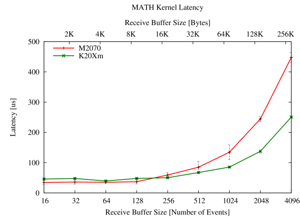
We tested these algorithms on TESLA C1060, C2050, M2070 and K20 [3]. In the following we focus on the fastest algorithm — MATH — where the least-squares method is applied in a coordinate system in which the problem can be analytically solved [10] with a linear inversion. Processing times with input data and results in GPU memory, for the MATH algorithm measured both on TESLA M2070 and K20Xm are plotted in Fig. 2. The contribution of processing to the overall system latency can be kept under control due to the very small fluctuations in GPU kernel execution times.
3.1 Readout - L0 Trigger Processor Data Channel Implementation
Data communication between the TEL62 readout boards and the L0 trigger processor (L0TP) happens over multiple GbE links using UDP streams. The main requisite for the communication system comes from the request for 1 ms and deterministic response latency of the L0TP: communication latency and its fluctuations are to be kept under control. The requisite on bandwidth is 400700 MB/s, depending on the final choice of the primitives data protocol which in turn depends on the amount of preprocessing actually be implemented in the TEL62 FPGA. So in the final system, 46 GbE links will be used to extract primitives data from the readout board towards the L0TP. We studied several options for the implementation of this multiple GbE-based data communication system, benchmarking any of them for a single GbE channel in order to collect indications for the design of the full-fledged system. A first result was that any solution matched the bandwidth specification for a GbE link at significant buffer sizes, so we concentrated on measuring communication latency and, most important in the context of the design of a real-time communication system, latency fluctuations. To perform benchmarks we used two different hardware platforms:
-
•
a Supermicro SuperServer 6016GT-TF with X8DTG-DF motherboard (Intel 5520-Tylersburg chipset), dual Intel Xeon X5570 @2.93 GHz CPU, Intel 82576 GbE and NVIDIA Fermi M2070 GPU (from here on M2070 system)
-
•
a Supermicro SuperServer 7047GR-TPRF with X9DRG-QF motherboard (Intel C602-Patsburg chipset), dual Intel Xeon E5-2609 @2,40 Ghz CPU, Intel i350 GbE and NVIDIA Fermi K20Xm GPU (from here on K20Xm system).
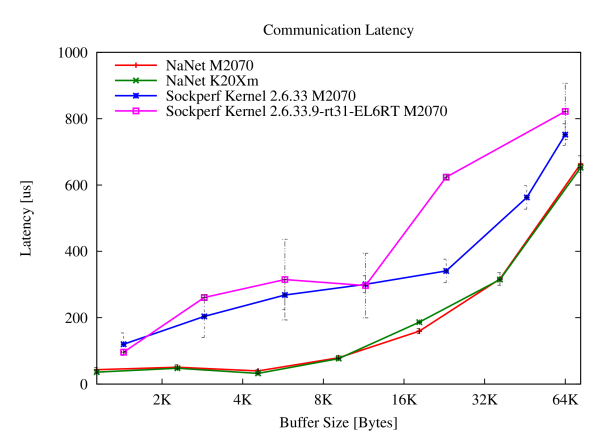
First option considered was a standard Linux installation (CentOS 6.3, Kernel 2.6.33) with integrated GbE interface in the M2070 system; to measure latencies we used the network benchmarking utility sockperf[11]. Results are shown in Fig. 2; at lower buffer sizes latencies are higher than desirable but main drawback of this setup is the great latency variability.
Next option in the attempt of reducing latency fluctuations was trying a real-time kernel on the M2070 system. A great effort has been recently done by OS developers in improving RT features in kernels: predictability in response times, reduced jitters, s accuracy and improved time granularity. In Fig. 2 results obtained with a 2.6.33.9-rt31-EL6RT kernel are plotted; CPUspeed and IRQbalance daemons were stopped and Interrupt moderation was disabled to avoid other possible sources of latency fluctuations. This approach was successful in minimizing fluctuations on latency but increased the latency values up to an incompatible level with the L0TP 1 ms time budget.
Another considered option was usage of PF RING [12], which is a framework for accelerating packet capture implementing a memory-mapped buffer allocated at socket creation, i.e. where incoming packets are copied. PF RING can use either standard drivers or PF RING-aware drivers and works with off-the-shelf GbE NICs. Promising results obtained using this approach are reported and discussed in [13].
Finally, to tackle the real-time requirement of the GPU-based L0TP, we considered reusing the GPUDirect RDMA technology that we already implemented in the APEnet+ project for 3D-torus network card. This led to the design and implementation of the NaNet FPGA-based NIC featuring, besides GPUDirect RDMA capability, a UDP offloading engine. Latency benchmarks obtained using NaNet both in the M2070 and the K20Xm system are shown in 2. Latency and its variability are significantly reduced when compared to other benchmarked solutions. In the following sections we describe the internal architecture of NaNet and report a performance analysis for it and the GPU-based RICH L0TP using NaNet as a communication channel from the readout boards.
4 NaNet
NaNet is an APEnet+ rehaul for real-time data acquisition able to inject directly data from the NIC into the CPU/GPU memory with no intermediate buffering, reusing the APEnet+ GPUDirect RDMA implementation. Moreover, it adds a network stack protocol management offloading engine to the logic to avoid OS jitter effects.
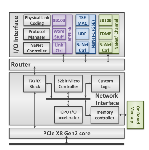
NaNet design supports a configurable number and kind of I/O channels (see figure 4); incoming data streams are processed by a Physical Link Coding block feeding the Data Protocol Manager that in turns extracts the payload data. These payload data are encapsulated in the APEnet+ data packet protocol by the NaNet Controller and sent to the APEnet+ Network Interface, taking care of their delivery to the destination memory.
4.1 NaNet-1 Hardware Architecture
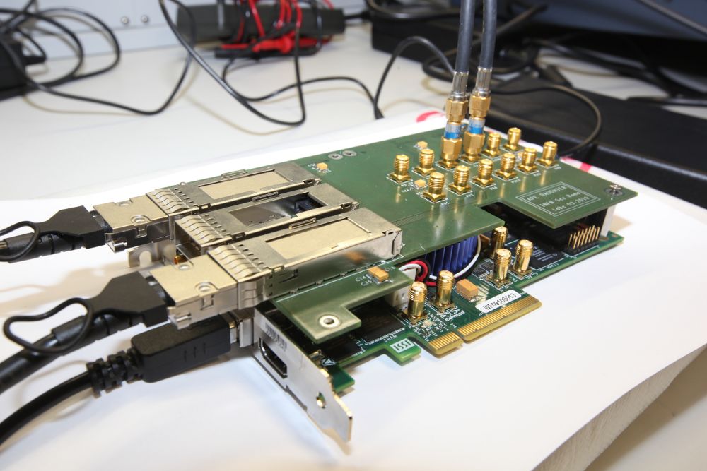
The NaNet-1 is a PCIe Gen2 x8 NIC featuring a standard GbE interface able to directly inject an UDP data stream into the memory of a Fermi- or Kepler-class NVIDIA GPU leveraging on GPUDirect RDMA capabilities, implemented on a Stratix IV GX FPGA Dev Kit. Moreover, it provides 3 bi-directional APElink channels, with the addition of a custom mezzanine equipped with 3 QSFP+ connectors.
The GbE trasmission is designed following the general I/O interface architecture pointed out in figure 4. Physical Link Coding is Altera Triple Speed Ethernet Megacore (TSE MAC), providing 10/100/1000 Mbps Ethernet IP modules. The UDP offloader collects data coming from the TSE MAC, extracting UDP packets payload and providing a 32-bit wide channel achieving 6.4 Gbps, discharging the Nios II from the data protocol management. Finally, the NaNet CTRL is the hardware module in charge of encapsulating the UDP data in the proprietary APEnet+ protocol, parallelizing incoming 32-bit data words into 128-bit APEnet+ ones.
The Network Interface, the packet injection/processing logic providing hardware support for Remote Direct Memory Access (RDMA) protocol for CPU and GPU and the Router with I/O channels multiplexing tasks are inherited from APEnet+.
4.2 NaNet-1 Software Stack
Software components for NaNet-1 operation are needed both on the x86 host and on the Nios II FPGA-embedded controller. On the x86 host, a GNU/Linux kernel driver and an application library are present. The application library provides an API mainly for open/close device operations, registration (i.e. allocation, pinning and returning of virtual addresses of buffers to the application) and deregistration of circular lists of persistent receiving buffers (CLOPs) in GPU and/or host memory and signalling of receive events on these registered buffers to the application (e.g. to invoke a GPU kernel to process data just received in GPU memory). On the controller, a single process application is in charge of device configuration, generation of the destination virtual address inside the CLOP for incoming packets payload and virtual to physical memory address translation performed before the PCIe DMA transaction to the destination buffer takes place.
5 Performance Analysis
We measured NaNet-1 latency and bandwidth using different methods, then we tested it integrated in a simulated GPU-based RICH L0 trigger processor, measuring performances (latency and throughput) of the overall system.
Latency of NaNet-1 NIC was benchmarked using several methods.
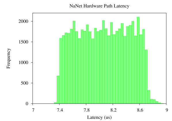
Firstly, we instrumented the FPGA logic with a dedicated hardware path traversal latency measurement system able to add a “profiling” footer to the packet payload, storing up to 4 cycle counters values recorded at different packet processing stages. We were thus able to characterize the latency associated to processing in relevant NaNet-1 subsystems, namely the UDP offloader, the Nios II controller and the Tx block in the Network Interface. In Fig. 6 a histogram is plotted with hardware processing path traversal latency inside NaNet-1: values show an appreciable variability, due to the Nios II controller performing address generation and virtual to physical translation tasks. This clearly indicates the need for a redesign, implementing dedicated FPGA logic blocks performing these two tasks.
A second method was using one of the host GbE ports to send UDP packets according to the NA62 RICH readout data protocol to the NaNet-1 GbE interface: using the x86 TSC register as a common reference time, it was possible in a single process test application to measure latency as time difference between when a received buffer is signalled to the application and the moment before the first UDP packet of a bunch (needed to fill the receive buffer) is sent through the host GbE port. Within this measurement setup (“system loopback”), the latency of the send process is also taken into account. Measurements in Fig. 2 were taken using this method; UDP packets with a payload size of 1168 B (16 events) were sent to a GPU memory receiving buffer of size variable between 1 and 64 UDP packet payload sizes.
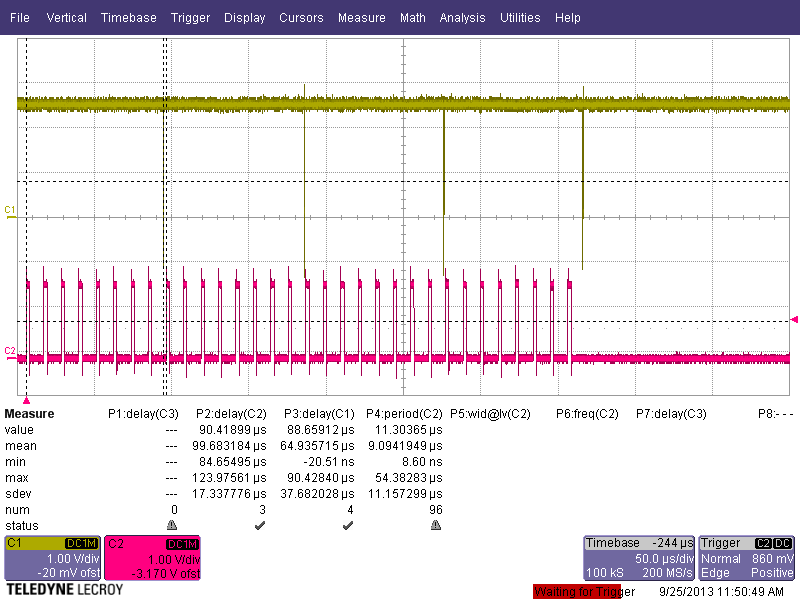
Connecting a TEL62 readout board sending Monte Carlo-generated events stored onto the FPGA through one of its GbE ports to a NaNet-1 board, we were able, besides testing the integration of our NIC in the working environment, to perform oscilloscope latency measurements as depicted in Fig. 6: a bunch of 32 UDP packets is sent from the TEL62 readout board (red signal) and 4 PCIe completion (yellow signal) show the end of the PCIe DMA write transaction towards the GPU memory buffers, each sized 8 times the UDP packet payload size.
As anticipated, bandwidth measurement was also performed, both for the M2070 and the K20Xm system: results are in Fig. 8.
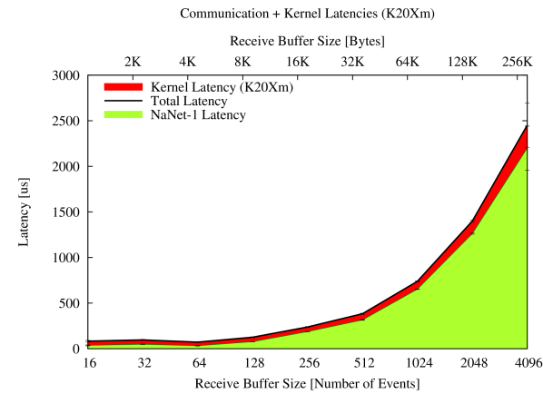
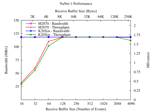
A GPU-based L0TP setup scaled down in bandwidth was reproduced by using a system loopback configuration, with the host system simulating the TEL62 UDP traffic through one of its GbE ports towards a NaNet-1 NIC redirecting incoming data stream towards a GPU memory circular list of receive buffers; once received, such buffers are consumed by a CUDA Kernel implementing the MATH ring-finding algorithm. Communication and kernel processing tasks were serialized in order to perform the measure; these are the results for the K20Xm system in Fig. 8, representing a worst-case situation. During normal operation, this serialization constraint can be relaxed, and kernel processing task overlaps with data communication. Actually this is what has been done to measure system throughput, results are shown in Fig. 8. Combining the two results, we see that using GPU receive buffer sizes ranging from 128 to 1024 events allow the system to remain within the 1 ms time budget while keeping a MEvents/s throughput.
6 Conclusions and Future Work
Our NaNet design proved to be efficient in performing real-time data communication between the NA62 RICH readout system and the GPU-based L0 trigger processor over a single GbE link. These encouraging results are corroborated by benchmarks carried on using one APElink 34 Gbps channel supported by NaNet-1 [14]. To cope with the full system bandwidth requirement we started developing a NaNet design supporting dual 10GbE on SFP+ ports.
Acknowledgment
This work was partially supported by the EU Framework Programme 7 project EURETILE under grant number 247846. G. Lamanna, F. Pantaleo, R. Piandani and M. Sozzi thank the GAP project, partially supported by MIUR under grant RBFR12JF2Z “Futuro in ricerca 2012”; R. Ammendola was supported by MIUR through INFN SUMA project.
References
References
- [1] Clark P J, Jones C, Emeilyanov D, Rovatsou M, Washbrook A and the ATLAS collaboration 2011 Journal of Physics: Conference Series 331 022031 URL http://stacks.iop.org/1742-6596/331/i=2/a=022031
- [2] Rohr D, Gorbunov S, Szostak A, Kretz M, Kollegger T, Breitner T and Alt T 2012 Journal of Physics: Conference Series 396 012044 URL http://stacks.iop.org/1742-6596/396/i=1/a=012044
- [3] Collazuol G, Lamanna G, Pinzino J and Sozzi M S 2012 Nuclear Instruments and Methods in Physics Research A 662 49–54
- [4] Ammendola R et al. 2012 Journal of Physics: Conference Series 396 042059 URL http://stacks.iop.org/1742-6596/396/i=4/a=042059
- [5] Ammendola R et al. 2013 JINST, Journal of Instrumentation, Proceedings of Topical Workshop on Electronics for Particle Physics (TWEPP) 2013 (IOP Publishing) to be published
- [6] Lamanna G 2011 Journal of Physics: Conference Series 335 012071 URL http://stacks.iop.org/1742-6596/335/i=1/a=012071
- [7] Artamonov A V et al. (E949 Collaboration) 2009 Phys. Rev. D 79(9) 092004 URL http://link.aps.org/doi/10.1103/PhysRevD.79.092004
- [8] Avanzini C et al. (for the NA62 Collaboration) 2010 Nucl. Instrum. Methods Phys. Res., A 623 543–545
- [9] Angelucci B et al. 2010 Nucl.Instrum.Meth. A621 205–211
- [10] Crawford J 1983 Nuclear Instruments and Methods in Physics Research 211 223 – 225 ISSN 0167-5087 URL http://www.sciencedirect.com/science/article/pii/0167508783905756
- [11] sockperf http://code.google.com/p/sockperf/
- [12] Deri L 2004 Proceedings of 4th International System Administration and Network Engineering Conference (SANE2004)
- [13] Ammendola R et al. 2013 20th International Conference on Computing in High Energy and Nuclear Physics (CHEP2013) to be published
- [14] Lonardo A et al. 2013 JINST, Journal of Instrumentation, Proceedings of Topical Workshop on Electronics for Particle Physics (TWEPP) 2013 (IOP Publishing) to be published