Defect-induced conductivity anisotropy in MoS2 monolayers
Abstract
Various types of defects in MoS2 monolayers and their influence on the electronic structure and transport properties have been studied using the Density-Functional based Tight-Binding method in conjunction with the Green’s Function approach. Intrinsic defects in MoS2 monolayers significantly affect their electronic properties. Even at low concentration they considerably alter the quantum conductance. While the electron transport is practically isotropic in pristine MoS2, strong anisotropy is observed in the presence of defects. Localized mid-gap states are observed in semiconducting MoS2 that do not contribute to the conductivity but direction-dependent scatter the current, and that the conductivity is strongly reduced across line defects and selected grain boundary models.
I Introduction
The rise of grapheneNovoselov et al. (2005) launched the era of two-dimensional (2D) electronics, the manufacturing of electronic devices on substrates of one or few atomic layers thickness. Graphene shows exceptional mechanical and electronic properties as well as spectacular physical phenomena, as for example massless Dirac fermions.Geim and Novoselov (2007) However, as in 3D electronics, the successful manufacturing of a variety of devices requires the combination of conducting, insulating and semi-conducting materials with tunable properties. One class of 2D semiconductors and semimetals are transition-metal dichalcogenides (TMD). Its most prominent representative, molybdenum disulphide (MoS2), is a direct band gap semiconductor ( = 1.8 eV) in the monolayer (ML) form.Mak et al. (2010); Splendiani et al. (2010); Kuc et al. (2011) Pioneering measurements of MoS2-ML-based devices have shown that at room-temperature the mobility is about 200 cm2 V s-1, when exfoliated onto the HfO2 substrate, however, it decreases down to the 0.1–10 cm2 V s-1 range if deposited on SiO2.Radisavljevic et al. (2011) Various electronic devices have been fabricated on MoS2-ML, including thin film transistors,Radisavljevic et al. (2011); Pu et al. (2012); Kim et al. (2012) logical circuits,Wang et al. (2012) amplifiersRadisavljevic et al. (2012) and photodetectors.Lopez-Sanchez et al. (2013) It has been shown that the electronic properties of MoS2-ML can be easily tuned by doping,Ivanovskaya et al. (2006); Komsa et al. (2012); Dolui et al. (2013) bendingConley et al. (2013) or tube formation,Zibouche et al. (2012); Seifert et al. (2000) tensile strainGhorbani-Asl et al. (2013) or intrinsic defects.Ataca et al. (2011); Zhou et al. (2013); Enyashin et al. (2013); Van der Zande et al. (2013)
The chemical and structural integrity of MoS2 depends on the manufacturing process. Monolayers can be produced, following the top-down approach, from natural MoS2 crystals by micromechanical exfoliation,Mak et al. (2010); Radisavljevic et al. (2011) intercalation based exfoliation,Ramakrishna Matte et al. (2010) or, on larger scale, by liquid-exfoliation techniques.Coleman et al. (2011) On the other hand, chemical vapour deposition (CVD) is a bottom-up procedure and it provides a controllable growth of the material with the desired number of layers on the substrate of interest, e.g. on SiO2Lee et al. (2012) or on graphene.Shi et al. (2012)
MoS2-ML prepared in such different processes may contain numerous defects, including cationic or anionic vacancies, dislocations and grain boundaries. Those defects significantly influence transportLee et al. (2012) and optical propertiesTongay et al. (2013) of these materials. For example, it has been found that the maximum career mobility in CVD MoS2 can be up to 0.02 cm2 V-1 s-1,Lee et al. (2012) while mechanically exfoliated ML showed a mobility of 0.1–10 cm2 V-1 s-1.Novoselov et al. (2005); Radisavljevic et al. (2011) Tongay et al.Tongay et al. (2013) showed that point defects lead to a new photoemission peak and enhancement in photoluminescence intensity of MoS2-ML. These effects were attributed to their trapping potential for free charge carriers and to localized excitons.
Defects may serve as means of engineering the MoS2 properties, similarly as chemical impurities in semiconductor doping. Zhou et al.Zhou et al. (2013) showed that S- and MoS3-vacancies can be generated in CVD MoS2-ML by extended electron irradiation. This suggests that controlled defect-engineering allows tailoring – even locally – the electronic properties of MoS2.
Structural defects in the TMD layers can appear in various types, such as point vacancies, grain boundaries, or topological defects. The point vacancy is one of the native defects which have been investigated both in theoryKomsa et al. (2012); Zhou et al. (2013); Ma et al. (2011); Wei et al. (2012) and experiment.Zhou et al. (2013) The recent experiment by Zhou et al.Zhou et al. (2013) showed that divacancies are only randomly observed, while monovacancies occur more frequently in MoS2-ML. Intrinsic defects can be created without elimination of atoms from the lattice, e.g. by performing Stone-Wales rotations and reconstructing intralayer bonds.Zhou et al. (2013) First principles calculations by Zou et al.Zou et al. (2013) predicted that grain boundaries in MoS2-ML can be formed as odd- or even-fold rings, depending on the rotational angle and stoichiometry, what has been been confirmed in experiment.Van der Zande et al. (2013) Line defects, suggested by Enyashin et al.,Enyashin et al. (2013) introduce a mirror plane into the MoS2-ML, thus forming inversion domains. Yong et al.Yong et al. (2008) showed that a finite atomic line of sulphur vacancies created on a MoS2 surface can behave as a pseudo-ballistic wire for electron transport.
So far, direct measurement of the defect influence on the electronic structure and transport properties have been impossible because of substrate-induced local potential variations and contact resistances. In order to fully understand and exploit defects in MoS2-ML, we study here the electronic properties and the quantum transport of several structural defects using the density-functional based methods. We will show that local defects introduce strongly localized mid-gap states in the electronic structure that act as scattering centers. These scattering states do not open new transport channels, but they introduce high anisotropy in the quantum conductance.
II Methods
All calculations have been carried out using the density-functional based tight-binding (DFTB) methodSeifert et al. (1996); Oliveira et al. (2009) as implemented in the deMonNano code.Koster et al. (2009) The structures of monolayers, that is, atomic positions and lattice vectors, have been fully optimized applying 3D periodic boundary conditions with a vacuum separation of 20 Å perpendicular to the MLs. The DFTB parameters for MoS2-ML have been validated and reported earlier.Seifert et al. (2000); Kaplan-Ashiri et al. (2006)
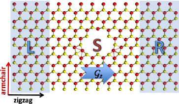
The coherent electronic transport calculations were carried out using the DFTB method in conjunction with the Green’s function (GF) and the Landauer-Büttiker approach.Datta (2005); Di Carlo et al. (2002) Our in-house DFTB-GF software for quantum conductance has already been successfully applied to various nanostructures, including layered and tubular TMDs.Ghorbani-Asl et al. (2013); Miró et al. (2013); Ghorbani-Asl et al. (2013) The transport simulation setup consists of a finite defective MoS2-ML as scattering region, which is connected to two semi-infinite ideal MoS2-ML electrodes (Figure 1). The selected scattering region is at least 28 Å wide in order to prevent direct interaction between the electrodes. The whole system is two-dimensional, and we apply in-plane periodic boundary conditions perpendicular to the transport direction. Thus, unphysical edge effects and out-of-plane periodicity are avoided. Note that the electronic transport through the perfect monolayer represents the result for the bulk conductivity. The quantum conductance () was calculated at zero-bias following the Landauer-Büttiker formula,Landauer (1970) where is represented as:Fisher and Lee (1981)
| (1) |
where denotes the total GF of the scattering region coupled to the electrodes and is the broadening function, self-energies () are calculated following the iterative self-consistent approach.Sancho et al. (1985)
The defective structures are shown in Figure 2. Besides the pristine monolayer (I) we have studied three types of point defects, namely vacancies (II-V and XIII), add-atoms (VI), and Stone-Wales rearrangements (VII-IX). Additionally, we have studied line defects formed from the vacancies (X, XI). In detail, we have considered non-stoichiometric single-atom vacancies of Mo and S atoms (II and III); multiple vacancies with dangling bonds (IV) or with reconstruction towards homonuclear bond formation (V); loops of line defects forming large triangular defects with homonuclear bond formation (XII and XIII). The addition of one MoS2 unit into the lattice (VI) causes rings of different oddity, such as ”4-8” rings, preserving the alternation of chemical bonds. A Stone-Wales rotation of a MoS2 unit by 180∘ (VII and VIII) results in hexagonal rings with homonuclear bonds, while rotation by only 90∘ (IX) forms ”5-7” rings, similar to the ones observed in graphene.Ma et al. (2009) Line defects can be formed by vacancies of S or Mo atoms along zigzag direction (X and XI), resulting in the formation Mo-Mo and S-S dimer bonds, respectively. Such systems have mirror symmetry along the defect lines, what imposes difficulties in the periodic model representation.
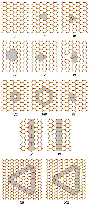
The point defects were simulated using the supercell approach, where the MoS2 ML was expanded to 90 Mo and 180 S atoms. This supercell corresponds to the 59 unit cells of the ideal lattice in rectangular representation. The line defects were optimized using Mo172S344 supercells and, in order to maintain the in-plane 2D periodicity, both types of defects were present simultaneously in the optimization setup. The transport calculations, however, were performed for each line defect separately, keeping the in-plane periodicity perpendicular to the transport direction. Along the transport axis the scattering region was connected to semi-infinite electrodes and the whole system was treated using periodic boundary conditions. Triangular island defects were represented using Mo303S586 and Mo293S606 supercells for S- and Mo-bridges, respectively.
As MoS2-ML are produced under harsh conditions far from thermodynamic equilibrium, it can be assumed that a variety of defects are present in the samples. Thus, we are not considering the thermodynamic stability of the defects, and refer the reader to recent studies on this subject.Enyashin et al. (2013); Enyashin and Ivanovskii (2007) All defects considered in this work are modeled by fully relaxed structures. The geometry optimization did not reveal any considerable distortion of the layers and the defective structures preserved their integrity.
Note that the DFTB method, in the present implementations, does not account for the spin-orbit coupling (SOC) and therefore, this effect has not been considered in the present studies. However, relativistic first-principles calculations including scalar relativistic effects and SO corrections showed that SOC in MoS2-ML accounts for a large valence band splitting of about 145–148 meV, while the conduction band is affected in a much lower degree, by 3 meV band splitting.Zhu et al. (2011); Kormányos et al. (2013) At the same time, the effective masses in the valence change by about 5%, while the effective masses in the conduction band are basically not affected by SOC. The fundamental band gap changes by 50 meV. Thus, the SOC effects will not significantly alter the results that are presented in the remainder of this work.
III Results and Discussion
We have investigated the electronic structure of defective MoS2-ML by calculating orbital-projected densities of state (PDOS). The results were compared with the perfect MoS2 system. Crystal orbitals are visualized corresponding to the states close to the Fermi level (EF) (Figure 3). The electronic structure of MoS2-ML suggests that the bottom of the conduction band is formed from empty Mo-4 orbitals,Enyashin et al. (2013); Kuc et al. (2011) while the top of the valence band is composed of fully occupied and orbitals, in agreement with the crystal-field splitting of trigonal prismatic systems. In pristine MoS2, the highest-occupied and lowest-unoccupied crystal orbitals (HOCO and LUCO) are delocalized and spread homogeneously throughout the system (Figure 2 I). The electronic band gap of MoS2-ML obtained at the DFTB level of about 1.5 eV is smaller than that obtained from DFTMak et al. (2010); Kuc et al. (2011); Splendiani et al. (2010) and experimentMak et al. (2010) due to the deviations in geometry. DFTB-estimated lattice vectors ( = 3.32 Å) are by 5% larger than the experimental values ( = 3.16 Å),Wilson and Yoffe (1969) and, as it has been discussed earlier, such a distortion in geometry causes the decrease in the band gap.Ghorbani-Asl et al. (2013) However, these discrepancies should not alter general trends and conclusions drawn here, as the relative change in the electronic structure is not influenced.
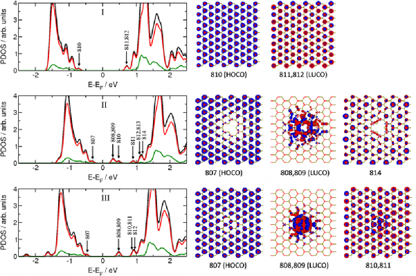
As known from the literature,Komsa et al. (2012); Zhou et al. (2013) defects result in significant changes of the electronic structure close to EF and introduce mid-gap states. The mid-gap states are strongly localized in the vicinity of the defects and are mostly of 4-Mo type, thus they act as scattering centers. Although defect states reduce the band gap significantly, the scattering character will prevent opening any new conduction channels close to EF.
In case of a single Mo vacancy (Figure 3 II), the valence band maximum (HOCO) resembles the characteristics of perfect MoS2-ML, while the edge of conduction band is formed by two individual mid-gap states (states 808/809 and 810 in Figure 3 II), the first being the LUCO. The next delocalized states are located at around 1.2 eV above EF (state 814). A similar situation is observed for the single S vacancy (Figure 3 III), with the LUCO (degenerated states 808/809) composed of single strongly localized states. In this case, the next delocalized states are present only at about 1 eV above EF (810/811).
For larger point defects, where both types of elements are removed from the lattice, the electronic structure changes even stronger, with HOCO states being no longer delocalized. In the case of Stone-Wales defects, the band gap reduces with the number of rotated bonds and introduces a larger number of mid-gap states. At the same time, the HOCO becomes more localized (Figure S1 and S2 in Supporting Information).SI
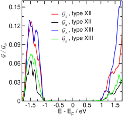
Considering the triangular domain structures (XII and XIII), which contain Mo-Mo and S-S line defects, the PDOS shows interesting characteristics.Enyashin et al. (2013) The Mo-Mo bridges contribute primary with the 4 to the HOCO and the LUCO. These are localized states at about 2.5 eV below EF, indicating the formation of strong MoMo bonds. In contrast, the S-S line defects form S-3 states, which do not contribute to the PDOS close to EF. These states can be found deep in the valence band region at about 3 eV below EF. The states in the vicinity of EF are, therefore, composed exclusively from the edge states of the MoS2 domains.
The defect-induced variations in the electronic structure affect the electronic transport in the MoS2-ML. The transport through MoS2 should be direction dependent due to the structural anisotropy of the system. The pristine layer shows, however, very little anisotropy in the electron conductivity as reported earlier.Ghorbani-Asl et al. (2013)
The two extremes are transport along armchair () or zigzag () directions. In order to ensure transferability of the results, we used a supercell with almost equal length and width along both transport directions (La = 28.75 Å and Lz = 29.88 Å).
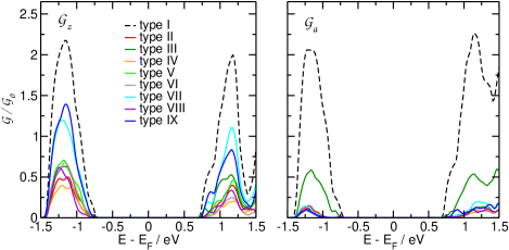
Figure 4 shows the electron conductivity of the MoS2-ML in the pristine form and in the presence of various point defects along the armchair and zigzag directions. The occurrence of defects reduces the conductivity (transmittance) in comparison with the pristine layer at 1.2 eV below and above EF. This is expected as the vacancy causes backscattering effects,Rutter et al. (2007); Deretzis et al. (2010) and, not surprisingly, the conductivity depends strongly on the type and concentration of the point defects. Noteworthy, in contrast to the pristine ML, the electron conductivity of the defective systems becomes strongly direction dependent and the conductivity is suppressed much stronger along the armchair direction. The only exception is the single S-vacancy, where the transport is rather direction independent.
The directional dependence of the conductance might arise from different transmission pathwaysWang et al. (2009); Liu et al. (2013) and electron hopping within defective parts of MoS2-ML.Remskar et al. (2011) To date, only grain boundaries have been studied in experiment, and our results are consistent with the results reported by the Heinz group.Van der Zande et al. (2013)
In case of transport in armchair direction, the electron conductance of MoS2 with one Mo-vacancy, corresponding to 1.11% structural defects, is suppressed by 75% compared with the pristine layer. The single S vacancy (0.55% structural defects) shows higher electron conductivity due to the electron injection directly to the conduction band. For the Stone-Wales defects (VII and IX) the conductance is reduced by less than 50% with respect to the pristine structure.
Figure 5 shows the transport properties of the MoS2-ML with triangular grain boundaries along the armchair and zigzag directions. It is very interesting to notice that in this case does not depend on the type of the defect and similar values are obtained for Mo–Mo and S–S bridges. The conductance is, however, strongly direction-dependent and again we observe that along the armchair lines it is more suppressed than along the zigzag ones.
Our results indicate that local defects introduce spurious minor conductance peaks close to EF (see Figure S3 in Supporting InformationSI ). Because these electronic states are strongly localized, they do not contribute to the overall quantum transport, as they cannot generate additional conducting channels for a specific energy window within the perfect semi-infinite electrodes.
We have also studied the conductance across line defects (X, XI) with respect to the length of the scattering region ls (see Figure 6). In this case, the structure is periodic along the line defects but in the perpendicular direction there is a mirror symmetry, which should be considered in the transport simulations and the choice of the electrodes. Here, our electrodes are still perfect MoS2-MLs, but represent mirror images with respect to each other. Therefore, we have decided to vary the length of ls and investigate its influence on the transport properties.
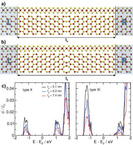
Our results show that the conductance at about +/-1.5 eV from the Fermi level reduces with increasing the channel length, however the band gap does not change and no open channels are present close to the EF.
IV Conclusion
In summary, we investigated the coherent electron transport through MoS2-ML with various defects on the basis of the Green’s functions technique and the DFTB method. The presence of local defects leads to the occurrence of mid-gap states in semiconducting MoS2-ML. These states are localized and act as scattering centers. Our transport calculations show that single-atomic vacancies can significantly reduce the average conductance. The decrease of conductance depends on the type and concentration of the defects, and, surprisingly, on the transport direction. We find significant anisotropy of electron transfer in MoS2-ML with grain boundaries. Since structural and electronic properties of layered semiconducting TMD are comparable, we expect similar effects to occur in other defective TMD-ML. Our results indicate that structural defects and grain boundaries are principal contributors to the electronic transport properties of MoS2 monolayers, thus rationalizing the large variation of electronic conductivity in different samples.
V Acknowledgements
This work was supported by Deutsche Forschungsgemeinschaft (HE 3543/18-1), the Office of Naval Research Global (Award No N62909-13-1-N222) the European Commission (FP7-PEOPLE-2009-IAPP QUASINANO, GA 251149, and FP7-PEOPLE-2012-ITN MoWSeS, GA 317451) and ERC project (INTIF 226639).
References
- Novoselov et al. (2005) Novoselov, K. S.; Jiang, D.; Schedin, F.; Booth, T. J.; Khotkevich, V. V.; Morozov, S. V.; Geim, A. K. Proc. Nat. Acad. Sci. USA 2005, 102, 10451–10453.
- Geim and Novoselov (2007) Geim, A. K.; Novoselov, K. S. Nat. Mater. 2007, 6, 183–191.
- Mak et al. (2010) Mak, K. F.; Lee, C.; Hone, J.; Shan, J.; Heinz, T. F. Phys. Rev. Lett. 2010, 105, 136805–1–136805–4.
- Splendiani et al. (2010) Splendiani, A.; Sun, L.; Zhang, Y. B.; Li, T. S.; Kim, J.; Chim, C. Y.; Galli, G.; Wang, F. Nano Lett. 2010, 10, 1271–1275.
- Kuc et al. (2011) Kuc, A.; Zibouche, N.; Heine, T. Phys. Rev. B 2011, 83, 245213–1–245213–4.
- Radisavljevic et al. (2011) Radisavljevic, B.; Radenovic, A.; Brivio, J.; Giacometti, V.; Kis, A. Nat. Nanotechnol. 2011, 6, 147–150.
- Pu et al. (2012) Pu, J.; Yomogida, Y.; Liu, K.-K.; Li, L.-J.; Iwasa, Y.; Takenobu, T. Nano Lett. 2012, 12, 4013–4017.
- Kim et al. (2012) Kim, S.; Konar, A.; Hwang, W.-S.; Lee, J. H.; Lee, J.; Yang, J.; Jung, C.; Kim, H. s.; Yoo, J.-B.; Choi, J.-Y.; Jin, Y. W.; Lee, S. Y.; Jena, D.; Choi, W.; Kim, K. Nat. Commun. 2012, 3, 1011–1–1011–7.
- Wang et al. (2012) Wang, H.; Yu, L.; Lee, Y.-H.; Shi, Y.; Hsu, A.; Chin, M. L.; Li, L.-J.; Dubey, M.; Kong, J. g.; Palacios, T. Nano Lett. 2012, 12, 4674–4680.
- Radisavljevic et al. (2012) Radisavljevic, B.; Whitwick, M. B.; Kis, A. Appl. Phys. Lett. 2012, 101, 043103–1–043103–4.
- Lopez-Sanchez et al. (2013) Lopez-Sanchez, O.; Lembke, D.; Kayci, M.; Radenovic, A.; Kis, A. Nat. Nanotechnol. 2013, 8, 497–501.
- Ivanovskaya et al. (2006) Ivanovskaya, V. V.; Seifert, G.; Ivanovskii, A. L. Russ. J. Inorg. Chem. 2006, 51, 320–324.
- Komsa et al. (2012) Komsa, H.-P.; Kotakoski, J.; Kurasch, S.; Lehtinen, O.; Kaiser, U.; Krasheninnikov, A. V. Phys. Rev. Lett. 2012, 109, 35503–1–035503–5.
- Dolui et al. (2013) Dolui, K.; Rungger, I.; Sanvito, S. Phys. Rev. B 2013, 87, 165402–1–165402–7.
- Conley et al. (2013) Conley, H. J.; Wang, B.; Ziegler, J. I.; Haglund, R. F., Jr.; Pantelides, S. T.; Bolotin, K. I. Nano Letters 2013, 13, 3626–3630.
- Zibouche et al. (2012) Zibouche, N.; Kuc, A.; Heine, T. Eur. Phys. J. B 2012, 85, 1–7.
- Seifert et al. (2000) Seifert, G.; Terrones, H.; Terrones, M.; Jungnickel, G.; Frauenheim, T. Phys. Rev. Lett. 2000, 85, 146–149.
- Ghorbani-Asl et al. (2013) Ghorbani-Asl, M.; Borini, S.; Kuc, A.; Heine, T. Phys. Rev. B 2013, 87, 235434–1–235434–6.
- Ataca et al. (2011) Ataca, C.; Sahin, H.; Akturk, E.; Ciraci, S. J. Phys. Chem. C 2011, 115, 3934–3941.
- Zhou et al. (2013) Zhou, W.; Zou, X.; Najmaei, S.; Liu, Z.; Shi, Y.; Kong, J.; Lou, J.; Ajayan, P. M.; Yakobson, B. I.; Idrobo, J.-C. Nano Lett. 2013, 13, 2615–2622.
- Enyashin et al. (2013) Enyashin, A. N.; Bar-Sadan, M.; Houben, L.; Seifert, G. J. Phys. Chem. C 2013, 117, 10842–10848.
- Van der Zande et al. (2013) Van der Zande, A. M.; Huang, P. Y.; Chenet, D. A.; Berkelbach, T. C.; You, Y.; Lee, G.-H.; Heinz, T. F.; Reichman, D. R.; Muller, D. A.; Hone, J. C. Nat. Mater. 2013, 12, 554–561.
- Ramakrishna Matte et al. (2010) Ramakrishna Matte, H. S. S.; Gomathi, A.; Manna, A. K.; Late, D. J.; Datta, R.; Pati, S. K.; Rao, C. N. R. Angew. Chem. Int. Edit. 2010, 49, 4059–4062.
- Coleman et al. (2011) Coleman, J. N.; Lotya, M.; O’Neill, A.; Bergin, S. D.; King, P. J.; Khan, U.; Young, K.; Gaucher, A.; De, S.; Smith, R. J.; Shvets, I. V.; Arora, s. K.; Stanton, G.; Kim, H.-Y.; Lee, K.; Kim, G. T.; Duesberg, G. S.; Hallam, T.; Boland, J. J.; Wang, J. J.; Do negan, J. F.; Grunlan, J. C.; Moriarty, G.; Shmeliov, A.; Nicholls, R. J.; Perkins, J. M.; Grieveson, E. M.; Theuwissen, K.; McComb, P. D., D W an d Nellist; Nicolosi, V. Science 2011, 331, 568–571.
- Lee et al. (2012) Lee, Y.-H.; Zhang, X.-Q.; Zhang, W.; Chang, M.-T.; Lin, C.-T.; Chang, K.-D.; Yu, Y.-C.; Wang, J. T. s.-W.; Chang, C.-S.; Li, L.-J.; Lin, T.-W. Adv. Mater. 2012, 24, 2320–2325.
- Shi et al. (2012) Shi, Y.; Zhou, W.; Lu, A.-Y.; Fang, W.; Lee, Y.-H.; Hsu, A. L.; Kim, S. M.; Kim, K. K.; Yang, H. Y.; Li, L.-J.; Idrobo, J.-C.; Kong, J. Nano Lett. 2012, 12, 2784–2791.
- Tongay et al. (2013) Tongay, S.; Suh, J.; Ataca, C.; Fan, W.; Luce, A.; Kang, J. S.; Liu, J.; Ko, R., Changhyun a nd Raghunathanan; Zhou, J.; Ogletree, F.; Li, J.; Grossman, J. C.; Wu, J. Sci. Rep. 2013, 3, 2657–1–2657–5.
- Zhou et al. (2013) Zhou, Y.; Yang, P.; Zu, H.; Gao, F.; Zu, X. Phys. Chem. Chem. Phys. 2013, 15, 10385–10394.
- Ma et al. (2011) Ma, Y.; Dai, Y.; Guo, M.; Niu, C.; Lu, J.; Huang, B. Phys. Chem. Chem. Phys. 2011, 13, 15546–15553.
- Wei et al. (2012) Wei, J.; Ma, Z.; Zeng, H.; Wang, Z.; Wei, Q.; Peng, P. AIP adv. 2012, 2, 042141–1–042141–7.
- Zou et al. (2013) Zou, X.; Liu, Y.; Yakobson, B. I. Nano Lett. 2013, 13, 253–258.
- Yong et al. (2008) Yong, K. S.; Otalvaro, D. M.; Duchemin, I.; Saeys, M.; Joachim, C. Phys. Rev. B 2008, 77, 205429–1–205429–9.
- Seifert et al. (1996) Seifert, G.; Porezag, D.; Frauenheim, T. Int. J. Quantum Chem. 1996, 58, 185–192.
- Oliveira et al. (2009) Oliveira, A. F.; Seifert, G.; Heine, T.; Duarte, H. A. J. Br. Chem. Soc. 2009, 20, 1193–1205.
- Koster et al. (2009) Koster, A. M.; Flores, R.; Geudtner, G.; Goursot, A.; Heine, T.; Patchkovskii, S.; Reveles, J. U.; Vela, A.; Salahub, D. R. deMonNano. deMonNano, Jabobs University Bremen, http://physics.jacobs-university.de/theine/research/deMon, 2009.
- Kaplan-Ashiri et al. (2006) Kaplan-Ashiri, I.; Cohen, S. R.; Gartsman, K.; Rosentsveig, R.; Ivanovskaya, V. V.; Heine, T.; Seifert, G.; Wagner, H. D.; Tenne, R. Proc. Natl. Acad. Sci. USA 2006, 103, 523–528.
- Datta (2005) Datta, S. Quantum Transport: Atom to Transistor, 2nd ed.; Cambridge University Press: New York, 2005.
- Di Carlo et al. (2002) Di Carlo, A.; Gheorghe, M.; Lugli, P.; Sternberg, M.; Seifert, G.; Frauenheim, T. Physica B 2002, 314, 86–90.
- Miró et al. (2013) Miró, P.; Ghorbani-Asl, M.; Heine, T. Adv. Mater. 2013, 25, 5473–5475.
- Ghorbani-Asl et al. (2013) Ghorbani-Asl, M.; Zibouche, N.; Wahiduzzaman, M.; Oliveira, A. F.; Kuc, A.; Heine, T. Sci. Rep. 2013, 3, 2961–1–2961–8.
- Landauer (1970) Landauer, R. Philos. Mag. 1970, 21, 863–867.
- Fisher and Lee (1981) Fisher, D. S.; Lee, P. A. Phys. Rev. B 1981, 23, 6851.
- Sancho et al. (1985) Sancho, M. P. L.; Sancho, J. M. L.; Sancho, J. M. L.; Rubio, J. J. Phys. F., Met. Phys. 1985, 15, 851–858.
- Ma et al. (2009) Ma, J.; Alfè, D.; Michaelides, A.; Wang, E. Phys. Rev. B 2009, 80, 33407–1–033407–4.
- Enyashin and Ivanovskii (2007) Enyashin, A. N.; Ivanovskii, A. L. Semiconductors 2007, 41, 81–86.
- Zhu et al. (2011) Zhu, Z. Y.; Cheng, Y. C.; Schwingenschlögl, U. Phys. Rev. B 2011, 84, 153402.
- Kormányos et al. (2013) Kormányos, A.; Zólyomi, V.; Drummond, N. D.; Rakyta, P.; Burkard, G.; Fal’ko, V. I. Phys. Rev. B 2013, 88, 045416.
- Wilson and Yoffe (1969) Wilson, J. A.; Yoffe, A. D. Adv. Phys. 1969, 18, 193–335.
- (49) See EPAPS Document No. [] for the projected densities of states of MoS2-MLs with larger point and grain boundary defects (structures IV-IX), and their detailed electron conductance close to the Fermi level.
- Rutter et al. (2007) Rutter, G. M.; Crain, J. N.; Guisinger, N. P.; Li, T.; First, P. N.; Stroscio, J. A. Science 2007, 317, 219–222.
- Deretzis et al. (2010) Deretzis, I.; Fiori, G.; Iannaccone, G.; La Magna, A. Phys. Rev. B 2010, 81, 85427–1–85427–5.
- Wang et al. (2009) Wang, N.; Liu, H.; Zhao, J.; Cui, Y.; Xu, Z.; Ye, Y.; Kiguchi, M.; Murakoshi, K. J Phys. Chem. C 2009, 113, 7416–7423.
- Liu et al. (2013) Liu, H.; Wang, H.; Zhao, J.; Kiguchi, M. J. Comput. Chem. 2013, 34, 360–365.
- Remskar et al. (2011) Remskar, M.; Mrzel, A.; Virsek, M.; Godec, M.; Krause, M.; Kolitsch, A.; Singh, A.; Seabaugh, A. Nanoscale Res. Lett. 2011, 6, 26–1–26–6.