Plasmons in metallic mono- and bilayer transition metal dichalcogenides
Abstract
We study the collective electronic excitations in metallic single- and bilayer transition metal dichalcogenides (TMDCs) using time dependent density functional theory in the random phase approximation. For very small momentum transfers (below Å-1) the plasmon dispersion follows the behavior expected for free electrons in two dimensions. For larger momentum transfer the plasmon energy is significantly red shifted due to screening by interband transitions. At around Å-1 the plasmon enters the dissipative electron-hole continuum and the plasmon dispersions flatten out at an energy around 0.6-1.1 eV, depending on the material. Using bilayer NbSe2 as example, we show that the plasmon modes of a bilayer structure take the form of symmetric and anti-symmetric hybrids of the single-layer modes. The spatially anti-symmetric mode is rather weak with a linear dispersion tending to zero for while the energy of the symmetric mode follows the single-layer mode dispersion with a slight blue shift.
I Introduction
The success of graphene research has created a surge in interest for other types of atomically thin two-dimensional (2D) materials.Britnell et al. (2012); Wang et al. (2012). A particularly interesting class of 2D materials are the transition metal dichalcogenides (TMDC) whose electronic properties range from semiconducting to metallic and even superconducting. In combination with graphene and 2D insulators like hexagonal boron-nitride, the TMDCs could form the basis for artificially layered van der Waals structures with tailored electronic properties. While monolayers of semiconducting TMDCs have been fabricated and studied quite extensivelyRadisavljedic et al. (2011); Mak et al. (2010); Splendiani et al. (2010), metallic TMDCs have received less attention, possible due to stability issuesgeim . However, exfoliation of atomically thin layers of TaSe2, TaS2, and NbSe2 have been reportedcastellanos ; ayari ; staley .
The optical properties of a metallic system are to large extent governed by the collective excitations known as plasmons. In (doped) graphene, it was demonstrated that the energy of the so-called metallic plasmon, which is formed by intraband transitions within the or bands, can be varied by electrostatic gating or nanostructuring. Furthermore, the plasmons facilitates a strong spatial confinement of light making graphene interesting for applications within plasmonicsJu et al. (2011); Chen et al. (2012). However, the energy of the metallic plasmon is restricted by the achievable carrier concentration and this limits applications of graphene plasmonics to the tetrahertz regime. Metallic TMDCs have much higher charge carrier densities leading to plasmon energies of around 1 eV in bulk TMDCsliang ; König et al. (2012); Cudazzo et al. (2012); Faraggi et al. (2012). Together with the possibility of tuning the plasmon energies and lifetimes through quantum confinement or plasmon hybridizationProdan et al. (2003); Wang et al. (2007), this makes few-layer TMDCs interesting candidates for nano-plasmonic applications in the optical frequency regime. We mention that the efficient coupling of 2D plasmons and light generally requires some kind of scattering of the light to overcome the momentum mismatchmortensen .
First-principles calculations of the loss spectrum of several single- and bilayer TMDCs was recently reported in Ref. johari, . While these calculations revealed the energy of the and interband plasmons they did not address the nature of the intraband plasmons of the metallic systems which are only seen for finite due to the dispersion in the small limit.
In this paper we study the intraband plasmons in monolayers of six different metallic TMDCs using first-principles calculations. For very small momentum transfer ( Å), the plasmon energy follows the classical behavior of free electrons in 2D. At larger the plasmons become screened by interband transitions leading to significant redshift compared to the free electron result, and the plasmon dispersions flatten out at an energy in the range 0.6-1.1 eV, depending on the material. At around Å-1, the plasmon enters the dissipative region of interband transitions and the plasmons acquire a finite lifetime. Using a recently developed method for visualizing the induced density associated with a plasmon mode, we study how the single layer plasmons hybridize to form a symmetric and a (weak) anti-symmetric plasmon in a bilayer structure. The symmetric mode of the bilayer is slightly blue shifted relative to the single-layer plasmon. This pushes it closer towards the dissipative interband continuum and reduces its strength compared to the single-layer plasmon.
II Method
All density functional theory (DFT) calculations have been performed with the GPAW electronic structure codeEnkovaara et al. (2010). We study single layers of TMDCs with the chemical form , where belongs to the group transition metals , and and the chalcogen is either or , which results in six different combinations. The layers were modeled within a periodic supercells with Å of vacuum separating the periodic images in the perpendicular direction. The structures were relaxed with the Perdew-Burke-Ernzerhof (PBE) exchange-correlation functionalpbe . The single-particle states used to construct the response function were calculated using the orbital-dependent GLLBSC (Gritsenko, Leeuwen, Lenthe, and Baerends potentialgritsenko with the modifications from Kuisma et al.Kuisma et al. (2010)) functional which has been shown to give accurate band energies of semiconductors. In the context of plasmons, correct band positions are important to describe the onset of interband transitions correctly. The 2D Brillouin zone (BZ) was sampled using k-points for most calculations while a dense grid of was used in order to study very small momentum transfers.
The dielectric matrix for in-plane wave vectors was calculated in the random phase approximation (RPA)bohm_pines following the implementation of Ref. Yan et al., 2011
| (1) |
For the reciprocal lattice vectors and we used a cutoff of 50 eV to account for local field effects, and empty states up to 30 eV above the Fermi level were included in the non-interacting response function matrix . We have checked that the plasmon energies are well converged (to within 0.1 eV) with these parameters. We note that inclusion of the ALDA kernel was found to have negligible effect on the loss spectrum of bulk NbSe2Cudazzo et al. (2012), and based on this we expect the RPA to be valid also for the 2D TMDCs studied here. In order to remove the interaction between supercells, the Coulomb interaction was truncated in the direction perpendicular to the layersRozzi et al. (2006). If this is not done the plasmons in neighboring layers will interact for in-plane wave vectors , where is the distance between the layers. In particular the plasmon energy will incorrectly tend to a finite energy in the limit.
The electron energy loss spectrum (EELS) was calculated from the inverse of the macroscopic dielectric function, :
| (2) |
The plasmon energies are obtained as the peaks in the loss spectrum which is calculated for different momentum transfers parallel to the layer, , and the integrated weight of the loss peaks is used as a measure of the strength of the plasmon mode.
II.1 Plasmon eigenmodes
A simple method to identify and compute the plasmon modes of a metallic nanostructure was introduced in Ref. Andersen et al., 2012. In the present work, the method has been used to analyze the plasmon excitations of the bilayer structure. An outline of the method is given below.
A self-sustained charge density oscillation, , can exist in a material if the related potential, satisfying Poisson s equation , obeys the equation
| (3) |
This corresponds to the case of having a finite induced potential in the absence of an external potential, which is the criterion for the existence of a plasmon. In general, this equation cannot be exactly satisfied due to a finite imaginary part originating from single-particle transitions, which will lead to damping of the charge oscillation. When the damping in the material is small, it is sufficient to require only that the real part of vanishes and use the following definition for the potential associated with a plasmon mode of frequency :
| (4) |
where is a real number. The plasmon modes are thus eigenfunctions corresponding to purely imaginary eigenvalues of the dielectric function. Physically, they represent the potential associated with self-sustained charge-density oscillations damped by electron-hole pair formations at the rate . The right-hand-side eigenfunctions, , define the induced potential of the eigenmodes, and the corresponding induced density can be obtained as the left-hand-side (dual) eigenfunctions of the dielectric functionAndersen et al. (2012). In the case of larger and frequency-dependent damping, a more accurate approach is to use the eigenvalues of , denoted , and use the criterion
| (5) |
to define a plasmon mode. This definition takes into account that a finite imaginary part of may shift the plasmon peaks in the loss spectrum away from the zeros of .
In contrast to the standard definition of the loss spectrum, Eq. (2), which measures the energy loss of a plane wave perturbation, the definition (5) provides a resolution of the loss spectrum into the intrinsic plasmon eigenmodes of the system. As a simple example we mention the resolution of the loss spectrum of a thin metal film into bulk and surface modesAndersen et al. (2012).
In practice, the plasmon eigenmodes are obtained by diagonalizing the dynamical dielectric function (in the and basis) for each point on a frequency grid. The dielectric eigenvalue spectrum results in a set of distinct eigenvalue curves that evolves smoothly with energy, each curve corresponding to a separate plasmon eigenmode, see Fig. 4 (left panel).
III Results
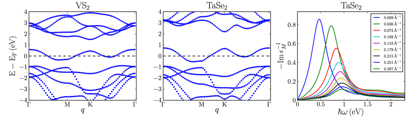
In the left panels of Fig. 1 we show the band structures for VS2 and TaSe2 obtained with the GLLBSC functional. We note that the band structures obtained with PBE are quite similar. Compared to semiconducting TMDCs such as , the reduced -state occupation of the transition metal leads to a half-filled band. From the band structure plotted in Fig. 1 along the high symmetry direction it can be seen that the metallic band crosses the Fermi level along two curves in the 2D Brillouin zone. The band is situated in a gap of approximately 2.5-3 eV and stems from hybridization of the -state of the transition metal with the vertical orbitals of the chalcogen. The band structures of the six materials are very similar, showing only minor variations in the width of the metallic band, and details in the position of the fully occupied or unoccupied bands. A comprehensive study of the electronic structure of several 2D TMDCs was reported in ataca, .
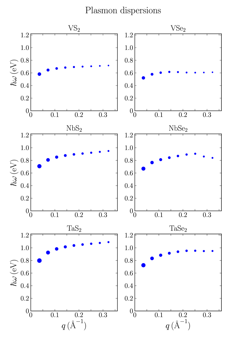
An example of an electron energy loss spectrum is shown in Fig. 1, here calculated for for momentum transfers in the direction. Momentum transfers along and was found to produce very similar results. The pronounced peaks in the loss spectrum are due to plasmon excitations. The plasmon dispersions of the six TMDCs are shown in Fig. 2, where the strength of the resonances is indicated by the size of the markers. In general, higher plasmon energies (for fixed momentum transfer) are found for the TMDCs with heavier transition metal ions. On the other hand, the TMDCs containing heavier species have larger lattice constants and thus lower density of free charge carriers. The trend in plasmon energy is therefore opposite to the free electron model wich predicts the plasmon energy to scale with the charge density as . As we show below, the TMDC plasmon dispersions deviate from the 2D free-electron model due to (i) the non-parabolic shape of the metallic band, and (ii) screening by interband transitions. We note that the -behavior of 2D free-electron plasmons in the small limit is not directly seen from the figure. This is simply because the applied -point grid is not fine enough to reveal this behavior around (this is evident from Fig. 3 where a finer -point mesh was used). We mention that crystal local field effects within the plane may be a third reason for deviations with the 2D free-electron model. However, the homogeneous nature of the 2D TMDC suggests that this will be a rather weak effect.
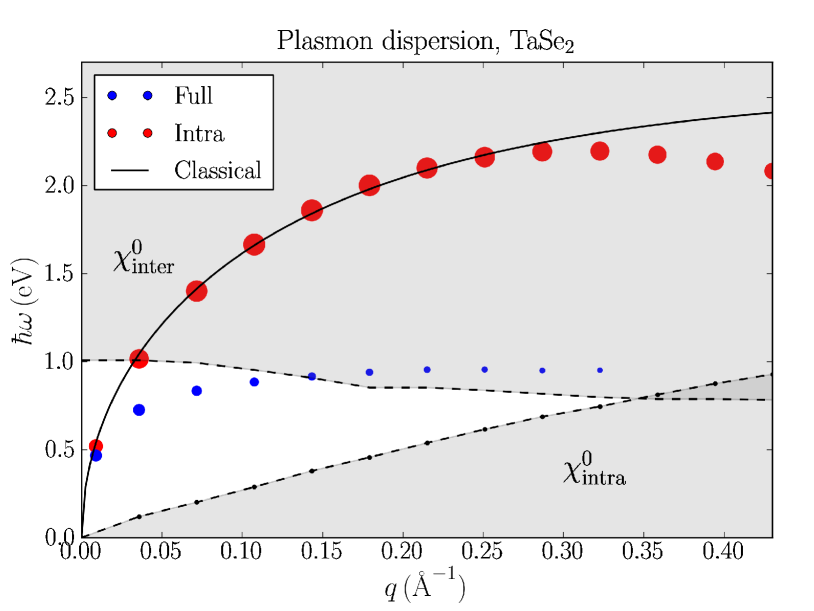
To investigate the origin of the deviation from free-electron behavior we have studied the separate effects of intra- and interband transitions on the plasmon resonances of mono-layer . The non-interacting density response function can be divided into two contributions:
| (6) |
where the first term is obtained by only including transitions within the metallic band in the response calculation, and the second term by including all transitions between separate bands. When the dielectric matrix is calculated from using Eq. (1), the pure intraband plasmon, i.e. neglecting screening by the inter-band transitions, is obtained. The result is shown in Fig. 3, where the dispersion of the pure intraband plasmon is plotted together with the dispersion obtained from the full calculation. The dispersion of the intraband plasmon is furthermore compared to a classical free-electron model for the 2D plasmon of a thin filmferrell :
| (7) |
where is the thickness of the film. The bulk plasmon frequency, , can be obtained from the free electron density, , originating from the half-filled metallic band and the effective mass of the electron, , through the relation: . For the film thickness, , which is also used to define the free-electron density, we use , where is the distance between the two Se layers. This number agrees well with the ab-initio result for the width of the ground state electron density of the layer, however, the result of the classical model is relatively insensitive to variations in this parameter: if is changed by 10% the plasmon energy changes by around 5%. A good fit to the intraband ab-initio results in the small region is obtained when the effective mass is set to (see Fig. 3). We note that this value for the effective mass agrees reasonable well with the effective mass derived directly from the ab-initio band structure which lie in the range depending on where along the Fermi curve it is evaluated. At higher , the finite width of the metallic band (see Fig. 1) leads to deviations between the ab-initio intraband plasmon and the free-electron result with the former showing a negative dispersion.
As seen in Fig. 3 the inclusion of interband transitions have a strong influence on the plasmons which are significantly red-shifted and weakened. To define the borders of the intra- and interband continua we have calculated the threshold energy where drops to zero and starts to increase from zero, respectively. The regions thus defined are indicated in the figure. The upper edge of the intraband continuum is well separated from the plasmon resonance, whereas the lower edge of the interband continuum is at approximately 1 eV at low , and descends to lower energies as increases. At Å-1 the plasmon enters the dissipative interband region and thus acquires a finite lifetime. Returning to the band structures, the onset of the interband continuum around 1 eV is seen to originate from transitions between the occupied bands just below the Fermi level and the metallic band. We note that transition from an undamped to a damped plasmon is not very clear in Fig. 1 where all the EELS peaks have a finite width. This is due to the numerical smearing which introduces an artificial broadening of all spectral features. We mention that the effect of interband transitions on plasmons has been studied previously, e.g. for simple metalsferdi and graphenehwang .
III.1 Bilayer NbS2
Finally, we have studied a bilayer structure of NbS2. The layers are hexagonally stacked and the separation set equal to half the experimental lattice constant of the bulk material ( = 11.89 Å). For such a bilayer system, classical plasmon hybridization theory predicts the existence of two plasmon modes for the combined structure, corresponding to the symmetric and anti-symmetric, or bonding and anti-bonding, combinations of the uncoupled plasmon modes of the single layersProdan et al. (2003).
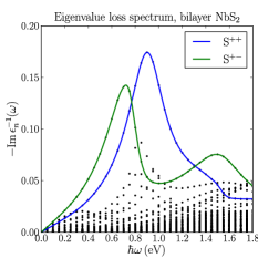
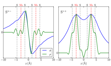
In order to investigate the spatial form of the plasmon modes of the bilayer we follow a recently developed method.Andersen et al. (2012) As explained in Sec. II.1 the full dielectric matrix is diagonalized for each frequency point to obtain its eigenvalues, and left and right eigenfunctions, and . The imaginary part of the inverse eigenvalues, , then provide a resolution the loss spectrum into independent dielectric eigenmodes. Modes corresponding to distinct peaks in the eigenvalue loss spectrum can be identified as the plasmon modes of the system, and the corresponding left and right eigenfunctions represent the potential and charge density of the plasmon excitation, respectively.Andersen et al. (2012)
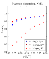
In the left panel of Fig. 4 the eigenvalue loss spectrum is shown for a momentum transfer of Å-1. The soectrum is dominated by two eigenvalue curves, indicated by green and blue solid lines. For comparison, the eigenvalue loss spectrum for the monolayer systems (not shown) reveals a single peak very similar to both the blue curve in Fig. 4 (symmetric mode) and the EELS spectrum of the monolayer (shown in Fig. 1 for TaSe2). Returning to Fig. 4, the eigenvectors belonging to the two peaks reveal an anti-symmetric and symmetric mode, labelled and respectively. The mode corresponds to an out of phase charge oscillation located on the two atoms in the interface. The energy of this mode is significantly red shifted compared to the monolayer plasmon and shows a close to linear dispersion, see right panel of Fig. 4. However, the strength of this mode is vanishing at low , which is possibly related to the close proximity of the two layers. The mode can be characterized as an in-phase oscillation located on the transition metal atoms of the two layers. The induced density () of this mode within each layer is very similar to that found for the plasmon in monolayer NbSe2 (not shown). The mode is blue shifted relative to the single-layer result, particularly in the small regime where the overlap between the potentials from the two layers is largest (recall the potential of a 2D charge density wave decays as )ferrell .
IV Conclusion
In conclusion, we have investigated the plasmonic properties of six monolayers of metallic transition metal dichalchogenides using first-principles calculations. Significant deviations from a 2D free-electron model were found due to coupling to interband transitions which redshift the plasmon energy by up to 1 eV. For momentum transfers of Å-1 the plasmon enters the dissipative electron-hole continuum. For a bilayer NbSe2 structure we found two plasmon modes which can be regarded as symmetric and anti-symmetric combinations of two unperturbed monolayer plasmons. The anti-symmetric mode shows close to linear dispersion, but has very small strength, while the dispersion of the symmetric mode follows the monolayer plasmon with a slight blue shift.
V Acknowledgements
KST acknowledges support from the Danish Council for Independent Research’s Sapere Aude Program through grant no. 11-1051390. The Center for Nanostructured Graphene (CNG) is sponsored by the Danish National Research Foundation, Project DNRF58.
References
- [1]
- Britnell et al. [2012] L. Britnell, R. V. Gorbachev, R. Jalil, B. D. Belle, F. Schedin, A. Mishchenko, T. Georgiou, M. I. Katsnelson, L. Eaves, S. V. Morozov, et al., Science 335, 947 (2012).
- Wang et al. [2012] Q. Wang, K. Kalantar-Zadah, A. Kis, J. Coleman, and M. Strano, Nature Nanotechnology 7, 699 (2012).
- Radisavljedic et al. [2011] B. Radisavljedic, A. Radenovic, J. Brivio, V. Giacometti, and A. Kis, Nature Nanotechnology 6, 147 (2011).
- Splendiani et al. [2010] A. Splendiani, L. Sun, Y. Zhang, T. Li, J. Kim, C.-Y. Chim, G. Galli, and F. Wang, Nano Lett. 10, 1271 (2010).
- Mak et al. [2010] K. F. Mak, C. Lee, J. Hone, J. Shan, and T. F. Heinz, Phys. Rev. Lett. 105, 136805 (2010).
- [7] A. K. Geim and I. V. Grigorieva, Nature 499, 419-425 (2013)
- [8] A. Castellanos-Gomez et al. Nano Research 6, 191 (2013)
- [9] A. Ayari, E. Cobas,O. Ogundadegbe, and M. S. Fuhrer, J. Appl. Phys. 101, 014507 (2007).
- [10] N. E. Staley, J. Wu, P. Eklund, Y. Liu, L. J. Li, and Z. Xu, Phys. Rev. B 80, 184505 (2009).
- Ju et al. [2011] L. Ju, B. Geng, J. Horng, C. Girit, M. Martin, Z. Hao, H. A. Bechtel, X. Liang, A. Zettl, Y. R. Shen, et al., Nature Nanotechnology 6, 630 (2011).
- Chen et al. [2012] J. Chen, M. Badioli, P. Alonso-Gonzalez, S. Thongrattanasiri, F. Huth, J. Osmond, M. Spasenovic, A. Centeno, A. Pesquera, P. Godignon, et al., Nature 487, 77 (2012).
- [13] Y. Liang and S. L. Cundy, Philos. Mag. 19, 1031 (1969).
- König et al. [2012] A. König, K. Koepernik, R. Schuster, R. Kraus, M. Knupfer, B. Büchner, and H. Berger, Europhys. Lett. 100, 27002 (2012).
- Cudazzo et al. [2012] P. Cudazzo, M. Gatti, and A. Rubio, Phys. Rev. B 86, 075121 (2012), URL http://link.aps.org/doi/10.1103/PhysRevB.86.075121.
- Faraggi et al. [2012] M. N. Faraggi, A. Arnau, and V. M. Silkin, Phys. Rev. B 86, 035115 (2012), URL http://link.aps.org/doi/10.1103/PhysRevB.86.035115.
- Prodan et al. [2003] E. Prodan, C. Radloff, N. J. Halas, and P. Nordlander, Science 302, 419 (2003).
- Wang et al. [2007] H. Wang, D. W. Brandl, P. Nordlander, and N. J. Halas, Accounts of Chemical Research 40, 53 (2007), pMID: 17226945, URL http://pubs.acs.org/doi/abs/10.1021/ar0401045.
- [19] X. Zhu, L. Shi, M. S. Schmidt, A. Boisen, O. Hansen, J. Zi, S. Xiao, and N. A. Mortensen, Nano Lett. DOI: 10.1021/nl402120t
- [20] P. Johari and V. B. Shenoy, ACS Nano 5, 5903 (2011).
- [21] J. P. Perdew, K. Burke, and M. Ernzerhof Phys. Rev. Lett. 77, 3865 (1996)
- Enkovaara et al. [2010] J. Enkovaara, C. Rostgaard, J. J. Mortensen, J. Chen, M. Dulak, L. Ferrighi, J. Gavnholt, C. Glinsvad, V. Haikola, H. A. Hansen, et al., Journal of Physics: Condensed Matter 22, 253202 (2010), ISSN 0953-8984.
- [23] O. Gritsenko, R. van Leeuwen, E. van Lenthe, and E. J. Baerends, Phys. Rev. A 51, 1944 (1995).
- Kuisma et al. [2010] M. Kuisma, J. Ojanen, J. Enkovaara, and T. Rantala, Physical Review B 82, 115106 (2010).
- [25] D. Bohm and D. Pines, Phys. Rev. B 92, 602 (1953)
- Yan et al. [2011] J. Yan, J. J. Mortensen, K. W. Jacobsen, and K. S. Thygesen, Physical Review B 83, 245122 (2011), URL http://link.aps.org/doi/10.1103/PhysRevB.83.245122.
- Rozzi et al. [2006] C. A. Rozzi, D. Varsano, A. Marini, E. K. U. Gross, and A. Rubio, Physical Review B 73, 205119 (2006).
- [28] R. A. Ferrell, Phys. Rev. 111, 1214 (1958).
- Andersen et al. [2012] K. Andersen, K. W. Jacobsen, and K. S. Thygesen, Physical Review B 86, 245129 (2012), URL http://link.aps.org/doi/10.1103/PhysRevB.86.245129.
- [30] C. Ataca, H. Sahin, and S. Ciraci, J. Phys. Chem. C 116, 8983 (2012)
- [31] E. H. Hwang, S. Das Sarma, Phys. Rev. B 75, 205418 (2007)
- [32] F. Aryasetiawan and K. Karlsson, Phys. Rev. Lett. 73, 1679 (1994)