Large spin splitting in the conduction band of transition metal dichalcogenide monolayers
Abstract
We study the conduction band spin splitting that arises in transition metal dichalcogenide (TMD) semiconductor monolayers such as MoS2, MoSe2, WS2 and WSe2 due to the combination of spin-orbit coupling and lack of inversion symmetry. Two types of calculation are done. First, density functional theory (DFT) calculations based on plane waves that yield large splittings, between 3 and 30 meV. Second, we derive a tight-binding model, that permits to address the atomic origin of the splitting. The basis set of the model is provided by the maximally localized Wannier orbitals, obtained from the DFT calculation, and formed by 11 atomic-like orbitals corresponding to and orbitals of the transition metal (W,Mo) and chalcogenide (S,Se) atoms respectively. In the resulting Hamiltonian we can independently change the atomic spin-orbit coupling constant of the two atomic species at the unit cell, which permits to analyse their contribution to the spin splitting at the high symmetry points. We find that —in contrast to the valence band— both atoms give comparable contributions to the conduction band splittings. Given that these materials are most often doped, our findings are important for developments in TMD spintronics.
I Introduction
Spin-orbit and exchange are the two dominant spin dependent interactions in solids. Whereas the exchange splitting is only present in magnetic materials, spin-orbit coupling (SOC) is ubiquitous. The proposal of various physical effects driven by spin-orbit interactions, such as the Spin Hall effect, both extrinsicHirsch99 and intrinsic,Murakami03 ; Sinova04 as well as the Quantum Spin Hall phase,Kane-Mele05 ; Bernevig06 together with their experimental confirmation,Valenzuela06 ; Konig07 is opening new venues, enlarging the set of materials that could give rise to practical spintronic devices. The effects of spin-orbit interaction are particularly notorious in materials without inversion symmetry,RMP-Niu because they present spin splitting of the bands and the anomalous velocity is non-zero.
From this perspective, the new generationreview1 ; review2 ; review3 ; Geim13 of semiconducting two dimensional (2D) crystals, such as transition metal dichalgonides (TMD) monolayers (ML), is particularly appealing. The spin-orbit interaction of the constituent atoms is large and those 2D crystals have no inversion symmetry. The resulting spin splitting of the bands gives rise to the so called spin-valley coupling,Xiao which has been experimentally confirmed.review3 ; SV1 ; SV2 ; SV3 ; SV4 ; Zeng2012 This effect is conspicuously apparent in the valence band (VB) of these materials showing the SOC splittings ranging between 150 meV (MoS2) up to to 400 meV (WSe2). The effect of SOC in the conduction band (CB), in contrast, have been overlooked except for a few instances.Kadantseva12 ; Cheiw12 ; Kosmider13 ; Kormanyos13 However, given that very often 2D TMD can be -doped and the conduction band spin splitting is definitely non-zero, it is of the largest interest to study this effect.
The origin of the large spin-orbit splitting of the VB is well understood: at the points, the valence band Bloch states wave are mostly made of the metal orbitals with , where labels the valley index.Zhu12 Therefore, the component of SOC naturally gives a valley dependent splitting of the bands. In contrast, the dominant contribution of the CB lowest energy state comes from the =0 orbitals, that cancels the spin orbit splitting, calculated at first in perturbation theory. Thus, the conduction band spin splitting was neglected in the influential seminal work of Xiao et al. Xiao , proposing a kp model, and most of the papers that followed. Only very recently attention is being payed to the conduction band splitting,Ochoa-Roldan ; Kormanyos13 using an extension of the kp original model,Xiao showing that inter-band coupling to remote bands, results in a finite CB splitting. However, the use of Bloch states inherent in this method obscures the atomic origin of the spin splitting, which remains to be determined and is the main focus of the present work.
In order to address the relative contributions to the CB splitting of the two chemical species in the unit cell it would be convenient to describe the electronic structure of MoS2 and related 2D crystals in terms of localized atomic orbitals. However, most of the existing density functional theory (DFT)KS-PR calculations of the spin-orbit properties of these materials use plane waves as a basis set.Kormanyos13 ; Kosmider13 ; Zhu12 ; Ramasubramaniam11 ; Ramasubramaniam12 ; Britnell ; Wirtz13 In order to bridge the gap between plane wave and atomistic descriptions we make use of the tight-binding (TB) Hamiltonian with a minimal basis set formed by the maximally localized Wannier functions (MLWFs). Marzari This approach keeps a precision of the plane wave calculations,Shi13 ; Espejo13 and at the same time allows a description of the spin-orbit coupling using the intra-atomic terms . Similar approach (we call it TB+SOC) was used to study the Bi2Te3, Bi2Se3, Sb2Te3 topological insulators,Zhang10 and its important advantage is that the atomic SOC of the transition metal (TM) and chalcogenide (CH) atoms, can be varied as the and parameters, which permits to trace the origin of the spin splitting of the different bands. The study of spin orbit coupling physics in other two dimensional crystals, such as graphene, using the atomic Hamiltonian has revealed very fruitful in the past.Min06 ; Huertas06 ; Huertas09 ; Neto09 ; Fabian2010 ; Dani2011 ; Fratini13
The rest of this paper is organized as follows. In section II we present the DFT methodology and the electronic structure of the four two dimensional crystals studied here, MoS2, WS2, MoSe2 and WSe2. In section III we describe the way of obtaining the MLWF basis and the resulting TB Hamiltonian. In section IV we include SOC to the TB Hamiltonian as a sum of atomic terms which depend on the and parameters, and we determine values of these parameters. In section V we take advantage of the model of section IV to discuss the relative contribution to the spin-orbit splitting of the conduction band of the two chemical species of the unit cell. In section VI we discuss the limitations of the model and we present our main conclusions.
II Electronic structure using DFT
We now review the electronic properties of the MoS2, MoSe2, WS2, and WSe2 MLs calculated with DFT in the plane wave basis as implemented in the VASP package.VASP1 We take an energy cutoff =400 eV. We use the projector-augmented waves (PAW)Blochl1 ; Kresse1 method with the , , valence states of the TM atom, and the , valence states of the CH atoms. The Perdew-Burke-Ernzerhof’sPBE version of generalized gradient approximation is used to describe the exchange correlation density functional. We use the super-cell of the 11 periodicity and a vacuum not thinner than 17 Å. The Brillouin Zone (BZ) is sampled with the -centered () Monkhorst-Pack’sMonkhorst mesh of k-points. We carry out two kinds of calculations. One with SOC included and the second one without SOC. From now on we refer to them as to the DFT and DFT+SOC respectively. In the DFT+SOC calculations we use non-collinear versionHoobs of the PAW method and SOC is described using the spherical part of the Kohn-Sham potential inside the PAW spheres.KresseSOC
| (meV) | |||||
| Method | MoS2 | WS2 | MoSe2 | WSe2 | |
| DFT+SOC | C | -3 | 27 | -21 | 38 |
| V | 147 | 433 | 186 | 463 | |
| V1 | 24 | 70 | 27 | 88 | |
| V2 | -50 | -55 | -188 | -232 | |
| TB+SOC | C | -4 | 17 | -28 | -3 |
| V | 147 | 433 | 186 | 463 | |
| V1 | 24 | 66 | 29 | 64 | |
| V2 | -50 | -55 | -188 | -232 | |
| PT | C | -1 | 13 | -11 | 7 |
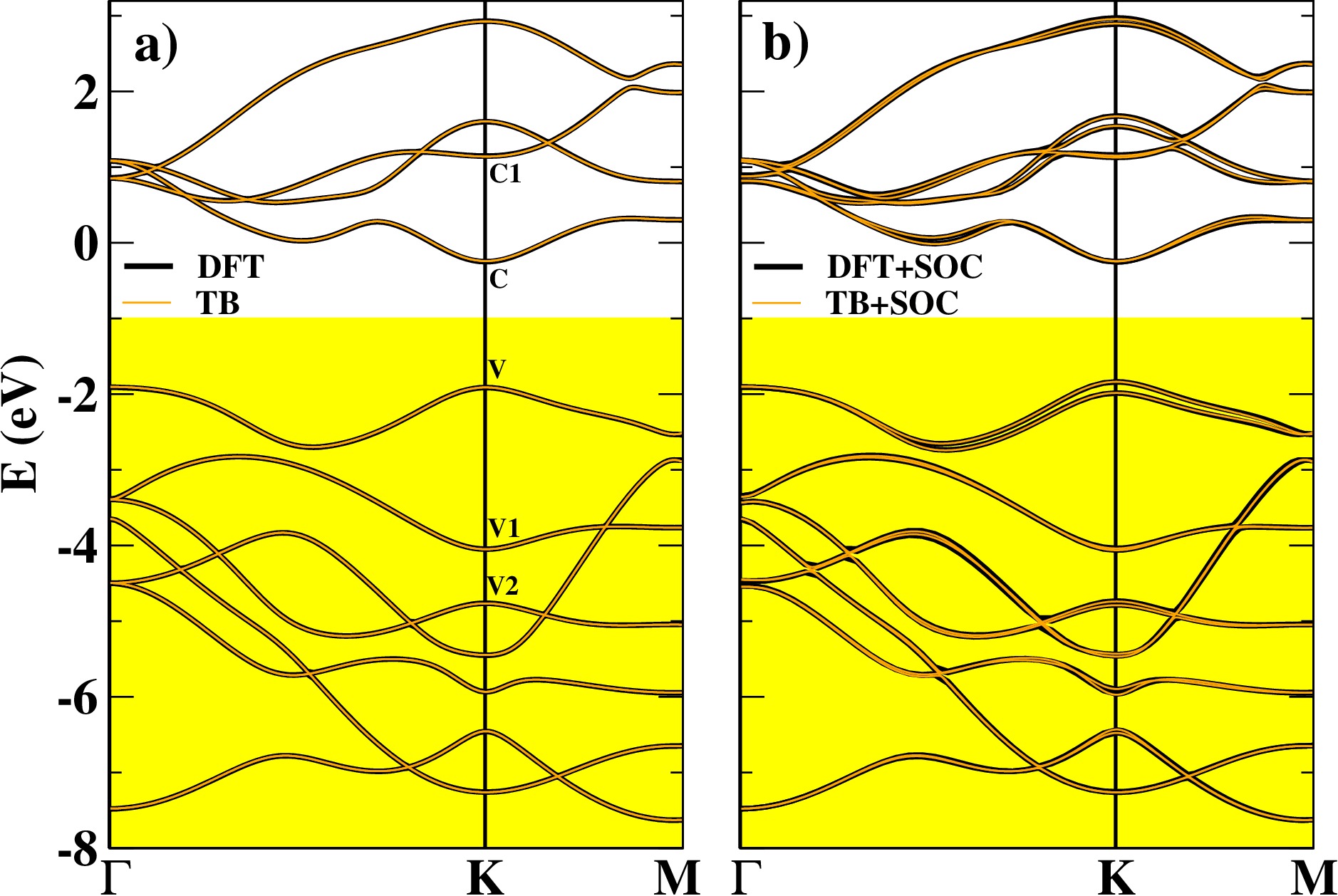
We briefly summarize the main features of the MoS2 ML energy bands, as given by DFT and DFT+SOC (Fig.1(a) and Fig.1(b) respectively). The results for the MoSe2, WS2 and WSe2 MLs are very similar, and agree with the previous calculations.Zhu12 ; Kadantseva12 ; Cheiw12 ; Ramasubramaniam12 ; Kosmider13 The band gap of these semiconducting MLs is direct, with the minimum of the CB and the top of the VB located at the and points of the BZ. All the bands at the points are spin split, but only in some instances the splitting is so large that is appreciated by inspection in Fig.1(b).
Analysis of the wave functions reveals that it is possible to assign a spin projection along the normal to the plane to the different Bloch states in the neighbourhood of the point. Taking advantage of this, in the following we define the splitting of a energy band with momentum k as
| (1) |
With this convention, the splitting can be either positive or negative. Time reversal symmetry warrants that which implies that spin splittings have opposite signs in and valleys.Xiao The spin splittings of the relevant bands at the point are listed in Table 1. The spin-orbit splitting at the top of the VB, range between 147 meV for MoS2 and 463 meV for WSe2. The same splittings for the CB vary from meV for MoS2 to 38 meV for WSe2. They are smaller than those of the VB, but definitely large enough as to be observed. It is worth noticing that only in the case of the conduction band the sign of is not the same for all the compounds, for reasons explained below.
We now discuss the population analysis of the DFT Bloch states. This sheds some light on the origin of their spin splittings. Both VB and CB are predominantly made of the TM atom (=2) orbitals and a smaller but not negligible contribution coming from the (=1, =) orbitals of the chalcogen atoms. The main difference between VB and CB bands lies in the number of orbitals, which is equal in the VB and 0 in the CB. This picture is in agreement with earlier work.Xiao ; Kormanyos13 ; Kosmider13 ; Cheiw12 ; Kadantseva12 ; Zhu12 In the discussion below we shall also make use the fact that the Bloch state labelled as V2 at the point is made exclusively of the chalcogen orbitals (=1, =+1), without mixing to the metal orbitals.
III Maximally localized Wannier functions basis
The Wannier functions Wannier (WF) permit to define a localized basis set by performing a unitary transformation over a set of Bloch states that diagonalize the DFT Hamiltonian. Although there is not a unique way of doing such a , we adopt the method criteria of maximal localizationMarzari and we use the Wannier90WANNIER90 code to find the basis of MLWFs. This approach has already been used for MoS2 and related transition metal dichalcogenides before,Feng_PRB2012 obtaining results in line with those discussed here. In our case, the set is formed by the group of 11 bands distributed around the band gap, as shown in Fig. 1(a).
The first step of the procedure consist of the projection of the the Bloch states over certain a set of localized functions which, in this case, are taken as the and atomic orbitals of the chalcogenide and metallic atom respectively, motivated by the population analysis discussed above. Importantly, in the case of 2D TMDC, the MLWF are centered around the atoms, their localization radius is smaller than the interatomic distance and, in the neighborhood of the atoms, they have the symmetry of the real spherical harmonics. A numerical measure of the localization is given by the localization functionalMarzari . In our case, after 100 iterative steps, we obtain a total spread 18.23/20.85/20.28/23.25 Å2, summing over the 11 Wannier orbitals, for MoS2/MoSe2/WS2/WSe2, which yields an average size per Wannier orbital of 1.29/ 1.38/1.36/1.45 Å.
The isosurfaces of the MLWF obtained for MoS2 are presented in Fig. 2. Their real spherical harmonic symmetry is apparent. In the following we label the MLWF as , where R defines a unit cell inside the crystal and refers to one the 11 atomic-like MLWF inside the unit cell. We refer to them using their real spherical harmonic symmetry, as shown in Fig. 2. However, the shape (not shown) of the tails of the MLWF is different from that of the core. Therefore, MLWFs are not identical to atomic orbitals for which the angular symmetry is independent of the distance to the nuclei.
III.1 Wannier Hamiltonian
The wannierization procedure yields the basis of 11 atomic-like orbitals , and —more importantly— a faithful representation of the DFT Hamiltonian in that basis. Thus, for a given pair of the atomic-like MLWF orbitals and , located in unit cells R and , we obtain the representation of the DFT Hamiltonian . Taking advantage of the Bloch theorem, the Hamiltonian for the entire crystal can be block diagonalized in the usual way, resulting in the following wave-vector dependent Hamiltonian matrix:
| (2) |
where the sum runs over all the unit cells of the crystal, labelled with R. In practice, the localized nature of the MLWFs permits to truncate the sum down to a few neighbors. Importantly, the dimension of the matrix (2) is as small as the size of the MLWF basis (11 in the present case) which makes the numeric diagonalization computationally inexpensive. The resulting energy bands are —not surprisingly (given their formal equivalence)— very similar to those obtained from DFT as shown in Fig. 1(a). Minor differences (not appreciated at the energy scale used in the figure) arise from the truncation in the number of bands, i.e., due to inter band coupling to remote high and low energy bands that have been excluded in the Wannier Hamiltonian but are present in the DFT calculation.
The eigenstates of Hamiltonian (2) are a linear combination of the MLWFs which —as discussed above— have real spherical harmonic symmetry close to the atom cores. In order to understand the spin splittings, it is convenient to define a new basis of orbitals localized around atom , denoted by , which has the symmetry of the eigenstates of the atomic angular momentum operator. In other words, we move from a real basis to the usual spherical harmonics with well defined . In the rest of this paper we use the following notation to relate the Bloch states at the point with the atomically localized orbitals :
| (3) |
where and are coefficients, and ( for the bands C, V, V1 and for C1 and V2).
| MoS2 | WS2 | MoSe2 | WSe2 | |||||||||||
|---|---|---|---|---|---|---|---|---|---|---|---|---|---|---|
| TM | CH | |||||||||||||
| C1 | 0.63 | 0.19 | 0.63 | 0.19 | 0.65 | 0.18 | 0.65 | 0.18 | ||||||
| C | 0 | 0.86 | 0.07 | 0.90 | 0.05 | 0.86 | 0.07 | 0.89 | 0.05 | |||||
| V | 0.80 | 0.10 | 0.79 | 0.11 | 0.82 | 0.09 | 0.79 | 0.10 | ||||||
| V1 | 0.28 | 0.36 | 0.25 | 0.38 | 0.34 | 0.33 | 0.30 | 0.35 | ||||||
| V2 | — | — | 0.5 | — | 0.5 | — | 0.5 | — | 0.5 | |||||
Importantly, since the MLWFs do not rigorously have spherical harmonic symmetry, the are not rigorously eigenstates of the atomic angular momentum operator. However, in the rest of this work, we adopt the approximation that the are indeed eigenstates of the atomic orbital angular momentum operator. The validity of this approach is justified by the fairly good agreement with the DFT results, discussed below.
In Table 2 we show and . It is apparent that the CB and VB are mostly made of the transition metal orbitals, with equal 0 and 2 respectively. The small variations of the coefficient squares and along the different materials inform of their similar electronic structure. It must be noticed that the contributions of the orbitals localized on the CH atoms is larger than 10, and thereby they can account for a fraction of the spin splitting, as it actually happens. Inspection of the wave functions also reveals their odd/even character with respect to reflection across the plane. Specifically, the wave functions of bands C and V are even and those of bands C1, V1, and V2 are odd, in agreement with previous results.Kormanyos13
IV Atomic SOC
The Wannier Hamiltonian just described is derived from a DFT calculation where SOC has been deliberately excluded. We now proceed to add the atomic spin orbit coupling into the TB Hamiltonian
| (4) |
where is a scalar that measure the strength of the atomic SOC, is the angular momentum operator acting on an atom , and are the spin Pauli matrices operators. As discussed after Eq. (3), we assume that
| (5) |
The addition of to Hamiltonian (2) leads to the following TB Hamiltonian
| (6) |
which is the main result of this work. The presence of in Eq. (6) causes spin splittings , which depend on two parameters and .
We are now in position of achieving two goals. First, we can verify the validity of our approach fitting the parameters that give a best agreement between the bands of Hamiltonian (6) and those obtained with the DFT+SOC method, paying special attention to the spin splittings close to the point. Second, we can determine the contribution each atom to the spin-orbit splitting a various bands, with an attention to the conduction band.
IV.1 Perturbative estimate of
It is very instructive to obtain formal expressions for the splittings treating to first order in perturbation theory. A comparison of these expressions with the values calculated using DFT+SOC method yields a first estimate for and . Choosing as the spin quantization axis, the shift of the levels with spin , to first order in perturbation theory, reads:
| (7) |
Since there are two unknowns, we implement this procedure with two bands, and at the point. In the case of V2 the contribution from the TM is strictly null, so that first order perturbation theory yields:
| (8) |
which permits to relate directly the splitting of the V2 band at the point with the chalcogenide spin orbit coupling. In the case of the VB the first order perturbation theory yields:
| (9) |
Combining these two equations, we obtain an estimate for and , shown in the PT columns of Table 3, together with the estimates using a non-perturbative fitting described below.
The first point to notice is that across different materials (except in the case of Se) the values of undergo variations smaller than . This is in line with the general notion that for a given atom, spin-orbit coupling does not vary much from compound to compound. These small variations are a first indication of the validity of our methodology. The second point is that these values are in line with those reported for neutral S/Se atoms (50/220 meV) Wittel as well as for Mo (78 meV ). Dunn Moreover, it must be kept in mind that the localization of Wannier and atomic orbitals can be different. Thereby, a scaling of the for the Wannier orbitals, compared to the atomic orbitals, is expected. Our calculations indicate that this is not a large effect, endorsing the notion that the MLWF used in our calculation are similar to the atomic orbitals.
| (meV) | (meV) | ||||
|---|---|---|---|---|---|
| PT | TB+SOC | PT | TB+SOC | ||
| MoS2 | 87 | 86 | 50 | 52 | |
| WS2 | 274 | 271 | 55 | 57 | |
| MoSe2 | 94 | 89 | 188 | 256 | |
| WSe2 | 261 | 251 | 232 | 439 | |
IV.2 Non perturbative determination of
We now discuss a second and more accurate way to determine the and parameters. For a given value of and , numerical diagonalization of this Hamiltonian yields a set of spin split bands.
As in the perturbative case, we determine ’s by fitting the spin splitting at the point of both valence and V2 bands to those obtained in the DFT+SOC calculations. The values of and parameters estimated this way are listed in the TB+SOC columns of Table 3. They are close to the PT values except the in the WSe2 ML. Possible explanations for this are detailed below.
In Fig. 1 we show a comparison of the DFT+SOC bands (left panel) and with the just described TB+SOC method (right panel). It is notorious that, fixing the splitting of two bands at the point, yields a fairly good agreement for all the bands on the entire Brillouin zone, giving additional support to the methodology.
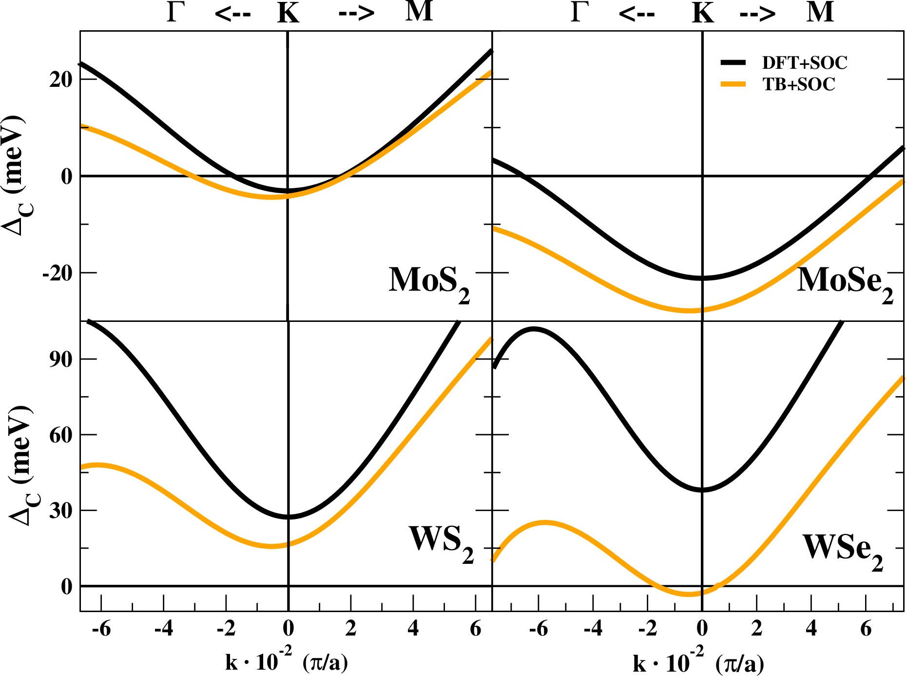
A more quantitative comparison between the TB+SOC and the DFT+SOC calculations is shown in Table 1 where we compare the spin splitting of several bands at the point obtained with the two methods. Of course, by construction of the method, the agreement for the VB and V2 is perfect. In addition, it is apparent that the TB+SOC provides a fairly good quantitative agreement for the spin splitting of the conduction and V1 bands, except for WSe2. In Fig. 3 we compare for DFT+SOC and TB+SOC along the high symmetry points. It is apparent that the TB method captures the non-trivial momentum dependence featured by the DFT+SOC, although there is a systematic off-set which is also larger for WSe2.
V Conduction band spin-orbit splitting
We are now in a position to discuss the mechanism for the conduction band splitting in the TMD monolayers. Inspection of the values in Table 2 reveals, that should vanish to first order in , and have a small linear contribution in . To check this out we plot in Fig. 4 the splitting, keeping one of the values as given in table III (TB+SOC values), and varying the other. The dependence (for ) is a straight line with negative slope. This can be understood within 1st order perturbation theory, that yields the following expression for the chalcogen atom SOC contribution to the splitting:
| (10) | |||||
where the negative sign comes from the fact that, at the point, the CB Bloch state overlaps with the chalcogenide atomic like state (see Table 2). With this equation the negative slopes in Fig. 4(b) became clear. They are controlled by (see Table 2), and are the same for the tungsten based WS2 and WSe2 compounds as well as molybdenum based MoS2 and MoSe2 compounds.

In contrast, the dependence (for ) is not linear —reflecting the inter band character of this contribution— and has a positive sign. Of course, opposite signs and trends are found at the point, on account of time reversal symmetry. The well defined sign of the inter-band contribution to the CB spin splitting is understood as follows. First, we use second order perturbation theory, that yields positive (negative) shifts via inter-band coupling to states below (above) in energy. Second, given the fact that at the point the Bloch states overlap with states with a well defined handedness, together with the angular momentum conservation, result in a spin-selective inter band coupling. Thus, the TM SOC can connect the CB state () with spin only to the states with the opposite values of (1) and spin (), which happen to be available at the band V1, providing a positive contribution of the shift given by
| (11) |
whereas the coupling of the CB to V1 give a null shift of . In contrast, the CB state with spin , can only connect to states with , which happen to be available at the C1 state, giving a negative shift to the level and thereby another positive contribution to the splitting:
| (12) |
We now define and . Combining Eq. (10)-(12) with Eq. (3), using and , with =C1,V1, we can write the following perturbative expression for the CB spin splitting at the valley:
| (13) |
However, since eV and eV, the two terms proportional to are positive. The values of calculated with Eq. (13) for the four TMD MLs are listed in Table 1 (see row PT). It is apparent that the perturbative calculation captures the trend of the non-perturbative results calculation result and provides a qualitative insight of the contribution of each atom to the conduction band splitting.
In summary, the CB splitting has two contributions with opposite signs. For the K valley, the chalcogen SOC gives a negative contribution and the transition metal a positive one. This explains the material dependent sign. Thus, WS2 combines the largest positive with the smallest negative contribution, resulting in a clearly positive splitting. On the opposite side, MoSe2 combines the smaller TM SOC and the largest CH SOC, resulting in the largest negative contribution. In MoS2 the two competing contributions are the smallest (comparing to the other considered MLs) and go a long way to cancel each other: sulphur alone would give meV whereas Mo alone would give meV.
VI Discussion and Conclusions
We now discuss some of the limitations of our model. First, it is apparent that the agreement between the TB+SOC model and the DFT+SOC results is not good in the case WSe2. This is reflected in the discrepancy of the CB spin splitting shown in Table 1 and in the large variations of the value of determined using perturbation theory and the non-peturbative method (see Table 3). This is due in part to the truncation in the number of bands in the TB method. Interband contributions to bands omitted in the TB model contribute to the spin-orbit splitting, and this effect is of course larger for WSe2 for which both ’s are largest.
A second contribution to this discrepancy might arise from the fact that the MLWF are not exactly the same than atomic orbitals. However, the differences are large only in the interstitial region and should weakly affect the spin-orbit physics. In contrast, the loss of atomic symmetry in the interstitial region clearly explains why our attempts, not discussed above, to parametrize the Wannier-TB Hamiltonian with a Slater KosterSlater-Koster parameters have failed. Therefore, the method discussed in this paper needs to be modified in order to map the DFT calculation into a TB model parametrized with a few Slater Koster parameters, in the line of recent work.tight-binding1 ; tight-binding2 ; tight-binding3 A third missing ingredient in the TB+SOC, compared to the DFT+SOC, are interatomic terms, as opposed to the intra-atomic contributions described in Eq. (4).
In summary, DFT calculations show that semiconducting two dimensional transition metal dichalcogenides have spin orbit splittings at the conduction band that —although smaller than those at the valence band— are definitely large enough to be relevant experimentally. NatureComm2013-Delft In order to understand the chemical origin of the splitting, we have derived a tight-binding Hamiltonian (Eq. (6)) using the maximally localized Wannier functions as a basis. Taking advantage of their atomic like character, it is possible to add the atomic spin orbit coupling operators to the tight-binding model, using the atomic as adjustable parameters. We have found that this method describes very well the bands in the energy range from -8 eV to 3 eV around the Fermi level. The tight-binding model permits to determine that both types of atoms, metal and chalcogen, contribute to the conduction band spin splitting with opposite signs. This naturally explains why conduction band spin-orbit splittings of the WS2 and MoSe2 present opposite signs.
Our findings have implications on a wide array of spin related physical phenomena that are being explored in two dimensional transition metal dichalcogenides and their nanostructures,Klinovaja13 including the conduction band Landau Levels,Niu-LL-2013 spin relaxation, Dery-2013 , exciton spin selection rules,Jones-Nat-Nano13 RKKY coupling, RKKY as well as the spin and valley Hall effects. Feng_PRB2012 ; Xiao ; Shan13
VII Acnlowledgements
We acknowledge fruitful discussions with A. Kormányos, J. Jung, A. H. MacDonald, I. Souza, J. L. Martins, E. V. Castro and J. L. Lado. We thankfully acknowledge the computer resources, technical expertise and assistance provided by the Red Española de Supercomputación. JFR acknowledges financial supported by MEC-Spain (FIS2010-21883-C02-01) and Generalitat Valenciana (ACOMP/2010/070), Prometeo. This work has been financially supported in part by FEDER funds. We acknowledge financial support by Marie-Curie-ITN 607904-SPINOGRAPH.
Note Added: Recently, related work has been posted (Kormanys13b, )
References
- (1) J.E. Hirsch, Phys. Rev. Lett. 83, 1834 (1999).
- (2) S. Murakami, N. Nagaoisa, S. C. Zhang, Science 301, 1348 (2003).
- (3) N. Nagaosa, J. Sinova, S. Onoda, A.H. MacDonald, N.P. Ong Rev. Mod. Phys. 82, 1539 (2010).
-
(4)
C.L. Kane and E.J. Mele, Phys. Rev. Lett. 95, 146802 (2005).
C.L. Kane and E.J. Mele, Phys. Rev. Lett. 95 , 226801 (2005). - (5) B. A. Bernevig, T. L. Hughes, S. C: Zhang, Science 314, 1757 (2006).
- (6) S.O. Valenzuela and M. Tinkham, Nature 442, 176 (2006).
- (7) M. Konig, S. Wiedmann, C. Brune, A. Roth, H. Buhmann, L. W. Molenkamp, X. L. Qi, S. C. Zhang Science 318 , 5851 (2007).
- (8) D. Xiao, M.-C. Chang, Q. Niu, Rev. Mod. Phys. 82, 1959 (2010).
- (9) Q.H. Wang, K. Kalantar-Zadeh, A. Kis, J.N. Coleman, and M.S. Strano, Nature Nanotechnology 7, 699 (2012).
- (10) M. Chhowalla, H.S. Shin, G. Eda, L.-J. Li, K.P. Loh, and H. Zhang, Nature Chemistry 5, 263 (2013).
- (11) M. Xu, T. Liang, M. Shi, and H. Chen, Chem. Rev. 113 (2013).
- (12) A.K. Geim, and I.V. Grigorieva, Nature 499, 419 (2013).
- (13) D. Xiao, G.B. Liu, W. Feng, X. Xu, and W. Yao, Phys. Rev. Lett. 108, 196802 (2012).
- (14) T. Cao et al., Nature Communications 3, 887 (2012).
- (15) H. Zeng, J. Dai, W. Yao, D. Xiao, and X. Cui, Nat. Nano. 3, 490 (2012).
- (16) K. F. Mak, K. He, J. Shan, and T. F. Heinz, Nature Nano. 7, 494 (2012).
- (17) G. Sallen, L. Bouet, X. Marie, G. Wang, C. R. Zhu, W. P. Han, Y. Lu, P. H. Tan, T. Amand, B. L. Liu, and B. Urbaszek, Phys. Rev. B 86, 081301(R) (2012).
- (18) H. Zeng et al., Scien. Rep. 3, 1608 (2013).
- (19) A. Kormányos, V. Zólyomi, Neil D. Drummond, P. Rakyta, G. Burkard, Vladimir I. Fal’ko, Phys. Rev. B 88, 045416 (2013).
- (20) K. Kośmider, and J. Fernández-Rossier, Phys. Rev. B 87, 075451 (2013).
- (21) T. Cheiwchanchamnangij and W.R.L. Lambrecht, Phys. Rev. B 85, 205302 (2012).
- (22) E.S. Kadantseva, and P. Hawrylak, Solid State Commun. 152, 909 (2012).
- (23) Z.Y. Zhu, Y.C. Cheng, and U. Schwingenschlögl, Phys. Rev. B 84, 153402 (2011).
- (24) H. Ochoa and R. Roldán Phys. Rev. B 87, 245421 (2013).
- (25) A. Ramasubramaniam, D. Naveh, and E. Towe, Phys. Rev. B 84, 205325 (2011).
- (26) A. Ramasubramaniam, Phys. Rev. B 86, 115409 (2012).
- (27) L. Britnell, R.M. Ribeiro, A. Eckmann, R. Jalil, B.D. Belle, A. Mishchenko, Y.J. Kim, R.V. Gorbachev, T. Georgiou, S.V. Morozov, A.N. Grigorenko, A.K. Geim, C. Casiraghi, A.H. Castro Neto, and K.S. Novoselov, Science 340, 1311 (2013).
- (28) A. Molina-Sánchez, D. Sangalli, K. Hummer, A. Marini, and L. Wirtz Phys. Rev. B 88, 045412 (2013).
- (29) N. Marzari, A.A. Mostofi, J.R. Yates, I. Souza, and D. Vanderbilt, Rev. Mod. Phys. 84, 1419 (2012).
- (30) H. Shi, H. Pan, Y.W. Zhang, and B.I Yakobson, Phys. Rev. B 87, 155304 (2013).
- (31) C. Espejo, T. Rangel, A.H. Romero, X. Gonze, and G.M. Rignanese, Phys. Rev. B 87, 245114 (2013).
- (32) W. Kohn and L.J. Sham, Phys. Rev. 140, A1133 (1965).
- (33) W. Zhang, R. Yu. H.-J. Zhang, X. Dai, Z. Fang, New Journal of Physics 12, 065013 (2010).
- (34) H. Min, J. E. Hill, N. A. Sinitsyn, B. R. Sahu, L. Kleinman, and A. H. MacDonald, Phys. Rev. B 74, 165310 (2006).
- (35) D. Huertas-Hernando, F. Guinea, and A. Brataas, Phys. Rev. B 74, 155426 (2006).
- (36) D. Huertas-Hernando, F. Guinea, A. Brataas, Phys. Rev. Lett. 103, 146801 (2009).
- (37) A. H. Castro Neto, F. Guinea, Phys. Rev. Lett. 103, 026804 (2009).
- (38) S. Konschuh, M. Gmitra, and J. Fabian Phys. Rev. B 82, 245412 (2010).
- (39) D. Gosálbez-Martínez, J. J. Palacios, and J. Fernández-Rossier, Phys. Rev. B 83, 115436 (2011).
- (40) S. Fratini, D. Gosálbez-Martínez, P. Merodio Camara, and J. Fernández-Rossier, Phys. Rev. B 88, 115426 (2013).
- (41) G. Kresse and J. Furthmüller, Phy. Rev. B 54, 11169 (1996).
- (42) P.E. Blöchl, Phys. Rev. B 50, 17953 (1994).
- (43) G. Kresse and D. Joubert, Phys. Rev. B 59, 1758 (1999).
- (44) J.P. Perdew, K. Burke, and M. Ernzerhof, Phys. Rev. Lett. 77, 3865 (1996).
- (45) H.J. Monkhorst and J.D. Pack, Phys. Rev. B 13, 5188 (1976).
- (46) D. Hobbs, G. Kresse and J. Hafner, Phys. Rev. B 62, 11556 (2000).
- (47) Y.-S. Kim, K. Hummer, and G. Kresse, Phys. Rev. B 80 035203 (2009).
- (48) G.H. Wannier, Phys. Rev 52, 191 (1939).
- (49) A. A. Mostofi, J. R. Yates, Y.-S. Lee, I. Souza, D. Vanderbilt and N. Marzari, Comput. Phys. Commun. 178, 685 (2008).
- (50) W. Feng, Y. Yao, W. Zhu, J. Zhou, W. Yao, D. Xiao, Phys. Rev. B 86, 165108 (2012).
- (51) A. Kokalj, Comp. Mater. Sci. 28, 155 (2003).
- (52) K. Wittel and R. Manne, Theoretica Chimica Acta 33, 347 (1974).
- (53) T.M. Dunn, Trans. Faraday Soc. 57, 1441 (1961).
- (54) J. C. Slater and G. F. Koster, Phys. Rev. 94, 1498 (1954).
- (55) E. Cappelluti, R. Roldán, J. A. Silva-Guillen, P. Ordejón, and F. Guinea Phys. Rev. B 88, 075409 (2013).
- (56) Gui-Bin Liu, Wen-Yu Shan, Yugui Yao, Wang Yao, and Di Xiao Phys. Rev. B 88, 085433 (2013)
- (57) H. Rostami, A.G. Moghaddam, and R. Asgari, Phys. Rev. B 88, 085440 (2013).
- (58) G.A. Steele, F. Pei, E.A. Laird, J.M. Jol, H.B. Meerwaldt, and L.P. Kouwenhoven, Nature Communications 4, 1573 (2013).
- (59) J. Klinovaja and Daniel Loss Phys. Rev. B 88, 075404 (2013)
- (60) X. Li, F. Zhang, and Q. Niu, Phys. Rev. Lett. 110, 066803 (2013)
- (61) Y. Song, and H. Dery, Phys. Rev. Lett. 111, 026601 (2013)
- (62) A. M. Jones, H. Yu, N. J. Ghimire, S. Wu, G. Aivazian, J. S. Ross, B. Zhao, J. Yan, D. G. Mandrus, D. Xiao, W. Yao, and X. Xu Nature Nanotechnology 8, 634 (2013)
- (63) F. Parhizgar, H. Rostami, and R. Asgari Phys. Rev. B87, 125401 (2013)
- (64) Wen-Yu Shan, Hai-Zhou Lu, and Di Xiao Phys. Rev. B 88, 125301 (2013)
- (65) A. Kormányos, V. Zólyomi, N. D. Drummond, G. Burkard, arXiv:1310.7720