Optically Controlled Excitonic Transistor
Abstract
Optical control of exciton fluxes is realized for indirect excitons in a crossed-ramp excitonic device. The device demonstrates experimental proof of principle for all-optical excitonic transistors with a high ratio between the excitonic signal at the optical drain and the excitonic signal due to the optical gate. The device also demonstrates experimental proof of principle for all-optical excitonic routers.
Excitonic devices control potential energy landscapes for excitons, exciton fluxes, emission rates, and other characteristics of excitons. Excitonic devices are used both for studies of basic properties of excitons and for development of excitonic signal processing. The potential advantages of excitonic signal processing include compact footprint and high interconnection speed Baldo09 . The development of excitonic devices, where exciton fluxes are controlled, is mainly concentrated on indirect excitons in coupled quantum wells (CQW) Hagn95 ; Gartner06 ; High07 ; High08 ; Grosso09 ; Remeika09 ; High09 ; Vogele09 ; Kuznetsova10 ; Cohen11 ; Winbow11 ; Schinner11 ; Remeika12 ; Leonard12 and exciton-polaritons in microcavities Amo10 ; Gao12 ; Ballarini12 ; Nguyen13 ; Sturn13 .
An indirect exciton is a bound pair of an electron and a hole in spatially separated QW layers (Fig. 1a). The overlap of electron and hole wavefunctions for indirect excitons can be engineered by the structure design and applied voltage so that lifetimes of indirect excitons can exceed those of regular excitons by orders of magnitude. Long lifetimes allow indirect excitons to travel over sufficiently large distances to accommodate devices. Indirect exciton energy can be controlled by voltage: an electric field perpendicular to the QW plane results in the exciton energy shift , where is the built-in dipole moment of indirect excitons ( is close to the distance between the QW centers for a CQW structure) Miller85 . Control of indirect excitons transport by voltage was demonstrated in electrostatically created in-plane potential landscapes in excitonic ramps Hagn95 ; Gartner06 ; Leonard12 , circuit devices High07 ; High08 ; Grosso09 ; Kuznetsova10 , narrow channels Grosso09 ; Vogele09 ; Cohen11 , traps High09 ; Schinner11 , lattices Remeika09 ; Remeika12 , and conveyers Winbow11 .
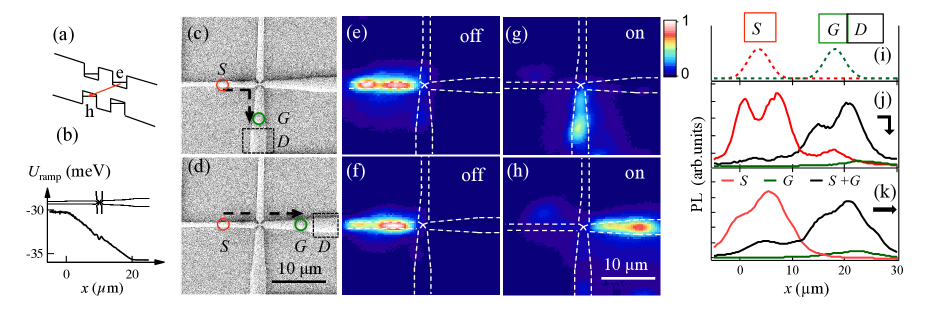
In this work, we study indirect excitons in a crossed-ramp excitonic device. A potential energy gradient - a ramp - is created by a shaped electrode at constant voltage with no energy-dissipating voltage gradient Leonard12 . The design utilizes the ability to control exciton energy by electrode density Kuznetsova10a . An electrode on the sample surface - the top electrode (Fig. 1c,d) - is shaped so that a voltage applied between it and a homogeneous bottom electrode creates two crossing ramps. In each of these ramps, narrowing of the top electrode reduces due to field divergence near the electrode edges and, as a result, increases the exciton energy. The electrode shape (Fig. 1c,d) is designed to obtain a constant potential energy gradient for indirect excitons in the CQW along each of the crossing ramps (Fig. 1b). At the crossing point, the electrodes are narrowed to compensate for the otherwise increased electrode density and thus to keep the exciton energy linear along both ramps Kuznetsova10a . Each of the two ramps is surrounded by flat-energy channels where the electrode width and, in turn, the energy of indirect excitons, is constant (Fig. 1b-d). The parameters of the structure and experimental details are presented in supplementary materials.
The crossed-ramp excitonic device demonstrates experimental proof of principle for all-optical excitonic transistors with optical input, output, and control gate using indirect excitons as the operation medium. Photons transform into excitons at the optical input (source) and travel to the optical output (drain) due to the ramp potential. The output signal of the exciton emission in the drain region is controlled by a gate beam.
Figure 1e,f shows the images of the emission of indirect excitons along the turned-path and straight-path of the crossed-ramp device when only the source beam is on. The corresponding spatial profiles of the indirect exciton emission intensity are presented in Fig. 1j,k. The profile of the source beam is shown in Fig. 1i. The emission patterns show enhanced emission intensity around the excitation spot due to the inner-ring effect studied earlier Ivanov06 ; Hammack09 . The inner ring was explained in terms of exciton transport and cooling: the heating of the exciton gas by laser excitation reduces the occupation of low-energy optically active exciton states, in turn reducing the exciton emission intensity in the excitation spot. When excitons travel away from the excitation spot, they thermalize to the lattice temperature, and the occupation of low-energy optically active exciton states increases, in turn increasing the exciton emission intensity and forming photoluminescence ring around the excitation spot Ivanov06 ; Hammack09 . Emission patterns also show the enhanced emission intensity of indirect excitons at the lower energy side of the ramps due to exciton transport along the potential energy gradient.
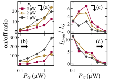
The regime when only the source beam is on refers to off state of the excitonic transistor. The output signal of the transistor given by the emission of indirect excitons in the drain region is weak (Fig. 1j,k). The exciton signal in the drain region is controlled by an optical gate. The positions of the gate beam and drain region are shown in Fig. 1c and Fig. 1d for the turned-path or straight-path operation of the excitonic transistor, respectively. Figure 1j,k shows that turning on the gate beam strongly increases the exciton signal at the drain, switching the excitonic transistor to the on state. Figure 2a,b shows that the on/off ratio of the output intensity in the drain region reaches two orders of magnitude. Furthermore, even a weak gate beam generating a weak exciton signal (green lines in Fig. 1j,k) can strongly increase the output in the drain. Figure 2c,d shows that the ratio between the excitonic signal at the optical drain and the excitonic signal due to the optical gate reaches an order of magnitude. We note that the excitonic signal due to the optical gate is generally smaller than the gate signal since not all of the gate photons transform to the emitted photons due to losses, therefore, in general is not equal to the transistor gain.
The crossed-ramp excitonic device also demonstrates an experimental proof of principle of all-optical excitonic routers. In the absence of the gate beam, the output signal of exciton emission is low in both ramps after the crossing point (Fig. 1e,f). Positioning the gate beam on one or another ramp of the crossed-ramp device determines the path where the output signal is directed (Fig. 1c-h). Even a weak gate beam generating a weak exciton signal can route a much stronger output signal of exciton emission (Fig. 1j,k).
Below we present the theoretical model for the exciton transport in a crossed-ramp device. Indirect exciton transport in a 1D potential energy channel was modeled using the following non-linear transport equation:
| (1) |
This equation was solved for the steady-state distribution of indirect excitons, with (the coordinate follows the path of the exciton flux along the energy channel and ramp). Diffusion and drift fluxes are given by the first and second terms in square brackets, respectively. The exciton diffusion coefficient and mobility are related by the generalized Einstein relationship Ivanov06 ; Hammack09 , where is the quantum degeneracy temperature and is the exciton mass. The drift flux is due to the gradient in the applied ramp potential (shown in Fig. 3d) and the exciton-exciton interaction. The exciton-exciton interaction was modeled as a repulsive dipolar interaction potential, approximated by with , where is the GaAs dielectric constant. The effect of the QW disorder potential is included in the diffusion coefficient, Ivanov06 ; Hammack09 . Here, is the amplitude of the disorder potential and is the diffusion coefficient in the absence of disorder. This description includes (i) increased exciton localization to potential minima for decreasing temperature and (ii) screening of the disorder potential for increasing exciton density Ivanov06 ; Hammack09 .
Optical generation of excitons at the source (gate) is given by . These have Gaussian profiles with position and FWHM chosen to match the experiment. The total injection rate of excitons is where is the width of the potential energy channel. The exciton optical lifetime determines the decay of optically active excitons Ivanov06 ; Hammack09 . The spatially varying exciton temperature used in Eq. (1) is found by solving a thermalization equation:
| (2) |
Here, accounts for energy relaxation of excitons due to bulk longitudinal acoustic phonon emission. is the heating rate due to the non-resonant laser excitation and is determined by the generation rates, and the excess energy of photoexcited excitons . Expressions for , , , and all other parameters of the model are given in Ref. Hammack09 .
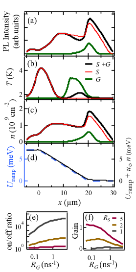
The results of the simulations are presented in Fig. 3. Figure 3d shows the bare ramp potential and the ramp potential screened by the exciton-exciton repulsion . Figures 3a, 3b, and 3c show the emission intensity, temperature, and density of indirect excitons. Figures 3e and 3f show the contrast ratio of the output intensity in the drain region and the gain of the excitonic transistor for different source and gate powers.
Within the model, excitons generated in the gate area screen the disorder in the structure due to the repulsive dipolar interactions of indirect excitons. This increases the source exciton transport distance along the ramp, allowing excitons generated by the source laser to reach the drain region. The transport distance is further enhanced by the gate-beam-induced heating of the exciton gas due to the thermal activation of excitons in the disorder potential. The heating also increases the exciton lifetime that increases the density and, in turn, the screening of the disorder potential. The increasing exciton transport distance along the ramp generates the signal in the drain region. The features observed in the model are qualitatively similar to the experimental data, compare Figs. 1j,k with Fig. 3a, Fig. 2a,b with Fig. 3e, and Fig. 2c,d with Fig. 3f. However, the experimentally observed ratio between the excitonic signal at the optical drain to the excitonic signal due to the optical gate is much higher than the gain of the excitonic transistor calculated within the model. This indicates that a model beyond the considered drift/diffusion model should be developed for a quantitative description of the experimental data.
In summary, we report on experimental proof of principle for all-optical excitonic transistors with a high ratio of the excitonic signal at the optical drain to the excitonic signal due to the optical gate and experimental proof of principle for all-optical excitonic routers.
We thank Marc Baldo, Alexey Kavokin, and Masha Vladimirova for discussions. This work was supported by NSF Grant No. 0907349. P.A. was supported by EU ITN INDEX. S.V.P. was supported by a strategic MIT-Skoltech development program and the Russian Ministry of Education and Science. Y.Y.K. was supported by an Intel fellowship. J.W. was supported by EPSRC. Work in Cardiff University was performed using the computational facilities of the ARCCA Division.
References
- (1) M. Baldo, V. Stojanović, Nature Photonics 3, 558 (2009).
- (2) M. Hagn, A. Zrenner, G. Böhm, G. Weimann, Appl. Phys. Lett. 67, 232 (1995).
- (3) A. Gärtner, A.W. Holleitner, J.P. Kotthaus, D. Schuh, Appl. Phys. Lett. 89, 052108 (2006).
- (4) A.A. High, A.T. Hammack, L.V. Butov, M. Hanson, A.C. Gossard, Opt. Lett. 32, 2466 (2007).
- (5) A.A. High, E.E. Novitskaya, L.V. Butov, A.C. Gossard, Science 321, 229 (2008).
- (6) G. Grosso, J. Graves, A.T. Hammack, A.A. High, L.V. Butov, M. Hanson, A.C. Gossard, Nature Photonics 3, 577 (2009).
- (7) A.A. High, A.K. Thomas, G. Grosso, M. Remeika, A.T. Hammack, A.D. Meyertholen, M.M. Fogler, L.V. Butov, M. Hanson, A.C. Gossard, Phys. Rev. Lett. 103, 087403 (2009).
- (8) X.P. Vögele, D. Schuh, W. Wegscheider, J.P. Kotthaus, A.W. Holleitner, Phys. Rev. Lett. 103, 126402 (2009).
- (9) M. Remeika, J.C. Graves, A.T. Hammack, A.D. Meyertholen, M.M. Fogler, L.V. Butov, M. Hanson, A.C. Gossard, Phys. Rev. Lett. 102, 186803 (2009).
- (10) Y.Y. Kuznetsova, M. Remeika, A.A. High, A.T. Hammack, L.V. Butov, M. Hanson, A.C. Gossard, Opt. Lett. 35, 1587 (2010).
- (11) K. Cohen, R. Rapaport, P.V. Santos, Phys. Rev. Lett. 106, 126402 (2011).
- (12) A.G. Winbow, J.R. Leonard, M. Remeika, Y.Y. Kuznetsova, A.A. High, A.T. Hammack, L.V. Butov, J. Wilkes, A.A. Guenther, A.L. Ivanov, M. Hanson, A.C. Gossard, Phys. Rev. Lett. 106, 196806 (2011).
- (13) G.J. Schinner, E. Schubert, M.P. Stallhofer, J.P. Kotthaus, D. Schuh, A.K. Rai, D. Reuter, A.D. Wieck, A.O. Govorov, Phys. Rev. B 83, 165308 (2011).
- (14) M. Remeika, M.M. Fogler, L.V. Butov, M. Hanson, A.C. Gossard, Appl. Phys. Lett. 100, 061103 (2012).
- (15) J.R. Leonard, M. Remeika, M.K. Chu, Y.Y. Kuznetsova, A.A. High, L.V. Butov, J. Wilkes, M. Hanson, A.C. Gossard, Appl. Phys. Lett. 100, 231106 (2012).
- (16) A. Amo, T.C.H. Liew, C. Adrados, R. Houdré, E. Giacobino, A.V. Kavokin, A. Bramati, Nature Photonics 4, 361 (2010).
- (17) T. Gao, P.S. Eldridge, T.C.H. Liew, S.I. Tsintzos, G. Stavrinidis, G. Deligeorgis, Z. Hatzopoulos, P.G. Savvidis, Phys. Rev. B 85, 235102 (2012).
- (18) D. Ballarini, M. De Giorgi, E. Cancellieri, R. Houdré, E. Giacobino, R. Cingolani1, A. Bramati, G. Gigli, D. Sanvitto, arXiv:1201.4071
- (19) H.S. Nguyen, D. Vishnevsky, C. Sturm, D. Tanese, D. Solnyshkov, E. Galopin, A. Lemaître, I. Sagnes, A. Amo, G. Malpuech, J. Bloch, Phys. Rev. Lett. 110, 236601 (2013).
- (20) C. Sturm, D. Tanese, H.S. Nguyen, H. Flayac, E. Gallopin, A. Lemaître, I. Sagnes, D. Solnyshkov, A. Amo, G. Malpuech, J. Bloch, arXiv:1303.1649
- (21) D.A.B. Miller, D.S. Chemla, T.C. Damen, A.C. Gossard, W. Wiegmann, T.H. Wood, C.A. Burrus, Phys. Rev. B 32, 1043 (1985).
- (22) Y.Y. Kuznetsova, A.A. High, L.V. Butov, Appl. Phys. Lett. 97, 201106 (2010).
- (23) A.L. Ivanov, L.E. Smallwood, A.T. Hammack, Sen Yang, L.V. Butov, A.C. Gossard, Europhys. Lett. 73, 920 (2006).
- (24) A.T. Hammack, L.V. Butov, J. Wilkes, L. Mouchliadis, E.A. Muljarov, A.L. Ivanov, A.C. Gossard, Phys. Rev. B 80, 155331 (2009).