Phase sensitive amplification in silicon photonic crystal waveguides
Yanbing Zhang,1,∗Chad Husko,1Jochen Schröder,1Simon Lefrancois,1
Isabella H. Rey,2 Thomas F. Krauss,2,3 and Benjamin J. Eggleton1
1Centre for Ultrahigh bandwidth Devices for Optical Systems (CUDOS), Institute of Photonics and Optical Science (IPOS),
School of Physics, University of Sydney, NSW 2006, Australia
2SUPA, School of Physics and Astronomy, University of St. Andrews, Fife, KY169SS, UK
3School of Physics, University of York, York, YO10 5DD, UK
∗Corresponding author: y.zhang@physics.usyd.edu.au
Abstract
We experimentally demonstrate phase sensitive amplification (PSA) in a silicon photonic crystal waveguide based on pump-degenerate four-wave mixing. An 11 dB phase extinction ratio is obtained in a record compact 196 nanophotonic device due to broadband slow-light, in spite of the presence of two-photon absorption and free-carriers. Numerical calculations show good agreement with the experimental results.
OCIS codes: 190.4410, 190.4380, 130.5296
Phase sensitive amplification (PSA) is an extremely attractive function for integrated all-optical classical and quantum signal processing due to a wide range of potential applications. In classical communications, PSA is a core technology for noiseless amplification and optical phase regeneration [1, 2, 3, 4], while in quantum processing it is useful for generating squeezed states of light [5, 6] or quantum state translation via Bragg scattering [7, 8]. Despite this progress, the majority of experiments have been in fiber [2, 4] with only a handful of investigations of PSA in centimetre long [9, 10, 3] or devices [11, 12].
Simultaneous to the these developments in large-scale all-optical signal processing, the miniaturization and integration of optical devices onto monolithic photonic chips is rapidly progressing [13, 14]. In order to meet these demanding requirements, the nonlinear elements in current bulk systems must be significantly scaled down in size. To this end, the strong nonlinear response of materials with high refractive index such as semiconductors [13] and chalcogenide glasses [15] enable tight confinement with waveguides centimetres, or even millimetre, scales in lieu of meters of fiber. Silicon is an especially compelling material due to compatibility with CMOS electronics and consequent scope for hybrid opto-electronic chips with unprecedented information processing capabilities [13]. A drawback of the silicon platform in the near-infrared 1.55 m band is the presence of two-photon absorption (TPA) and accompanying free-carriers [16, 17], which limit the desirable Kerr nonlinearity underlying many applications in ultrafast all-optical signal processing.
In this Letter, we demonstrate PSA in a record short 196 m silicon device. By taking advantage of the slow-light enhanced nonlinearity and dispersion engineering capabilities of photonic crystal waveguides (PhCWG) [18, 19], we achieve a phase extinction ratio (PER) of 11 dB in a pump-degenerate four-wave mixing (FWM) scheme. While TPA and free-carrier effects in the silicon material restrict the maximum phase sensitive gain (PSG) [17], we demonstrate that the phase extinction ratio [2], the crucial parameter for phase regeneration, remains essentially unaffected.
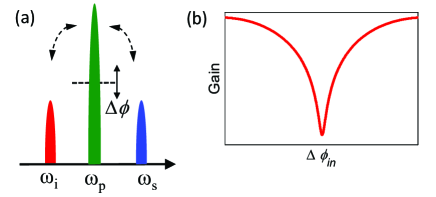
Two common architectures for phase-sensitive amplification using materials are signal-degenerate [2] and pump-degenerate [4] FWM. Fig. 1(a) depicts the principle of phase-sensitive pump-degenerate FWM we employ in our experiments. In this configuration a pump (green) at frequency is converted to an idler (red) and a signal (blue) given by the energy conservation relation . When the pump, signal and idler waves are seeded simultaneously at the input port, the FWM process is phase sensitive with the energy transfer between three waves depending on their relative phase. Therefore, we can control the signal amplification by detuning the phases of the waves, e.g. the pump phase in Fig. 1(b).
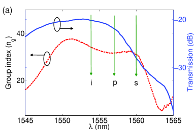
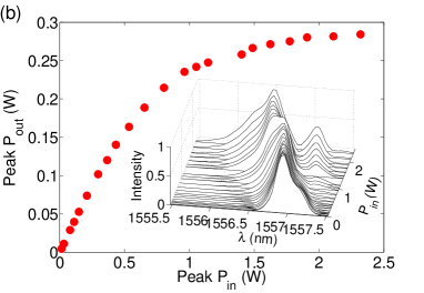
Fig. 1(c) shows the PSA experimental setup. Since the three waves need to be synchronized and phase locked, we generate the signal/pump/idler waves by spectrally slicing the broadband (30 nm) output of a mode-locked Erbium-doped fiber laser (38.6 MHz) using a spectral pulse shaper (SPS1 - Finisar Waveshaper). The resulting idler/pump/signal waves are Gaussian shaped with centre wavelengths at 1554/1557/1560 nm and time durations 8/15.2/8 ps. To avoid FWM inside the EDFA, the signal and idler were delayed by 15/-15 ps with respect to the pump pulse. A second spectral processor (SPS2) is then used to bring the pulses back together and to adjust the peak power and phase of the three waves. The polarization of the light is aligned to the TE slow-light mode of the waveguide by a polarization controller (PC). The input and output powers to the chip were monitored by a power meter (PM) and the output spectra were recorded using an optical spectrum analyzer (OSA).
Figure 2(a) shows the linear transmission (including coupling losses) and group index of the TE mode of the silicon PhCWG. The geometric design of the PhCWG is given in Ref. [20]. The dispersion engineered silicon PhC waveguide has a group index of over a 10 nm bandwidth with negligible dispersion for the pulses considered here (dispersion length cm). Assuming the coupling loss is 9/10dB at the input/output port, the linear propagation loss and the effective nonlinear coefficient were inferred to be around 150 dB/cm at 1557 nm and =4300(W-m)-1 with the slow-down factor [20]. Figure 2(a) also indicates the position of the three waves with pump at 1557 nm exhibiting anomalous dispersion . Note the signal (1560 nm) has a slightly larger propagation loss.
Before the PSA experiments, we first investigated the role of TPA/FCA on the pump propagation. Figure 2(b) shows the measured on-chip output peak power versus coupled input peak power. At large input power, the output power saturates due to strong TPA with the optically generated free-carriers inducing absorption (FCA) further limiting the peak power. The inset shows the corresponding normalized output spectra of the pump as a function of the input peak power. While the TPA attenuates the pulses symmetrically, the time delayed free-carriers affect the trailing edge of the pulse, leading to the asymmetric blue-shift in the pump spectra due to free-carrier dispersion (FCD) [21, 22]. With this knowledge we set the on-chip pump peak power in our first experiment to W to avoid large losses to TPA and FCA. We inject the signal and idler waves with much smaller peak power levels of 40 mW and 10 mW, respectively, well below the nonlinear threshold.
In order to characterize the PSA, we measured the on-chip signal/idler gain by varying the pump phase () while keeping the phases of the signal/idler waves constant at SPS2. Figure 3(a) shows an overlay of output spectra measured at different pump phase shifts of , , and , as well as the unamplified signal/idler waves with no pump. We observe a clear variation in the signal and idler intensities for different values of the pump phase indicating the PSA process is performing as expected. We note the signal intensity is lower than the idler due to the higher propagation loss at the signal wavelength (see Fig. 2(a)) even though we inject a higher power.
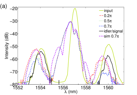
The spectra of Fig. 3(a) also highlight several features of PSA in silicon. In contrast to earlier work in glass materials [1, 12], our demonstration in the semiconductor silicon material includes TPA and free-carriers modulating the PSA process. In particular, free carriers generated by the strong pump, blue-shift the spectra of all three waves (dotted lines), readily seen when comparing the output to the input spectra. While the blue-shift in semiconductors is known from other nonlinear semiconductor experiments [21, 20, 22], this is the first investigation into the role of TPA and free-carriers on the PSA process.
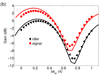
Fig. 3(b) summarizes the experimental signal and idler gain as a function of relative phase detuning over one period. Note that the period of the PSA curve is , due to the factor of two in the FWM phase matching relation for the phase of the pump. We define the on-chip gain as: , the ratio of the amplified signal power with the pump wave switched on over the unamplified signal power without the pump at the output of the waveguide. We employ this definition for simple comparison at the output OSA. We integrate over the signal and idler spectral width to account for self and cross-phase modulation broadening shown in Fig. 3(a). Experimentally, a maximum signal (idler) gain of 0 (2.7) dB is obtained at 0.68 (0.75) and a minimum gain of -10 (-6.8) dB occurs at 0.18 (0.25), yielding an extinction ratio of 10 dB (9.5 dB) for the signal/idler at this power level. We believe the maximum and minimum gain curves are asymmetric due to TPA/FCA limiting the maximum gain, and attribute the difference in gain to the different transmission properties at these wavelengths. Similarly the small phase offset between the signal and idler gain can be explained by free-carriers inducing slightly different FCD (blue shift).
In Fig. 3, we confirm these measurements by numerical solution of the nonlinear Schrödinger equation (NLSE) with split-step Fourier method (SSFM) including up to the 4th order dispersion, TPA and free carriers [16]. The parameters used in the simulation of the PSA experiment are given in Table 1. Note that our model uses slightly different values for the TPA coefficient () and free carrier dispersion () compared to references to most accurately model our experimental results. Here, the linear propagation loss is derived directly from the measured transmission spectrum in Fig. 2(a). The used pump pulse is measured from frequency resolved optical gating (FROG) and the signal/idler are assumed as Gaussian pulses. A free carrier lifetime () is set as 300 ps [21]. The estimated nonlinear effect in the 60 -length input and output nanowire is also negligible compared to the PhC waveguide. The simulation results show good agreement with the experimental observation. Note that the absolute phase in experiment and simulation is ambiguous. Therefore the phase origin of the simulated gain curves were shifted to match the experiments.
| 1.5 W | 42/10.4 mW | ||
| FWHM=15.2 ps | FWHM=5/6 ps | ||
| s4/m | LPhC | 196 m | |
| m2 | m3 | ||
| 300 ps |
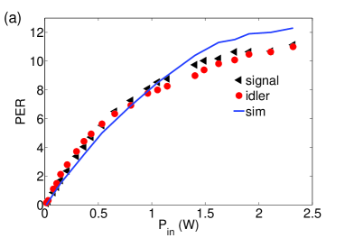
To further explore the dynamics of the PSA process in the presence of TPA and free carriers, we repeated the experiment in Fig. 3 for various input pump powers. Figure 4(a) presents the results of these measurements and unveils additional aspects unique to PSA in silicon in addition to the aforementioned blue-shifted spectra. First, we achieved a maximum extinction ratio of 11 dB (11.5 dB) for the signal (idler) at a pump power of 2.3 W. Importantly the extinction ratios of both the signal and idler are consistent throughout the entire range of power detuning as shown in Fig. 4(a). Based on previous demonstration, this PER is sufficient for phase regeneration [2]. Second, the increase of the extinction ratio slows down at 1.0 W due to the saturating nature of the nonlinearity as indicated earlier in the curve of Fig. 2(b).
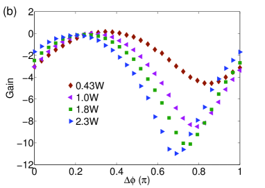
Figure 4(b) shows the phase sensitive gain of the signal wave at four different pump powers from Fig. 4(a). One observes a clear shift of the phase position of the maxima/minima as a function of input power. The underlying physical reasoning is a larger pump power causing a larger nonlinear phase shift () adjusting the phase matching condition. The maximum gain occurs at , where is the relative phase among the three waves with the linear phase from dispersion . Again, the numerical calculation show good agreement with the experimental data.
In summary, we experimentally demonstrated PSA based on pump-degenerate FWM in a record short 196 m photonic chip, in spite the restriction of the maximum gain by TPA. We emphasize these are only first results and several aspects can be further optimised including: shorter pulse duration to reduce free carriers and improve the NL phase shift, improving the linear transmission, and operation closer to the zero dispersion point. We achieved an extinction ratio of 11.5 dB for both the signal and idler beams despite TPA and associated free-carriers without having to resort to P-I-N junctions, demonstrating useful levels of on-chip PSA for all-optical classic and quantum processing.
This work was supported by the Australian Research Councils, Laureate Fellowship (FL120100029),Center of Excellence CUDOS (CE110001018) and Discovery Early Career Researcher (DE120101329, DE120102069) schemes. The authors thank Andrea Blanco-Redondo for discussion in simulation.
References
- [1] C. McKinstrie and S. Radic, Opt. Express 12, 4973 (2004).
- [2] R. Slavík, F. Parmigiani, J. Kakande, C. Lundström, M. Sjödin, P. A. Andrekson, R. Weerasuriya, S. Sygletos, A. D. Ellis, L. Grüner-Nielsen, D. Jakobsen, S. Herstrøm, R. Phelan, J. O’Gorman, A. Bogris, D. Syvridis, S. Dasgupta, P. Petropoulos, and D. J.Richardson, Nat. Photon. 4, 690 (2010).
- [3] T. Umeki, M. Asobe, and H. Takenouchi, Opt. express 21, 12077 (2013).
- [4] Z. Tong, C. Lundström, P. Andrekson, C. McKinstrie, M. Karlsson, D. Blessing, E. Tipsuwannakul, B. Puttnam, H. Toda, and L. Grüner-Nielsen, Nat. Photon. 5, 430 (2011).
- [5] D. Levandovsky, M. Vasilyev, and P. Kumar, Opt. Lett. 24, 984 (1999).
- [6] C. M. Caves, Phys. Rev.D 26, 1817 (1982).
- [7] H. J. McGuinness, M. G. Raymer, C. J. McKinstrie, and S. Radic, Phys. Rev. Lett. 105, 093604 (2010).
- [8] A. S. Clark, S. Shahnia, M. J. Collins, C. Xiong, and B. J. Eggleton, Opt. Lett. 38, 947 (2013).
- [9] K.-J. Lee, F. Parmigiani, S. Liu, J. Kakande, P. Petropoulos, K. Gallo, and D. J. Richardson, Opt. Express 17, 20393 (2009).
- [10] B. J. Puttnam, D. Mazroa, S. Shinada, and N. Wada, Opt. Express 19, B131 (2011).
- [11] N. Kang, A. Fadil, M. Pu, H. Ji, H. Hu, E. Palushani, D. Vukovic, J. Seoane, H. Ou, K. Rottwitt, and C. Peucheret, CLEO: Science and Innovations, OSA, (2013).
- [12] R. Neo, J. Schröder, Y. Paquot, D.-Y. Choi, S. Madden, B. Luther-Davies, and B. J. Eggleton, Opt. Express 21, 7926 (2013).
- [13] J. Leuthold, C. Koos, and W. Freude, Nat. Photon. 4, 535 (2010).
- [14] A. Politi, J. Matthews, M. G. Thompson, and J. L. O’Brien, IEEE J. Sel. Top. in Quantum Electron. 15, 1673 (2009).
- [15] B. J. Eggleton, B. Luther-Davies, and K. Richardson, Nat. Photon. 5, 141 (2011).
- [16] L. Yin and G. P. Agrawal, Opt. Lett. 32, 2031(2007).
- [17] M. A. Foster, A. C. Turner, J. E. Sharping, B. S. Schmidt, M. Lipson, and A. L. Gaeta, Nature 441, 960 (2006).
- [18] J. Li, T. P. White, L. O’Faolain, A. Gomez-Iglesias, and T. F. Krauss, Opt. Express 16, 6227 (2008).
- [19] C. Monat, B. Corcoran, D. Pudo, M. Ebnali-Heidari, C. Grillet, M. D. Pelusi, D. J. Moss, B. J. Eggleton, T. P. White, L. O’Faolain, T. F. Krauss, IEEE J. Sel. Top. in Quantum Electron. 16, 344 (2010).
- [20] J. Li, L. O’Faolain, I. H. Rey, and T. F. Krauss, Opt. Express (2011).
- [21] C. Monat, B. Corcoran, M. Ebnali-Heidari, C. Grillet, B. J. Eggleton, T. P. White, L. O’Faolain, and T. F. Krauss, Opt. Express 17, 2944 (2009).
- [22] C. A. Husko, S. Combrié, P. Colman, J. Zheng, A. De Rossi, and C. W. Wong, Scientific Reports 3 (2013).
References
- [1] C. McKinstrie and S. Radic, “Phase-sensitive amplification in a fiber,” Opt. Express 12, 4973 (2004).
- [2] R. Slavík, F. Parmigiani, J. Kakande, C. Lundström, M. Sjödin, P. A. Andrekson, R. Weerasuriya, S. Sygletos, A. D. Ellis, L. Grüner-Nielsen, D. Jakobsen, S. Herstrøm, R. Phelan, J. O’Gorman, A. Bogris, D. Syvridis, S. Dasgupta, P. Petropoulos, and D. J.Richardson, “All-optical phase and amplitude regenerator for next-generation telecommunications systems,” Nat. Photon. 4, 690 (2010).
- [3] T. Umeki, M. Asobe, and H. Takenouchi, “In-line phase sensitive amplifier based on ppln waveguides,” Opt. express 21, 12077 (2013).
- [4] Z. Tong, C. Lundström, P. Andrekson, C. McKinstrie, M. Karlsson, D. Blessing, E. Tipsuwannakul, B. Puttnam, H. Toda, and L. Grüner-Nielsen, “Towards ultrasensitive optical links enabled by low-noise phase-sensitive amplifiers,” Nat. Photon. 5, 430 (2011).
- [5] D. Levandovsky, M. Vasilyev, and P. Kumar, “Amplitude squeezing of light by means of a phase-sensitive fiber parametric amplifier,” Opt. Lett. 24, 984 (1999).
- [6] C. M. Caves, “Quantum limits on noise in linear amplifiers,” Phys. Rev.D 26, 1817 (1982).
- [7] H. J. McGuinness, M. G. Raymer, C. J. McKinstrie, and S. Radic, enquoteQuantum frequency translation of single-photon states in a photonic crystal fiber, Phys. Rev. Lett. 105, 093604 (2010).
- [8] A. S. Clark, S. Shahnia, M. J. Collins, C. Xiong, and B. J. Eggleton, “High-efficiency frequency conversion in the single-photon regime,” Opt. Lett. 38, 947 (2013).
- [9] K.-J. Lee, F. Parmigiani, S. Liu, J. Kakande, P. Petropoulos, K. Gallo, and D. J. Richardson, “Phase sensitive amplification based on quadratic cascading in a periodically poled lithium niobate waveguide,” Opt. Express 17, 20393 (2009).
- [10] B. J. Puttnam, D. Mazroa, S. Shinada, and N. Wada, “Phase-squeezing properties of non-degenerate PSAs using PPLN waveguides,” Opt. Express 19, B131 (2011).
- [11] N. Kang, A. Fadil, M. Pu, H. Ji, H. Hu, E. Palushani, D. Vukovic, J. Seoane, H. Ou, K. Rottwitt, and C. Peucheret, “Experimental demonstration of phase sensitive parametric processes in a nano-engineered silicon waveguide,” in “CLEO: Science and Innovations,” CLEO: Science and Innovations, OSA, (2013).
- [12] R. Neo, J. Schröder, Y. Paquot, D.-Y. Choi, S. Madden, B. Luther-Davies, and B. J. Eggleton, “Phase-sensitive amplification of light in a photonic chip using a dispersion engineered chalcogenide ridge waveguide,” Opt. Express 21, 7926 (2013).
- [13] J. Leuthold, C. Koos, and W. Freude, “Nonlinear silicon photonics,” Nat. Photon. 4, 535 (2010).
- [14] A. Politi, J. Matthews, M. G. Thompson, and J. L. O’Brien, “Integrated quantum photonics,” IEEE J. Sel. Top. in Quantum Electron. 15, 1673 (2009).
- [15] B. J. Eggleton, B. Luther-Davies, and K. Richardson, “Chalcogenide photonics,” Nat. Photon. 5, 141 (2011).
- [16] L. Yin and G. P. Agrawal, “Impact of two-photon absorption on self-phase modulation in silicon waveguides,” Opt. Lett. 32, 2031(2007).
- [17] M. A. Foster, A. C. Turner, J. E. Sharping, B. S. Schmidt, M. Lipson, and A. L. Gaeta, “Broad-band optical parametric gain on a silicon photonic chip,” Nature 441, 960 (2006).
- [18] J. Li, T. P. White, L. O’Faolain, A. Gomez-Iglesias, and T. F. Krauss, “Systematic design of flat band slow light in photonic crystal waveguides,” Opt. Express 16, 6227 (2008).
- [19] C. Monat, B. Corcoran, D. Pudo, M. Ebnali-Heidari, C. Grillet, M. D. Pelusi, D. J. Moss, B. J. Eggleton, T. P. White, L. O’Faolain, T. F. Krauss, “Slow light enhanced nonlinear optics in silicon photonic crystal waveguides,” IEEE J. Sel. Top. in Quantum Electron. 16, 344 (2010).
- [20] J. Li, L. O’Faolain, I. H. Rey, and T. F. Krauss, “Four-wave mixing in photonic crystal waveguides: slow light enhancement and limitations,” Opt. Express (2011).
- [21] C. Monat, B. Corcoran, M. Ebnali-Heidari, C. Grillet, B. J. Eggleton, T. P. White, L. O’Faolain, and T. F. Krauss, “Slow light enhancement of nonlinear effects in silicon engineered photonic crystal waveguides,” Opt. Express 17, 2944 (2009).
- [22] C. A. Husko, S. Combrié, P. Colman, J. Zheng, A. De Rossi, and C. W. Wong, “Soliton dynamics in the multiphoton plasma regime,” Scientific Reports 3 (2013).