Unified Subharmonic Oscillation Conditions for Peak or Average Current Mode Control

Chung-Chieh Fang
arXiv:1310.7433v1: Oct. 28, 2013; arXiv:1310.7433v2: March 19, 2024.The author is with Sunplus Technology, Hsinchu 300, Taiwan (email: fangcc3@yahoo.com).
Abstract

This paper is an extension of the author’s recent research in which only buck converters were analyzed. Similar analysis can be equally applied to other types of converters. In this paper, a unified model is proposed for buck, boost, and buck-boost converters under peak or average current mode control to predict the occurrence of subharmonic oscillation. Based on the unified model, the associated stability conditions are derived in closed forms. The same stability condition can be applied to buck, boost, and buck-boost converters. Based on the closed-form conditions, the effects of various converter parameters including the compensator poles and zeros on the stability can be clearly seen, and these parameters can be consolidated into a few ones. High-order compensators such as type-II and PI compensators are considered. Some new plots are also proposed for design purpose to avoid the instability. The instability is found to be associated with large crossover frequency. A conservative stability condition, agreed with the past research, is derived. The effect of the voltage loop ripple on the instability is also analyzed.

Index Terms:
current mode control, dc-dc power conversion, stability condition, subharmonic oscillation

I Nomenclature

  • D𝐷D

    duty cycle (Note: dimensionless parameters are highlighted in red)

  • T𝑇T

    switching period

  • fs=1/Tsubscript𝑓𝑠1𝑇f_{s}=1/T

    switching frequency (unit: Hertz)

  • ωs=2πfssubscript𝜔𝑠2𝜋subscript𝑓𝑠\omega_{s}=2\pi f_{s}

    angular switching frequency (unit: rad/s)

  • ωcsubscript𝜔𝑐\omega_{c}

    crossover frequency

  • vssubscript𝑣𝑠v_{s}

    source (input) voltage

  • vosubscript𝑣𝑜v_{o}

    output voltage

  • vrsubscript𝑣𝑟v_{r}

    reference voltage

  • vcsubscript𝑣𝑐v_{c}

    control voltage (at the output of the voltage-loop compensator)

  • vdsubscript𝑣𝑑v_{d}

    voltage across the diode

  • iLsubscript𝑖𝐿i_{L}

    inductor current, a triangular wave in the time domain

  • vL=L(diL/dt)subscript𝑣𝐿𝐿𝑑subscript𝑖𝐿𝑑𝑡v_{L}=L(di_{L}/dt)

    voltage across the inductor, a square wave in the time domain

  • m1subscript𝑚1m_{1}

    inductor current slope diL/dt𝑑subscript𝑖𝐿𝑑𝑡di_{L}/dt when the switch is on

  • -m2subscript𝑚2m_{2}

    (negative) inductor current slope diL/dt𝑑subscript𝑖𝐿𝑑𝑡di_{L}/dt when the switch is off

  • va=vhvlsubscript𝑣asubscript𝑣subscript𝑣𝑙v_{\mathrm{a}}=v_{h}-v_{l}

    amplitude of vLsubscript𝑣𝐿v_{L} (also note: va=L(m1+m2)subscript𝑣a𝐿subscript𝑚1subscript𝑚2v_{\mathrm{a}}=L(m_{1}+m_{2}))

  • vh=Lm1subscript𝑣𝐿subscript𝑚1v_{h}=Lm_{1}

    the high value of vLsubscript𝑣𝐿v_{L}

  • vl=Lm2subscript𝑣𝑙𝐿subscript𝑚2v_{l}=-Lm_{2}

    the low value of vLsubscript𝑣𝐿v_{L}

  • y(t)𝑦𝑡y(t)

    feedback signal for switching (the switch is turned off when yh𝑦y\leq h, for example)

  • h(t)𝑡h(t)

    PWM or stabilizing ramp signal

  • Vhsubscript𝑉V_{h}

    the high value of the ramp

  • Vlsubscript𝑉𝑙V_{l}

    the low value of the ramp

  • Vm=VhVlsubscript𝑉𝑚subscript𝑉subscript𝑉𝑙V_{m}=V_{h}-V_{l}

    ramp amplitude

  • ma=Vm/T=Vmfssubscript𝑚𝑎subscript𝑉𝑚𝑇subscript𝑉𝑚subscript𝑓𝑠m_{a}=V_{m}/T=V_{m}f_{s}

    ramp slope

  • mvsubscript𝑚𝑣m_{v}

    the effect on the required ramp slope masubscript𝑚𝑎m_{a} due to the (added) voltage loop ripple

  • L𝐿L

    inductance

  • C𝐶C

    capacitance

  • C3subscript𝐶3C_{3}

    capacitance of a (ceramic) capicitor (with small ESR) in parallel with C𝐶C

  • R𝑅R

    load resistance

  • Rssubscript𝑅𝑠R_{s}

    sensing resistance (for the inductor current iLsubscript𝑖𝐿i_{L})

  • Rcsubscript𝑅𝑐R_{c}

    equivalent series resistance (ESR) of C𝐶C

  • ρ=R/(R+Rc)𝜌𝑅𝑅subscript𝑅𝑐\rho=R/(R+R_{c})

    a dimensionless parameter to show the effect of Rcsubscript𝑅𝑐R_{c} (ρ=1𝜌1\rho=1 if Rc=0subscript𝑅𝑐0R_{c}=0)

  • ϵ=δTitalic-ϵ𝛿𝑇\epsilon={\color[rgb]{0,0,0}{\delta}}T

    switching delay

  • 𝒯(s)=𝒯i(s)+𝒯v(s)𝒯𝑠subscript𝒯𝑖𝑠subscript𝒯𝑣𝑠\mathcal{T}(s)=\mathcal{T}_{i}(s)+\mathcal{T}_{v}(s)

    loop gain (with two parts contributed by the current and voltage loops)

  • 𝒯(s)=esϵ𝒯(s)superscript𝒯𝑠superscript𝑒𝑠italic-ϵ𝒯𝑠\mathcal{T}^{\prime}(s)=e^{-s\epsilon}\mathcal{T}(s)

    loop gain with a switching delay ϵ:=δTassignitalic-ϵ𝛿𝑇\epsilon:=\delta T

  • 𝒯i(s)subscript𝒯𝑖𝑠\mathcal{T}_{i}(s)

    the part of loop gain contributed by the current loop

  • 𝒯v(s)subscript𝒯𝑣𝑠\mathcal{T}_{v}(s)

    the part of loop gain contributed by the feedback voltage loop

  • 𝒞1subscript𝒞1\mathcal{C}_{1}, 𝒞2subscript𝒞2\mathcal{C}_{2}, 𝒞3subscript𝒞3\mathcal{C}_{3}, etc.

    a case for a typical loop gain (see Table I or [4] for the case number)

  • Kcsubscript𝐾𝑐K_{c}

    compensator gain

  • ωpsubscript𝜔𝑝\omega_{p}

    compensator pole

  • ωzsubscript𝜔𝑧\omega_{z}

    compensator zero

  • ωr=1/RcCsubscript𝜔𝑟1subscript𝑅𝑐𝐶\omega_{r}=1/R_{c}C

    ESR zero

  • ωq=ωr(1+C/C3)subscript𝜔𝑞subscript𝜔𝑟1𝐶subscript𝐶3\omega_{q}=\omega_{r}(1+C/C_{3})

    a pole contributed by adding C3subscript𝐶3C_{3} in parallel with C𝐶C

  • p=ωp/ωs𝑝subscript𝜔𝑝subscript𝜔𝑠p=\omega_{p}/\omega_{s}

    normalized (by ωssubscript𝜔𝑠\omega_{s}) compensator pole

  • z=ωz/ωs𝑧subscript𝜔𝑧subscript𝜔𝑠z=\omega_{z}/\omega_{s}

    normalized compensator zero

  • r=ωr/ωs𝑟subscript𝜔𝑟subscript𝜔𝑠r=\omega_{r}/\omega_{s}

    normalized ESR zero

  • q=ωq/ωs𝑞subscript𝜔𝑞subscript𝜔𝑠q=\omega_{q}/\omega_{s}

    normalized ωqsubscript𝜔𝑞\omega_{q}

  • Gi(s)=Rs/sLsubscript𝐺𝑖𝑠subscript𝑅𝑠𝑠𝐿G_{i}(s)=R_{s}/sL

    current-loop integrator to convert vLsubscript𝑣𝐿v_{L} to RsiLsubscript𝑅𝑠subscript𝑖𝐿R_{s}i_{L} (for modeling purpose only)

  • Gc(s)subscript𝐺𝑐𝑠G_{c}(s)

    current-loop compensator transfer function

  • Gv(s)subscript𝐺𝑣𝑠G_{v}(s)

    voltage-loop compensator transfer function

  • K=vaRsKcVmωzLωs𝐾subscript𝑣asubscript𝑅𝑠subscript𝐾𝑐subscript𝑉𝑚subscript𝜔𝑧𝐿subscript𝜔𝑠K=\frac{v_{\mathrm{a}}R_{s}K_{c}}{V_{m}\omega_{z}L\omega_{s}}

    gain of the current feedback loop for the type-II compensator case

  • K=KzK𝐾𝑧\mathrm{K}=Kz

    gain of the current feedback loop for the PI compensator case

  • Kmaxsubscript𝐾maxK_{\mathrm{max}}

    maximum allowable K𝐾K to avoid subharmonic oscillation (i.e., need K<Kmax𝐾subscript𝐾maxK<K_{\mathrm{max}})

  • KmaxsubscriptKmax\mathrm{K}_{\mathrm{max}}

    maximum allowable KK\mathrm{K} to avoid subharmonic oscillation (i.e., need K<KmaxKsubscriptKmax\mathrm{K}<\mathrm{K}_{\mathrm{max}})

  • Kv=ρvsKcTLCωzsubscript𝐾𝑣𝜌subscript𝑣𝑠subscript𝐾𝑐𝑇𝐿𝐶subscript𝜔𝑧K_{v}=\frac{\rho v_{s}K_{c}}{TLC\omega_{z}}

    gain of the voltage feedback loop for the type-II compensator case

  • k=ρKcT/RsCωz𝑘𝜌subscript𝐾𝑐𝑇subscript𝑅𝑠𝐶subscript𝜔𝑧k=\rho K_{c}T/R_{s}C\omega_{z}

    a dimensionless voltage feedback gain (k=0𝑘0k=0 if the voltage feedback loop is open)

  • α(D,p)𝛼𝐷𝑝\alpha(D,p)

    a function used as a building block of most typical stability conditions

  • αk(D)subscript𝛼𝑘𝐷\alpha_{k}(D)

    the k𝑘k-th coefficient term of α(D,p)=k=0(1)kαk(D)pk𝛼𝐷𝑝superscriptsubscript𝑘0superscript1𝑘subscript𝛼𝑘𝐷superscript𝑝𝑘\alpha(D,p)=\sum\limits_{k=0}^{\infty}(-1)^{k}\alpha_{k}(D)p^{k}

  • c(D,p)𝑐𝐷𝑝c(D,p)

    the high order k2𝑘2k\geq 2 (correction) terms of α(D,p)𝛼𝐷𝑝\alpha(D,p), i.e., c(D,p)=k=2(1)kαk(D)pk𝑐𝐷𝑝superscriptsubscript𝑘2superscript1𝑘subscript𝛼𝑘𝐷superscript𝑝𝑘c(D,p)=\sum\limits_{k=2}^{\infty}(-1)^{k}\alpha_{k}(D)p^{k}

  • kpsubscript𝑘𝑝k_{p}

    proportional feedback gain of the voltage loop

  • (𝒯(s))𝒯𝑠\mathcal{F}(\mathcal{T}(s))

    an F-transform to convert a loop gain 𝒯(s)𝒯𝑠\mathcal{T}(s) to a stability condition, (𝒯(s))<1𝒯𝑠1\mathcal{F}(\mathcal{T}(s))<1

  • 𝒮=(ma𝒯(s))𝒮subscript𝑚𝑎𝒯𝑠\mathcal{S}=\mathcal{F}(m_{a}\mathcal{T}(s))

    an S-plot to show the required stabilizing ramp slope (stability requires 𝒮<ma𝒮subscript𝑚𝑎\mathcal{S}<m_{a})

  • =(𝒯(s))𝒯𝑠\mathcal{L}=\mathcal{F}(\mathcal{T}(s))

    an L-plot which is an F-transform of a loop gain (stability requires =𝒮/ma<1𝒮subscript𝑚𝑎1\mathcal{L}=\mathcal{S}/m_{a}<1)

  • mi=(ma𝒯i(s))subscript𝑚𝑖subscript𝑚𝑎subscript𝒯𝑖𝑠m_{i}=\mathcal{F}(m_{a}\mathcal{T}_{i}(s))

    the part of the S-plot (𝒮=mi+mv𝒮subscript𝑚𝑖subscript𝑚𝑣\mathcal{S}=m_{i}+m_{v}) contributed by the current loop

  • mv=(ma𝒯v(s))subscript𝑚𝑣subscript𝑚𝑎subscript𝒯𝑣𝑠m_{v}=\mathcal{F}(m_{a}\mathcal{T}_{v}(s))

    the part of the S-plot contributed by the voltage feedback loop

II Introduction
Refer to caption
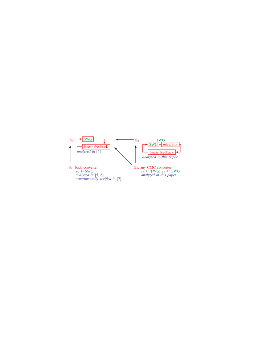
Figure 1: The systems 𝕊2subscript𝕊2\mathbb{S}_{2}, 𝕊3subscript𝕊3\mathbb{S}_{3} and 𝕊4subscript𝕊4\mathbb{S}_{4} can be converted to 𝕊1subscript𝕊1\mathbb{S}_{1} for further analysis.

For DC-DC converters with current mode control (CMC) or voltage mode control (VMC), subharmonic oscillation (fast-scale instability, FSI) may occur [1, 2]. The instability is common in peak CMC (PCMC), but rarely reported in average CMC (ACMC) [3].

Consider the following four closely related nonlinear systems:

  • 𝕊1subscript𝕊1\mathbb{S}_{1}:

    a square wave generator (SWG) with a linear feedback;

  • 𝕊2subscript𝕊2\mathbb{S}_{2}:

    a buck converter;

  • 𝕊3subscript𝕊3\mathbb{S}_{3}:

    a triangular wave generator (TWG) with a linear feedback; and

  • 𝕊4subscript𝕊4\mathbb{S}_{4}:

    any CMC converter.

The systems 𝕊2subscript𝕊2\mathbb{S}_{2}, 𝕊3subscript𝕊3\mathbb{S}_{3} and 𝕊4subscript𝕊4\mathbb{S}_{4} can be converted (denoted by “\to”) to 𝕊1subscript𝕊1\mathbb{S}_{1} as shown below (see also Fig. 1):

  • 𝕊2𝕊1subscript𝕊2subscript𝕊1\mathbb{S}_{2}\to\mathbb{S}_{1}:

    In the buck converter, the voltage vdsubscript𝑣𝑑v_{d} across the diode (or the second switch) is a square wave, then 𝕊2𝕊1subscript𝕊2subscript𝕊1\mathbb{S}_{2}\to\mathbb{S}_{1} [4, 5].

  • 𝕊3𝕊1subscript𝕊3subscript𝕊1\mathbb{S}_{3}\to\mathbb{S}_{1}:

    A TWG is equivalent to an SWG plus an integrator, and an integrator plus a linear feedback is still a linear feedback, then 𝕊3𝕊1subscript𝕊3subscript𝕊1\mathbb{S}_{3}\to\mathbb{S}_{1}.

  • 𝕊4𝕊1subscript𝕊4subscript𝕊1\mathbb{S}_{4}\to\mathbb{S}_{1}:

    In CMC, the inductor current iLsubscript𝑖𝐿i_{L} is a triangular wave (like an output of TWG), then 𝕊4𝕊3𝕊1subscript𝕊4subscript𝕊3subscript𝕊1\mathbb{S}_{4}\to\mathbb{S}_{3}\to\mathbb{S}_{1}, which makes a unified CMC model possible.

  • 𝕊4𝕊1subscript𝕊4subscript𝕊1\mathbb{S}_{4}\to\mathbb{S}_{1}:

    Also, the voltage vL=L(diL/dt)subscript𝑣𝐿𝐿𝑑subscript𝑖𝐿𝑑𝑡v_{L}=L(di_{L}/dt) across the inductor is a square wave, then 𝕊4𝕊1subscript𝕊4subscript𝕊1\mathbb{S}_{4}\to\mathbb{S}_{1}.

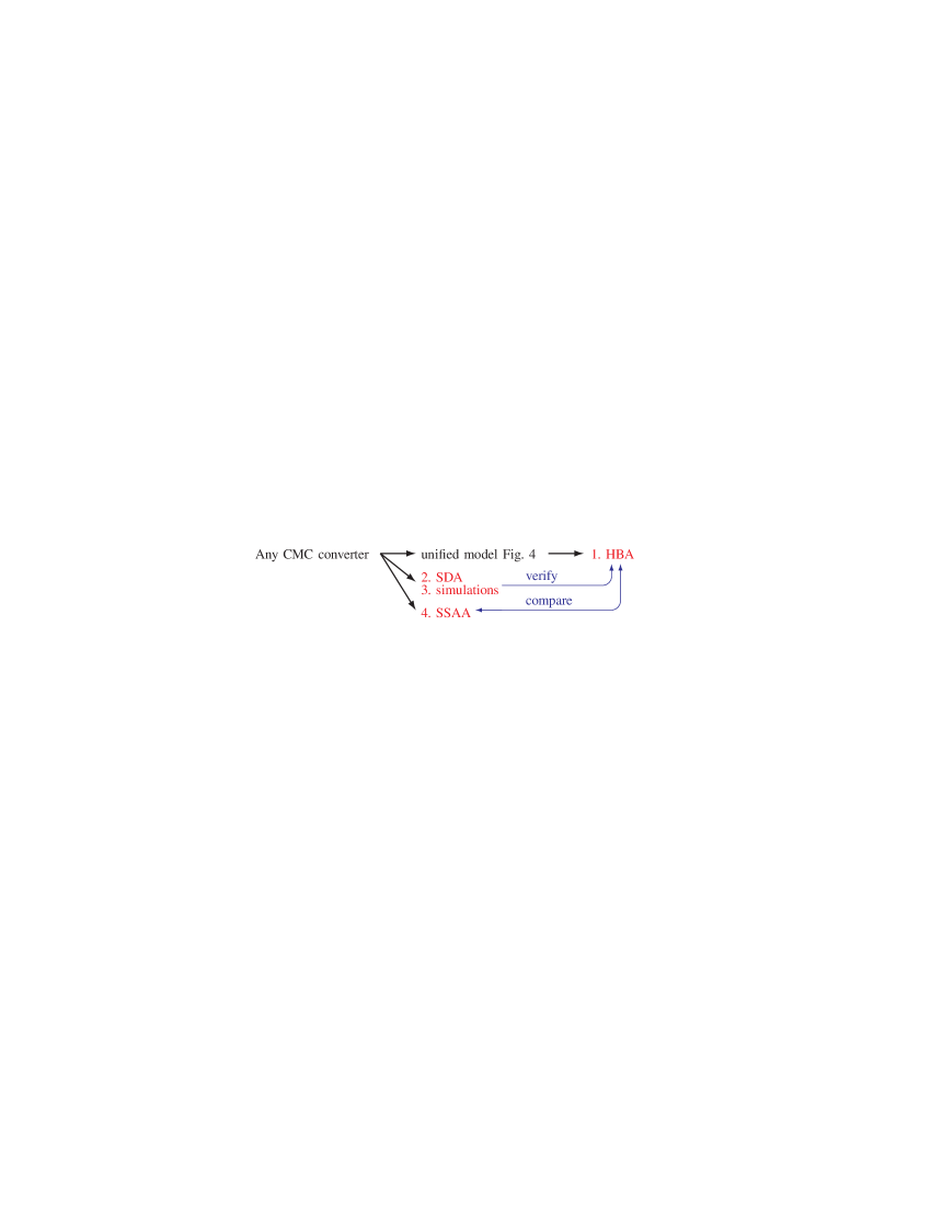
Although harmonic balance analysis (HBA) [4, 5, 6] has been applied to buck converters (𝕊2subscript𝕊2\mathbb{S}_{2} or 𝕊1subscript𝕊1\mathbb{S}_{1}) to obtain the FSI conditions, and experimentally verified in [7], its application to any CMC converter has not been reported. Based on the FSI conditions for 𝕊1subscript𝕊1\mathbb{S}_{1}, this paper derives the general FSI conditions for 𝕊3subscript𝕊3\mathbb{S}_{3} and 𝕊4subscript𝕊4\mathbb{S}_{4}. As shown in Fig. 2, all of the results are independently verified by time-domain simulations and sampled-data analysis (SDA) [8], a known accurate analysis for DC-DC converters. FSI occurs when a sampled-data (discrete-time) pole crosses -1. The results are also compared with state-space average analysis (SSAA) which is less accurate.
Refer to caption
Figure 2: Throughout the paper, the CMC converter is analyzed in four ways: it is first analyzed by HBA, independently verified by SDA and simulations, and then compared with SSAA.

This paper focuses on the FSI conditions and tries to answer the following questions:

  1. 1.

    The buck and boost converters have different dynamics. For example, the boost converter has a right half plane zero [9]. Do these two converters with CMC essentially have the same dynamics?

  2. 2.

    In the past research [10] on PCMC, a sampling effect is included in order to predict FSI, which requires increasing the system dimension. However, its application to ACMC has been questioned [11, 12]. Also, the ramp in PCMC is used for stabilization, whereas the ramp in ACMC is used for PWM modulation. Does a unified CMC model, applicable to both PCMC and ACMC, exist without increasing the system dimension?

  3. 3.

    Is the unified CMC model also applicable to buck, boost, and buck-boost converters?

  4. 4.

    A converter has many parameters. Each parameter has a different effect. Can these parameters be consolidated into a few parameters to predict FSI? Is there a single plot which predicts FSI?

The answers to these questions will be shown to be affirmative.

For PCMC with open voltage loop, the FSI conditions have been well reported. For ACMC [3, 11, 12, 13, 14, 15, 16, 17, 18, 19, 20], however, no accurate general closed-form FSI conditions have been reported. Also, the effects of the compensator poles and zeros on the stability have also not been reported. In this paper, the closed-form FSI conditions are derived, and the effects of many converter parameters can be clearly seen.

The remainder of the paper is organized as follows. The FSI conditions based on harmonic balance analysis [4] are reviewed in Section III. A unified CMC model is proposed in Section IV. It is then applied to various PCMC and ACMC schemes in Section V. The effect of the voltage loop ripple (at the output of the voltage-loop compensator) is considered in Section VI. Conclusions are collected in Section VII.

III Review of FSI Conditions Based on Harmonic Balance Analysis

FSI conditions based on harmonic balance analysis [4] are briefly reviewed. Consider a unity-gain SWG with a linear feedback. Denote the switching period as T𝑇T and the switching frequency as fs=1/Tsubscript𝑓𝑠1𝑇f_{s}=1/T, and let ωs=2πfssubscript𝜔𝑠2𝜋subscript𝑓𝑠\omega_{s}=2\pi f_{s}. Let the linear feedback transfer function be 𝒯(s)𝒯𝑠\mathcal{T}(s). Let ωpsubscript𝜔𝑝\omega_{p} be the pole and ωzsubscript𝜔𝑧\omega_{z} be the zero, for example. Let p=ωp/ωs𝑝subscript𝜔𝑝subscript𝜔𝑠p=\omega_{p}/\omega_{s} and z=ωz/ωs𝑧subscript𝜔𝑧subscript𝜔𝑠z=\omega_{z}/\omega_{s}. Let D𝐷D be the duty cycle. Take 𝒯(s)=ωs/(s+ωp)𝒯𝑠subscript𝜔𝑠𝑠subscript𝜔𝑝\mathcal{T}(s)=\omega_{s}/(s+\omega_{p}), for example. The stability condition (to avoid FSI) is α(D,p)<1𝛼𝐷𝑝1\alpha(D,p)<1, where

α(D,p)𝛼𝐷𝑝\displaystyle\alpha(D,p) =\displaystyle= 2πcsch(2πp)πeπp(12D)csch(πp)2𝜋csch2𝜋𝑝𝜋superscript𝑒𝜋𝑝12𝐷csch𝜋𝑝\displaystyle 2\pi\mathrm{csch}(2\pi p)-\pi e^{\pi p(1-2D)}\mathrm{csch}(\pi p)
:=assign\displaystyle:= k=0(1)kαk(D)pksuperscriptsubscript𝑘0superscript1𝑘subscript𝛼𝑘𝐷superscript𝑝𝑘\displaystyle\sum\limits_{k=0}^{\infty}(-1)^{k}\alpha_{k}(D)p^{k}
:=assign\displaystyle:= α0(D)α1(D)p+c(D,p)subscript𝛼0𝐷subscript𝛼1𝐷𝑝𝑐𝐷𝑝\displaystyle\alpha_{0}(D)-\alpha_{1}(D)p+c(D,p)
α0(D)subscript𝛼0𝐷\displaystyle\alpha_{0}(D) =\displaystyle= π(2D1)𝜋2𝐷1\displaystyle\pi(2D-1)
α1(D)subscript𝛼1𝐷\displaystyle\alpha_{1}(D) =\displaystyle= π2(2D22D+1)superscript𝜋22superscript𝐷22𝐷1\displaystyle\pi^{2}(2D^{2}-2D+1)

For other typical loop gains [4], see Table I. Based on partial fraction decomposition of 𝒯(s)𝒯𝑠\mathcal{T}(s), most FSI conditions are related with α(D,p)𝛼𝐷𝑝\alpha(D,p), which is a building block of other FSI conditions [4]. It is also the reason why a special form of α(D,p)𝛼𝐷𝑝\alpha(D,p) is defined as above.

Table I: Stability condition for typical loop gains 𝒯(s)𝒯𝑠\mathcal{T}(s) [4].
Case 𝒯(s)𝒯𝑠\mathcal{T}(s) Stability condition to avoid FSI
𝒞1subscript𝒞1\mathcal{C}_{1} 1s+ωp1𝑠subscript𝜔𝑝\frac{1}{s+\omega_{p}} 1ωsα(D,p)<11subscript𝜔𝑠𝛼𝐷𝑝1\frac{1}{\omega_{s}}\alpha(D,p)<1
𝒞2subscript𝒞2\mathcal{C}_{2} 1s1𝑠\frac{1}{s} 1ωsα0(D)<11subscript𝜔𝑠subscript𝛼0𝐷1\frac{1}{\omega_{s}}\alpha_{0}(D)<1
𝒞5subscript𝒞5\mathcal{C}_{5} 1s(1+s/ωp)1𝑠1𝑠subscript𝜔𝑝\frac{1}{s(1+s/\omega_{p})} 1ωs(α0(D)α(D,p))<11subscript𝜔𝑠subscript𝛼0𝐷𝛼𝐷𝑝1\frac{1}{\omega_{s}}(\alpha_{0}(D)-\alpha(D,p))<1
𝒞7subscript𝒞7\mathcal{C}_{7} 1+s/ωzs21𝑠subscript𝜔𝑧superscript𝑠2\frac{1+s/\omega_{z}}{s^{2}} 1ωs2(1zα0(D)+α1(D))<11superscriptsubscript𝜔𝑠21𝑧subscript𝛼0𝐷subscript𝛼1𝐷1\frac{1}{\omega_{s}^{2}}(\frac{1}{z}\alpha_{0}(D)+\alpha_{1}(D))<1
𝒞9subscript𝒞9\mathcal{C}_{9} 1+s/ωzs2(1+s/ωp)1𝑠subscript𝜔𝑧superscript𝑠21𝑠subscript𝜔𝑝\frac{1+s/\omega_{z}}{s^{2}(1+s/\omega_{p})} 1ωs2(α1(D)+(1p1z)(α(D,p)α0(D)))<11superscriptsubscript𝜔𝑠2subscript𝛼1𝐷1𝑝1𝑧𝛼𝐷𝑝subscript𝛼0𝐷1\frac{1}{\omega_{s}^{2}}(\alpha_{1}(D)+(\frac{1}{p}-\frac{1}{z})(\alpha(D,p)-\alpha_{0}(D)))<1

IV Unified PCMC/ACMC Model for Different Converters

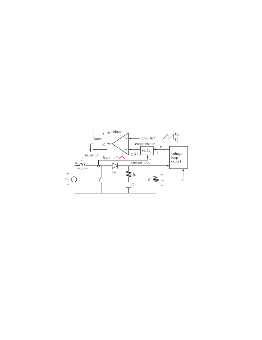
Consider a CMC boost converter shown in Fig. 3, where Gc(s)subscript𝐺𝑐𝑠G_{c}(s) is the current-loop compensator transfer function, Gv(s)subscript𝐺𝑣𝑠G_{v}(s) is the voltage-loop compensator transfer function, vssubscript𝑣𝑠v_{s} is the source voltage, vosubscript𝑣𝑜v_{o} is the output voltage, vcsubscript𝑣𝑐v_{c} is the control voltage, vrsubscript𝑣𝑟v_{r} is the reference voltage, Rssubscript𝑅𝑠R_{s} is sensing resistance, y𝑦y is a feedback signal, and hh is a PWM or compensating ramp varying from Vlsubscript𝑉𝑙V_{l} to Vhsubscript𝑉V_{h}. In Sections IV and V, vcsubscript𝑣𝑐v_{c} is assumed constant. The effect of voltage loop ripple is analyzed in Section VI. Let the equivalent series resistance (ESR) be Rcsubscript𝑅𝑐R_{c}. Denote the ramp slope as masubscript𝑚𝑎m_{a} and the ramp amplitude as Vm=VhVl=maTsubscript𝑉𝑚subscript𝑉subscript𝑉𝑙subscript𝑚𝑎𝑇V_{m}=V_{h}-V_{l}=m_{a}T.

Refer to caption
Figure 3: A CMC boost converter with a current-loop compensator Gc(s)subscript𝐺𝑐𝑠G_{c}(s) and a voltage-loop compensator Gv(s)subscript𝐺𝑣𝑠G_{v}(s).

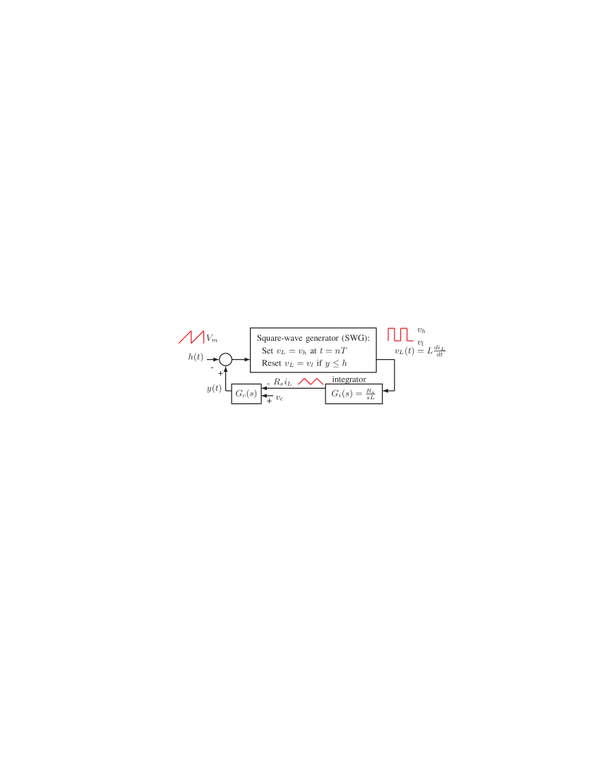
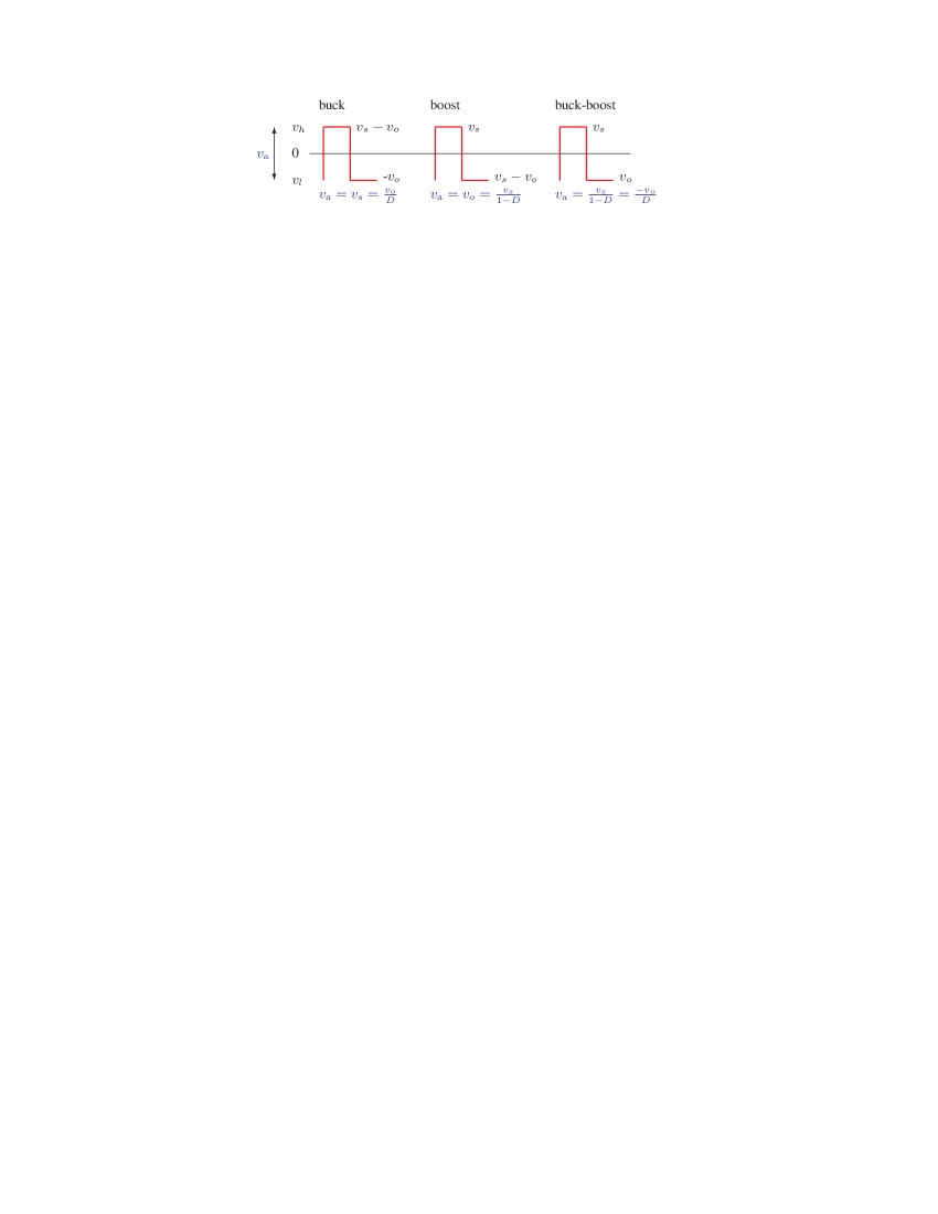
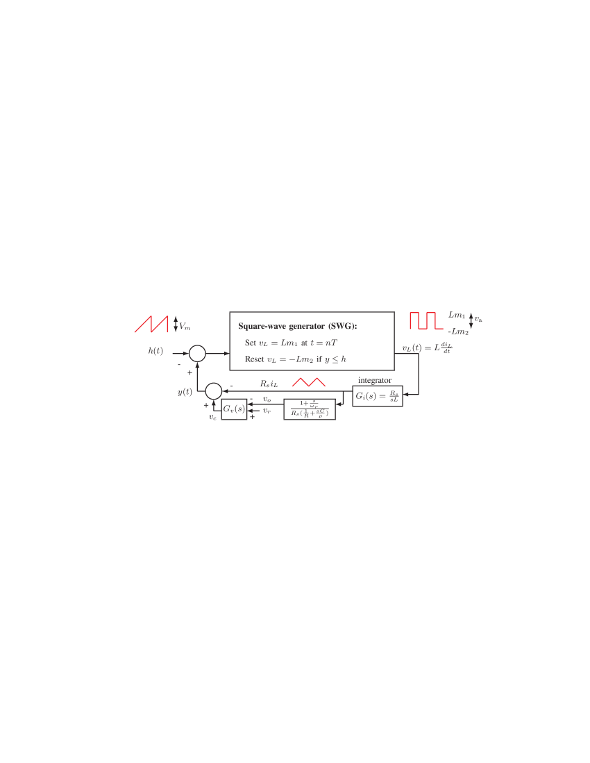
The inductor current iLsubscript𝑖𝐿i_{L} is a triangular wave, and and the voltage across the inductor vL(t)=LdiL/dtsubscript𝑣𝐿𝑡𝐿𝑑subscript𝑖𝐿𝑑𝑡v_{L}(t)=Ldi_{L}/dt is a square wave. Therefore, a CMC converter can be represented by a unified model shown in Fig. 4. Let the square wave vL(t)subscript𝑣𝐿𝑡v_{L}(t) have a high value vhsubscript𝑣v_{h}, a low value vlsubscript𝑣𝑙v_{l}, and an amplitude va=vhvlsubscript𝑣asubscript𝑣subscript𝑣𝑙v_{\mathrm{a}}=v_{h}-v_{l}, as shown in Fig. 5 for different converters. Take the boost converter, for example. When the switch is on, LdiL/dt=vs𝐿𝑑subscript𝑖𝐿𝑑𝑡subscript𝑣𝑠Ldi_{L}/dt=v_{s}. When the switch is off, LdiL/dt=vsvo𝐿𝑑subscript𝑖𝐿𝑑𝑡subscript𝑣𝑠subscript𝑣𝑜Ldi_{L}/dt=v_{s}-v_{o}. Then, va=vs(vsvo)=vo=vs/(1D)subscript𝑣asubscript𝑣𝑠subscript𝑣𝑠subscript𝑣𝑜subscript𝑣𝑜subscript𝑣𝑠1𝐷v_{\mathrm{a}}=v_{s}-(v_{s}-v_{o})=v_{o}=v_{s}/(1-D). Denote |i˙L|subscript˙𝑖𝐿|\dot{i}_{L}| by m1subscript𝑚1m_{1} and m2subscript𝑚2m_{2} when the (first) switch is on and off, respectively. Then vh=Lm1subscript𝑣𝐿subscript𝑚1v_{h}=Lm_{1}, vl=Lm2subscript𝑣𝑙𝐿subscript𝑚2v_{l}=-Lm_{2}, va=L(m1+m2)subscript𝑣a𝐿subscript𝑚1subscript𝑚2v_{\mathrm{a}}=L(m_{1}+m_{2}) which is another universal expression of vasubscript𝑣av_{\mathrm{a}}.

Refer to caption
Figure 4: Unified CMC model, applicable to PCMC/ACMC buck, boost, and buck-boost converters, for example.
Refer to caption
Figure 5: The waveform of vL(t)=Li˙Lsubscript𝑣𝐿𝑡𝐿subscript˙𝑖𝐿v_{L}(t)=L\dot{i}_{L} for different converters.

V Applications to PCMC and ACMC

In Fig. 4, the SWG contributes a gain va/Vmsubscript𝑣asubscript𝑉𝑚v_{\mathrm{a}}/V_{m}, then the (current) loop gain 𝒯(s)=vaGc(s)Gi(s)/Vm𝒯𝑠subscript𝑣asubscript𝐺𝑐𝑠subscript𝐺𝑖𝑠subscript𝑉𝑚\mathcal{T}(s)=v_{\mathrm{a}}G_{c}(s)G_{i}(s)/V_{m}. Different CMC schemes have different Gc(s)subscript𝐺𝑐𝑠G_{c}(s), 𝒯(s)𝒯𝑠\mathcal{T}(s) and stability conditions (summarized in Table II), which will be verified by time-domain simulations (summarized in Table III).

V-A PCMC: Case 𝒞2subscript𝒞2\mathcal{C}_{2}

In PCMC, y=vcRsiL𝑦subscript𝑣𝑐subscript𝑅𝑠subscript𝑖𝐿y=v_{c}-R_{s}i_{L}, Gc(s)=1subscript𝐺𝑐𝑠1G_{c}(s)=1 and 𝒯(s)=vaGi(s)/Vm=vaRs/sVmL𝒯𝑠subscript𝑣asubscript𝐺𝑖𝑠subscript𝑉𝑚subscript𝑣asubscript𝑅𝑠𝑠subscript𝑉𝑚𝐿\mathcal{T}(s)=v_{\mathrm{a}}G_{i}(s)/V_{m}=v_{\mathrm{a}}R_{s}/sV_{m}L which belongs to case 𝒞2subscript𝒞2\mathcal{C}_{2}. Let 𝒮𝒮\mathcal{S} be an S-plot [4] to show the required stabilizing ramp slope. For 𝒮<ma𝒮subscript𝑚𝑎\mathcal{S}<m_{a}, the converter is stable. From Table I, the stability condition is

vaRsα0(D)VmLωs<1or𝒮:=vaRs(D0.5)L<masubscript𝑣asubscript𝑅𝑠subscript𝛼0𝐷subscript𝑉𝑚𝐿subscript𝜔𝑠1or𝒮assignsubscript𝑣asubscript𝑅𝑠𝐷0.5𝐿subscript𝑚𝑎\frac{v_{\mathrm{a}}R_{s}\alpha_{0}(D)}{V_{m}L\omega_{s}}<1\hskip 8.53581pt\mbox{or}\hskip 8.53581pt\mathcal{S}:=\frac{v_{\mathrm{a}}R_{s}(D-0.5)}{L}<m_{a} (1)

where va=vssubscript𝑣asubscript𝑣𝑠v_{\mathrm{a}}=v_{s} for buck converters and va=vs/(1D)subscript𝑣asubscript𝑣𝑠1𝐷v_{\mathrm{a}}=v_{s}/(1-D) for boost or buck-boost converters, agreed with [21].

Table II: Unified stability conditions (in terms of ramp slope masubscript𝑚𝑎m_{a}) for different CMC schemes, applicable to any CMC converter.
PCMC                     𝒮:=vaRsL(D12)<maassign𝒮subscript𝑣asubscript𝑅𝑠𝐿𝐷12subscript𝑚𝑎\mathcal{S}:=\frac{v_{\mathrm{a}}R_{s}}{L}(D-\frac{1}{2})<m_{a}
ACMC (type-II)          𝒮:=vaRsKcTLωs2((α1(D)+(1p1z)(α(D,p)α0(D))))<maassign𝒮subscript𝑣asubscript𝑅𝑠subscript𝐾𝑐𝑇𝐿superscriptsubscript𝜔𝑠2subscript𝛼1𝐷1𝑝1𝑧𝛼𝐷𝑝subscript𝛼0𝐷subscript𝑚𝑎\mathcal{S}:=\frac{v_{\mathrm{a}}R_{s}K_{c}}{TL\omega_{s}^{2}}((\alpha_{1}(D)+(\frac{1}{p}-\frac{1}{z})(\alpha(D,p)-\alpha_{0}(D))))<m_{a}
          (for ωzωsmuch-less-thansubscript𝜔𝑧subscript𝜔𝑠\omega_{z}\ll\omega_{s})     𝒮:=vaRsKcTωzLωs(α0(D)α(D,p))<maassign𝒮subscript𝑣asubscript𝑅𝑠subscript𝐾𝑐𝑇subscript𝜔𝑧𝐿subscript𝜔𝑠subscript𝛼0𝐷𝛼𝐷𝑝subscript𝑚𝑎\mathcal{S}:=\frac{v_{\mathrm{a}}R_{s}K_{c}}{T\omega_{z}L\omega_{s}}(\alpha_{0}(D)-\alpha(D,p))<m_{a}
          (for ωzωsmuch-less-thansubscript𝜔𝑧subscript𝜔𝑠\omega_{z}\ll\omega_{s})     K:=vaRsKcVmωzLωs<Kmax(D,p):=1α0(D)α(D,p)assign𝐾subscript𝑣asubscript𝑅𝑠subscript𝐾𝑐subscript𝑉𝑚subscript𝜔𝑧𝐿subscript𝜔𝑠subscript𝐾max𝐷𝑝assign1subscript𝛼0𝐷𝛼𝐷𝑝K:=\frac{v_{\mathrm{a}}R_{s}K_{c}}{V_{m}\omega_{z}L\omega_{s}}<K_{\mathrm{max}}(D,p):=\frac{1}{\alpha_{0}(D)-\alpha(D,p)}
ACMC (PI)               𝒮:=vaRsKcL(2D12ωz+(12D+2D2)T4)<maassign𝒮subscript𝑣asubscript𝑅𝑠subscript𝐾𝑐𝐿2𝐷12subscript𝜔𝑧12𝐷2superscript𝐷2𝑇4subscript𝑚𝑎\mathcal{S}:=\frac{v_{\mathrm{a}}R_{s}K_{c}}{L}(\frac{2D-1}{2\omega_{z}}+\frac{(1-2D+2D^{2})T}{4})<m_{a}
                               K:=vaRsKcVmLωs2<Kmax(D,z):=1α0(D)/z+α1(D)assignKsubscript𝑣asubscript𝑅𝑠subscript𝐾𝑐subscript𝑉𝑚𝐿superscriptsubscript𝜔𝑠2subscriptKmax𝐷𝑧assign1subscript𝛼0𝐷𝑧subscript𝛼1𝐷\mathrm{K}:=\frac{v_{\mathrm{a}}R_{s}K_{c}}{V_{m}L\omega_{s}^{2}}<\mathrm{K}_{\mathrm{max}}(D,z):=\frac{1}{\alpha_{0}(D)/z+\alpha_{1}(D)}
Note: va=vssubscript𝑣asubscript𝑣𝑠v_{\mathrm{a}}=v_{s} for buck converters and va=vs/(1D)subscript𝑣asubscript𝑣𝑠1𝐷v_{\mathrm{a}}=v_{s}/(1-D) for boost or buck-boost converters.
Table III: Stable/unstable boost converters in Examples 1-3.
Ex. K𝐾K or KK\mathrm{K} D p𝑝p or z𝑧z Stability In parameter space Simulation PM
1 K=0.4𝐾0.4K=0.4 0.86 p=0.75𝑝0.75p=0.75 unstable [a] in Figs. 7(d) & 6(d) Fig. 8 60superscript6060^{\circ}
K=0.4𝐾0.4K=0.4 0.85 p=0.75𝑝0.75p=0.75 stable [b] in Fig. 7(d) Fig. 10
2 K=1.3𝐾1.3K=1.3 0.36 p=0.17𝑝0.17p=0.17 stable [c] in Fig. 7(c) Fig. 11
K=1.3𝐾1.3K=1.3 0.36 p=0.18𝑝0.18p=0.18 unstable [d] in Figs. 7(c) & 6(c) Fig. 12 18superscript1818^{\circ}
K=1.3𝐾1.3K=1.3 0.36 p=0.515𝑝0.515p=0.515 unstable [e] in Figs. 7(c) & 6(c) Fig. 14 33superscript3333^{\circ}
K=1.3𝐾1.3K=1.3 0.36 p=0.52𝑝0.52p=0.52 stable [f] in Fig. 7(c) Fig. 16
3 K=0.0232K0.0232\mathrm{K}=0.0232 0.6 z=0.018𝑧0.018z=0.018 unstable [g] in Figs. 19(c) & 23 Fig. 20 89superscript8989^{\circ}
K=0.0232K0.0232\mathrm{K}=0.0232 0.58 z=0.018𝑧0.018z=0.018 stable [h] in Figs. 19(c) & 23 Fig. 22

V-B ACMC with Type-II Compensator: Case 𝒞5subscript𝒞5\mathcal{C}_{5} or 𝒞9subscript𝒞9\mathcal{C}_{9}

For ACMC, y=Gc(s)(vcRsiL)+vc𝑦subscript𝐺𝑐𝑠subscript𝑣𝑐subscript𝑅𝑠subscript𝑖𝐿subscript𝑣𝑐y=G_{c}(s)(v_{c}-R_{s}i_{L})+v_{c}, which has an additional offset vcsubscript𝑣𝑐v_{c} but does not affect the loop gain. Let the type-II phase-lead compensator (with ωz<ωpsubscript𝜔𝑧subscript𝜔𝑝\omega_{z}<\omega_{p}) be

Gc(s)=Kc(1+s/ωz)s(1+s/ωp)subscript𝐺𝑐𝑠subscript𝐾𝑐1𝑠subscript𝜔𝑧𝑠1𝑠subscript𝜔𝑝G_{c}(s)=\frac{K_{c}(1+s/\omega_{z})}{s(1+s/\omega_{p})} (2)

where Kcsubscript𝐾𝑐K_{c} is a gain. Generally, ωzωsmuch-less-thansubscript𝜔𝑧subscript𝜔𝑠\omega_{z}\ll\omega_{s}. Let K=vaRsKc/VmωzLωs𝐾subscript𝑣asubscript𝑅𝑠subscript𝐾𝑐subscript𝑉𝑚subscript𝜔𝑧𝐿subscript𝜔𝑠K=v_{\mathrm{a}}R_{s}K_{c}/V_{m}\omega_{z}L\omega_{s}. Then

𝒯(s)𝒯𝑠\displaystyle\mathcal{T}(s) =\displaystyle= vaGc(s)Gi(s)Vm=vaRsKc(1+sωz)VmLs2(1+sωp)subscript𝑣asubscript𝐺𝑐𝑠subscript𝐺𝑖𝑠subscript𝑉𝑚subscript𝑣asubscript𝑅𝑠subscript𝐾𝑐1𝑠subscript𝜔𝑧subscript𝑉𝑚𝐿superscript𝑠21𝑠subscript𝜔𝑝\displaystyle\frac{v_{\mathrm{a}}G_{c}(s)G_{i}(s)}{V_{m}}=\frac{v_{\mathrm{a}}R_{s}K_{c}(1+\frac{s}{\omega_{z}})}{V_{m}Ls^{2}(1+\frac{s}{\omega_{p}})} (3)
\displaystyle\approx Kωss(1+sωp) (at frequency ωsωz)𝐾subscript𝜔𝑠𝑠1𝑠subscript𝜔𝑝 (at frequency ωsωz)\displaystyle\frac{K\omega_{s}}{s(1+\frac{s}{\omega_{p}})}\hskip 14.22636pt\mbox{ (at frequency $\omega_{s}\gg\omega_{z}$)} (4)

V-B1 Based on SSAA: Converter is expected to be stable

Let ωcsubscript𝜔𝑐\omega_{c} be the crossover frequency. Setting |𝒯(jωc)|=1𝒯𝑗subscript𝜔𝑐1|\mathcal{T}(j\omega_{c})|=1 in (4) leads to

ωcsubscript𝜔𝑐\displaystyle\omega_{c} =\displaystyle= ωs2p4+4K2p2p2subscript𝜔𝑠2superscript𝑝44superscript𝐾2superscript𝑝2superscript𝑝2\displaystyle\frac{\omega_{s}}{\sqrt{2}}\sqrt{\sqrt{p^{4}+4K^{2}p^{2}}-p^{2}} (5)
\displaystyle\approx {ωsK (for Kp)ωsKp (for Kpcasessubscript𝜔𝑠𝐾 (for Kp)missing-subexpressionsubscript𝜔𝑠𝐾𝑝 (for Kp\displaystyle\left\{\begin{array}[]{l}\omega_{s}K\hskip 14.22636pt\mbox{ (for $K\ll p$)}\\ \\ \omega_{s}\sqrt{Kp}\hskip 14.22636pt\mbox{ (for $K\gg p$) }\end{array}\right. (9)

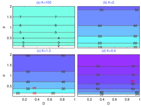
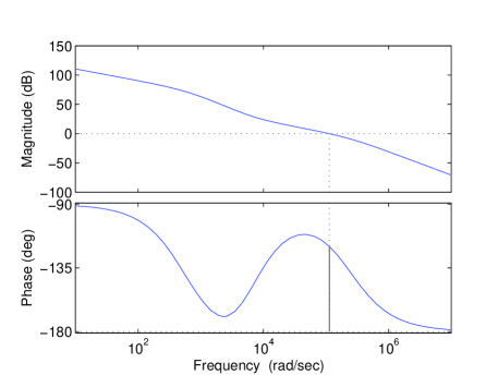
A large K𝐾K leads to a large ωcsubscript𝜔𝑐\omega_{c}. From (4), the phase margin (PM) is 90arctan(ωc/ωp)>0superscript90subscript𝜔𝑐subscript𝜔𝑝090^{\circ}-\arctan(\omega_{c}/\omega_{p})>0. PM is a function of K𝐾K and p𝑝p, independent of D𝐷D. For K=100𝐾100K=100, 2, 1.3, and 0.4, the plots of PM in the (D,p)𝐷𝑝(D,p) space are shown in Fig. 6, and the converter is expected to be always stable. As K𝐾K decreases, ωcsubscript𝜔𝑐\omega_{c} decreases and PM increases.

V-B2 Based on HBA: FSI may occur even with PM >0absent0>0

From (4), 𝒯(s)𝒯𝑠\mathcal{T}(s) belongs to case 𝒞5subscript𝒞5\mathcal{C}_{5} in Table I, and the stability condition to avoid FSI is

K(α0(D)α(D,p))<1𝐾subscript𝛼0𝐷𝛼𝐷𝑝1K(\alpha_{0}(D)-\alpha(D,p))<1 (10)

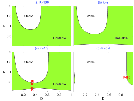
which can be expressed in terms of the required ramp slope masubscript𝑚𝑎m_{a}, as shown in Table II. FSI may occur if (10) is not met. For the same K𝐾K as in Fig. 6, the stable regions according to (10) are shown in Fig. 7. As K𝐾K decreases, the stability region enlarges, but there still exist instability regions. From [5], no subharmonic oscillation occurs if K<1/π𝐾1𝜋K<1/\pi, which is a conservative condition and it is approximately equivalent to ωc<ωs/πsubscript𝜔𝑐subscript𝜔𝑠𝜋\omega_{c}<\omega_{s}/\pi according to (9). A large ωcsubscript𝜔𝑐\omega_{c} leads to FSI. However, such a condition ωc<ωs/πsubscript𝜔𝑐subscript𝜔𝑠𝜋\omega_{c}<\omega_{s}/\pi may be too conservative. The converter can be designed according to the limit (10) with larger ωcsubscript𝜔𝑐\omega_{c} for higher performance without losing stability.

Note that PM in Fig. 6 is independent of D𝐷D, whereas the stability in Fig. 7 depends on D𝐷D. Comparing Fig. 7 with Fig. 6, one sees that the converter may be unstable even with PM = 60superscript6060^{\circ}, for example, if K=0.4𝐾0.4K=0.4, D=0.86𝐷0.86D=0.86, and p=0.75𝑝0.75p=0.75 as shown in the next example.

Refer to caption
Figure 6: As K𝐾K decreases, PM increases, independent of D𝐷D, but FSI still occurs as shown in Fig. 7, different colors for different PM.
Refer to caption
Figure 7: As K𝐾K decreases, the instability region still exists but shrinks.

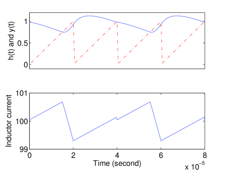
Example 1. (FSI with PM = 60superscript6060^{\circ}.) Consider an ACMC boost converter (adapted from the buck converter in [5]) with a type-II compensator: vo=14subscript𝑣𝑜14v_{o}=14 V, Vm=1subscript𝑉𝑚1V_{m}=1 V, fs=50subscript𝑓𝑠50f_{s}=50 kHz, L=46.1𝐿46.1L=46.1 μ𝜇\muH, C=380𝐶380C=380 μ𝜇\muF, Rc=0.02subscript𝑅𝑐0.02R_{c}=0.02 ΩΩ\Omega, Rs=16.4subscript𝑅𝑠16.4R_{s}=16.4 mΩΩ\Omega, R=1𝑅1R=1 ΩΩ\Omega, ωz=5652.9subscript𝜔𝑧5652.9\omega_{z}=5652.9 rad/s, p=0.75𝑝0.75p=0.75, Kc=141670subscript𝐾𝑐141670K_{c}=141670, and K=0.4𝐾0.4K=0.4.

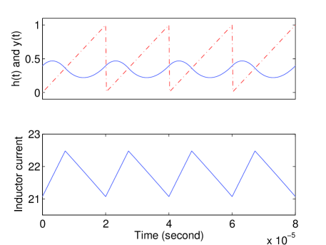
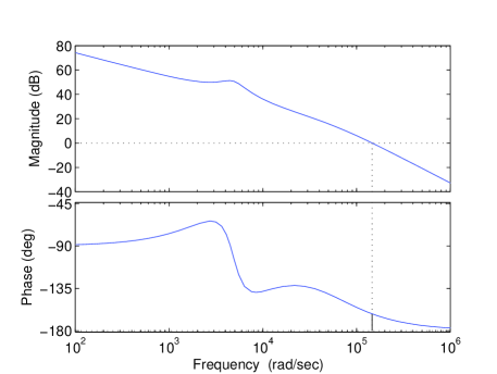
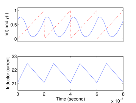
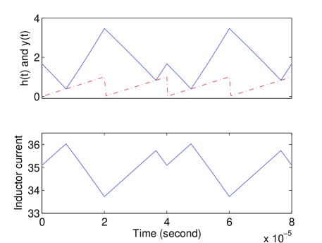
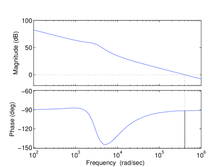
First, let vs=1.96subscript𝑣𝑠1.96v_{s}=1.96 V and vc=1.64subscript𝑣𝑐1.64v_{c}=1.64 V. Here, D=0.86𝐷0.86D=0.86. The converter is unstable (Fig. 8) although its average model has PM = 60superscript6060^{\circ} (Fig. 9). The linear average model is too simple to predict the FSI of the nonlinear converter. Independent sampled-data analysis also shows an unstable pole at -1.02, and three stable poles at 0, 0.88, and 0.91, thus verifying the instability.

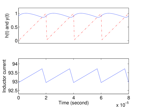
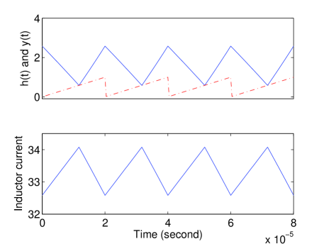
Next, let vs=2.1subscript𝑣𝑠2.1v_{s}=2.1 V and vc=1.53subscript𝑣𝑐1.53v_{c}=1.53 V. Now, D=0.85𝐷0.85D=0.85. The converter is stable (Fig. 10). In Fig. 7(d), for K=0.4𝐾0.4K=0.4, draw a line at p=0.75𝑝0.75p=0.75. The instability occurs indeed around D=0.86𝐷0.86D=0.86. \Box

Refer to caption
Figure 8: The boost converter is unstable, vs=1.96subscript𝑣𝑠1.96v_{s}=1.96 V.
Refer to caption
Figure 9: The loop gain 𝒯(jω)𝒯𝑗𝜔\mathcal{T}(j\omega) has PM = 60superscript6060^{\circ}, vs=1.96subscript𝑣𝑠1.96v_{s}=1.96 V.
Refer to caption
Figure 10: The boost converter is stable, vs=2.1subscript𝑣𝑠2.1v_{s}=2.1 V.

As reported in [5], the ACMC buck converter may have an unstable window of p𝑝p. The next example shows that the boost converter also has the same unstable window.

Example 2. (Unstable window of p𝑝p in the boost converter, adapted from the buck converter in [5].) Continue from Example 1, but with vs=9subscript𝑣𝑠9v_{s}=9 V, vc=0.357subscript𝑣𝑐0.357v_{c}=0.357 V, and Kc=460420subscript𝐾𝑐460420K_{c}=460420. This boost converter example is actually adapted from Example 3 of [5] for a buck converter, where an unstable window of p𝑝p was found. This example also illustrates the buck and boost converters, known to have different dynamics, have the same occurrence of FSI with the same parameters. Both examples have the same va=14subscript𝑣a14v_{\mathrm{a}}=14 V, where va=vssubscript𝑣asubscript𝑣𝑠v_{\mathrm{a}}=v_{s} for the buck converter and va=vosubscript𝑣asubscript𝑣𝑜v_{\mathrm{a}}=v_{o} for the boost converter. Both examples also have the same D=0.36𝐷0.36D=0.36 and K=1.3𝐾1.3K=1.3 (and also other parameters such as R𝑅R, L𝐿L, C𝐶C, Rcsubscript𝑅𝑐R_{c}, and ωzsubscript𝜔𝑧\omega_{z}). Therefore, an unstable window of p𝑝p for this boost converter is also expected. In Fig. 7(c), for K=1.3𝐾1.3K=1.3, draw a line at D=0.36𝐷0.36D=0.36, which shows an unstable window of p[0.18,0.515]𝑝0.180.515p\in[0.18,0.515]. For p<0.18𝑝0.18p<0.18 or p>0.515𝑝0.515p>0.515, the converter is stable.

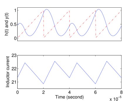
First, let p=0.17𝑝0.17p=0.17. The converter is stable (Fig. 11).

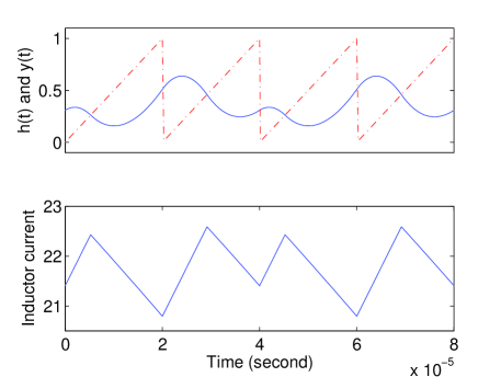
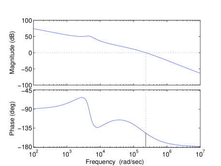
Second, let p=0.18𝑝0.18p=0.18. The converter is unstable (Fig. 12) although its average model has PM = 18superscript1818^{\circ} (Fig. 13). Independent sampled-data analysis shows an unstable pole at -1.07, and three stable poles at 0.35, 0.88, and 0.91.

Third, let p=0.515𝑝0.515p=0.515. The converter is unstable (Fig. 14) although its average model has PM = 33superscript3333^{\circ} (Fig. 15). Independent sampled-data analysis shows an unstable pole at -1.002, and three stable poles at -0.05, 0.88, and 0.91.

Fourth, let p=0.52𝑝0.52p=0.52. The converter is stable again (Fig. 16). The boost converter indeed has an unstable window of p[0.18,0.515]𝑝0.180.515p\in[0.18,0.515], same as the buck converter in [5]. \Box
Refer to caption
Figure 11: The boost converter is stable, p=0.17𝑝0.17p=0.17.
Refer to caption
Figure 12: The boost converter is unstable, p=0.18𝑝0.18p=0.18.
Refer to caption
Figure 13: The loop gain 𝒯(jω)𝒯𝑗𝜔\mathcal{T}(j\omega) has PM = 18superscript1818^{\circ}, p=0.18𝑝0.18p=0.18.
Refer to caption
Figure 14: The boost converter is unstable, p=0.515𝑝0.515p=0.515.
Refer to caption
Figure 15: The loop gain 𝒯(jω)𝒯𝑗𝜔\mathcal{T}(j\omega) has PM = 33superscript3333^{\circ}, p=0.515𝑝0.515p=0.515.
Refer to caption
Figure 16: The boost converter is stable, p=0.52𝑝0.52p=0.52.

Note that K=vaRsKc/VmωzLωs𝐾subscript𝑣asubscript𝑅𝑠subscript𝐾𝑐subscript𝑉𝑚subscript𝜔𝑧𝐿subscript𝜔𝑠K=v_{\mathrm{a}}R_{s}K_{c}/V_{m}\omega_{z}L\omega_{s}, and one can see the effect of each parameter on the stability. The condition (10) can be expressed in terms of the required ramp slope masubscript𝑚𝑎m_{a}, as shown in Table II:

ma>𝒮:=voRsKc2πωzL(α0(D)α(D,p))subscript𝑚𝑎𝒮assignsubscript𝑣𝑜subscript𝑅𝑠subscript𝐾𝑐2𝜋subscript𝜔𝑧𝐿subscript𝛼0𝐷𝛼𝐷𝑝m_{a}>\mathcal{S}:=\frac{v_{o}R_{s}K_{c}}{2\pi\omega_{z}L}(\alpha_{0}(D)-\alpha(D,p)) (11)

The condition (10) can be also expressed in terms of K𝐾K:

K<1α0(D)α(D,p):=Kmax(D,p)𝐾1subscript𝛼0𝐷𝛼𝐷𝑝assignsubscript𝐾max𝐷𝑝K<\frac{1}{\alpha_{0}(D)-\alpha(D,p)}:=K_{\mathrm{max}}(D,p) (12)

if Kmax(D,p)subscript𝐾max𝐷𝑝K_{\mathrm{max}}(D,p) is positive. If Kmax(D,p)subscript𝐾max𝐷𝑝K_{\mathrm{max}}(D,p) is negative, the converter is always stable (because the inequality sign in (12) is reversed and the condition (12) is always met).

For the boost converter, va=vosubscript𝑣asubscript𝑣𝑜v_{\mathrm{a}}=v_{o} which is fixed (if regulated), and (12) becomes

K=voRsKcVmωzLωs<Kmax(D,p)𝐾subscript𝑣𝑜subscript𝑅𝑠subscript𝐾𝑐subscript𝑉𝑚subscript𝜔𝑧𝐿subscript𝜔𝑠subscript𝐾max𝐷𝑝K=\frac{v_{o}R_{s}K_{c}}{V_{m}\omega_{z}L\omega_{s}}<K_{\mathrm{max}}(D,p) (13)

In [11, Eq. 14], a conservative condition was proposed:

voRsKcVmωzLωs<min[1π(1D),12π]=12πsubscript𝑣𝑜subscript𝑅𝑠subscript𝐾𝑐subscript𝑉𝑚subscript𝜔𝑧𝐿subscript𝜔𝑠1𝜋1𝐷12𝜋12𝜋\frac{v_{o}R_{s}K_{c}}{V_{m}\omega_{z}L\omega_{s}}<\min[\frac{1}{\pi(1-D)},\frac{1}{2\pi}]=\frac{1}{2\pi} (14)

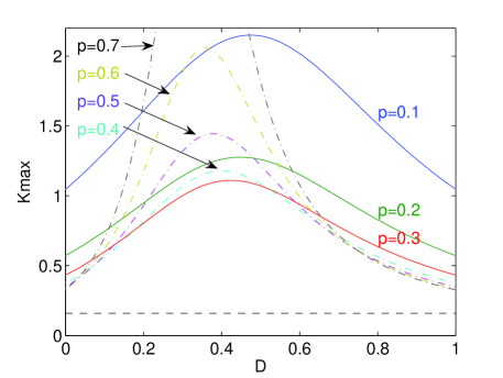
where the effect of p𝑝p was neglected. The plots of (14) and Kmax(D,p)subscript𝐾max𝐷𝑝K_{\mathrm{max}}(D,p) for different values of p𝑝p are shown in Fig. 17.

The plot of Kmax(D,p)subscript𝐾max𝐷𝑝K_{\mathrm{max}}(D,p) is quite nonlinear. As p𝑝p increases from 0.1 to 0.3, Kmax(D,p)subscript𝐾max𝐷𝑝K_{\mathrm{max}}(D,p) decreases, whereas as p𝑝p increases from 0.4 to 0.7 (and beyond), Kmax(D,p)subscript𝐾max𝐷𝑝K_{\mathrm{max}}(D,p) increases. It indicates that around p=0.3𝑝0.3p=0.3 the stability region shrinks, agreed with Fig. 7 which also indicates a possible unstable window of p𝑝p. One sees that the condition (14) reported in [11] is conservative because Kmax(D,p)>1/2πsubscript𝐾max𝐷𝑝12𝜋K_{\mathrm{max}}(D,p)>1/2\pi as shown in Fig. 17.

As indicated in Fig. 17, the converter is prone to be stable around D=0.4𝐷0.4D=0.4 (than other values of D𝐷D), also agreed with Fig. 7. The closed-form Kmax(D,p)subscript𝐾max𝐷𝑝K_{\mathrm{max}}(D,p) is such nonlinear that it is difficult to further simplify it. Instead, one can make the plot of Kmax(D,p)subscript𝐾max𝐷𝑝K_{\mathrm{max}}(D,p) to predict the stability.

Since a single K=vaRsKc/VmωzLωs𝐾subscript𝑣asubscript𝑅𝑠subscript𝐾𝑐subscript𝑉𝑚subscript𝜔𝑧𝐿subscript𝜔𝑠K=v_{\mathrm{a}}R_{s}K_{c}/V_{m}\omega_{z}L\omega_{s} contains many design parameters, the plot of Kmax(D,p)subscript𝐾max𝐷𝑝K_{\mathrm{max}}(D,p) is very useful to design a stable converter. Given the values of p𝑝p and the ranges of D𝐷D, one can make a plot of Kmax(D,p)subscript𝐾max𝐷𝑝K_{\mathrm{max}}(D,p) and adjust different parameters so that the condition K<Kmax(D,p)𝐾subscript𝐾max𝐷𝑝K<K_{\mathrm{max}}(D,p) is met.

For the buck converter, va=vs=vo/Dsubscript𝑣asubscript𝑣𝑠subscript𝑣𝑜𝐷v_{\mathrm{a}}=v_{s}=v_{o}/D and (12) becomes

voRsKcVmωzLωs<DKmax(D,p)subscript𝑣𝑜subscript𝑅𝑠subscript𝐾𝑐subscript𝑉𝑚subscript𝜔𝑧𝐿subscript𝜔𝑠𝐷subscript𝐾max𝐷𝑝\frac{v_{o}R_{s}K_{c}}{V_{m}\omega_{z}L\omega_{s}}<DK_{\mathrm{max}}(D,p) (15)

In [11, Eq. 13], a conservative condition was proposed:

voRsKcVmωzLωs<min[Dπ(1D),12π]subscript𝑣𝑜subscript𝑅𝑠subscript𝐾𝑐subscript𝑉𝑚subscript𝜔𝑧𝐿subscript𝜔𝑠𝐷𝜋1𝐷12𝜋\frac{v_{o}R_{s}K_{c}}{V_{m}\omega_{z}L\omega_{s}}<\min[\frac{D}{\pi(1-D)},\frac{1}{2\pi}] (16)

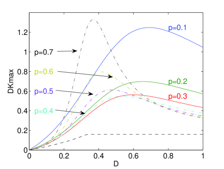
The plots of (16) and DKmax(D,p)𝐷subscript𝐾max𝐷𝑝DK_{\mathrm{max}}(D,p) for different values of p𝑝p are shown in Fig. 18. As p𝑝p increases from 0.1 to 0.3, DKmax(D,p)𝐷subscript𝐾max𝐷𝑝DK_{\mathrm{max}}(D,p) decreases. As p𝑝p increases from 0.4 to 0.7, DKmax(D,p)𝐷subscript𝐾max𝐷𝑝DK_{\mathrm{max}}(D,p) increases. One sees that the condition (16) reported in [11] is also conservative. From Fig. 18, the buck converter is susceptible to FSI if D𝐷D is too small.

Refer to caption
Figure 17: The plots of Kmax(D,p)subscript𝐾max𝐷𝑝K_{\mathrm{max}}(D,p) for the boost converter, dashed line for the conservative condition (14).
Refer to caption
Figure 18: The plots of DKmax(D,p)𝐷subscript𝐾max𝐷𝑝DK_{\mathrm{max}}(D,p) for the buck converter, dashed line for the conservative condition (16).

In the above analysis, ωzωsmuch-less-thansubscript𝜔𝑧subscript𝜔𝑠\omega_{z}\ll\omega_{s} is assumed. If that is not the case, the loop gain (3) belongs to case 𝒞9subscript𝒞9\mathcal{C}_{9}. Based on Table I, the (general) stability condition is

𝒮:=vaRsKcTLωs2((α1(D)+(1p1z)(α(D,p)α0(D))))<maassign𝒮subscript𝑣asubscript𝑅𝑠subscript𝐾𝑐𝑇𝐿superscriptsubscript𝜔𝑠2subscript𝛼1𝐷1𝑝1𝑧𝛼𝐷𝑝subscript𝛼0𝐷subscript𝑚𝑎\mathcal{S}:=\frac{v_{\mathrm{a}}R_{s}K_{c}}{TL\omega_{s}^{2}}((\alpha_{1}(D)+(\frac{1}{p}-\frac{1}{z})(\alpha(D,p)-\alpha_{0}(D))))<m_{a} (17)

V-C ACMC with PI Compensator: Case 𝒞7subscript𝒞7\mathcal{C}_{7} or 𝒞2subscript𝒞2\mathcal{C}_{2}

Let the PI compensator be

Gc(s)=Kc(1+s/ωz)ssubscript𝐺𝑐𝑠subscript𝐾𝑐1𝑠subscript𝜔𝑧𝑠G_{c}(s)=\frac{K_{c}(1+s/\omega_{z})}{s} (18)

Although the PI compensator is a special case of the type-II compensator by setting ωpsubscript𝜔𝑝\omega_{p}\to\infty in (2), here ωzωsmuch-less-thansubscript𝜔𝑧subscript𝜔𝑠\omega_{z}\ll\omega_{s} is not assumed as in Sec. V-B and a separate discussion on the effect of ωzsubscript𝜔𝑧\omega_{z} is needed.

Let K=vaRsKc/VmLωs2Ksubscript𝑣asubscript𝑅𝑠subscript𝐾𝑐subscript𝑉𝑚𝐿superscriptsubscript𝜔𝑠2\mathrm{K}=v_{\mathrm{a}}R_{s}K_{c}/V_{m}L\omega_{s}^{2} (a little different from K𝐾K). Then

𝒯(s)=vaGc(s)Gi(s)Vm=vaRsKc(1+sωz)VmLs2=Kωs2(1+sωz)s2𝒯𝑠subscript𝑣asubscript𝐺𝑐𝑠subscript𝐺𝑖𝑠subscript𝑉𝑚subscript𝑣asubscript𝑅𝑠subscript𝐾𝑐1𝑠subscript𝜔𝑧subscript𝑉𝑚𝐿superscript𝑠2Ksuperscriptsubscript𝜔𝑠21𝑠subscript𝜔𝑧superscript𝑠2\mathcal{T}(s)=\frac{v_{\mathrm{a}}G_{c}(s)G_{i}(s)}{V_{m}}=\frac{v_{\mathrm{a}}R_{s}K_{c}(1+\frac{s}{\omega_{z}})}{V_{m}Ls^{2}}=\frac{\mathrm{K}\omega_{s}^{2}(1+\frac{s}{\omega_{z}})}{s^{2}} (19)

V-C1 Based on SSAA: Converter is expected to be stable

Setting |𝒯(jωc)|=1𝒯𝑗subscript𝜔𝑐1|\mathcal{T}(j\omega_{c})|=1 in (19) leads to

ωc=2ωsKzK4+4K2z4K2subscript𝜔𝑐2subscript𝜔𝑠K𝑧superscriptK44superscriptK2superscript𝑧4superscriptK2\omega_{c}=\frac{\sqrt{2}\omega_{s}\mathrm{K}z}{\sqrt{\sqrt{\mathrm{K}^{4}+4\mathrm{K}^{2}z^{4}}-\mathrm{K}^{2}}} (20)

For z2Kmuch-less-thansuperscript𝑧2Kz^{2}\ll\mathrm{K}, ωcωsK/zsubscript𝜔𝑐subscript𝜔𝑠K𝑧\omega_{c}\approx\omega_{s}\mathrm{K}/z and PM = arctan(ωc/ωz)=arctan(K/z2)90subscript𝜔𝑐subscript𝜔𝑧Ksuperscript𝑧2superscript90\arctan(\omega_{c}/\omega_{z})=\arctan(\mathrm{K}/z^{2})\approx 90^{\circ}. However, FSI may still occur as discussed next.

V-C2 Based on HBA: FSI may occur even with PM 90absentsuperscript90\approx 90^{\circ}

From (19), 𝒯(s)𝒯𝑠\mathcal{T}(s) belongs to case 𝒞7subscript𝒞7\mathcal{C}_{7} in Table I, and the stability condition is

K(α0(D)z+α1(D))<1Ksubscript𝛼0𝐷𝑧subscript𝛼1𝐷1\mathrm{K}(\frac{\alpha_{0}(D)}{z}+\alpha_{1}(D))<1 (21)

Express (21) in terms of the required ramp slope masubscript𝑚𝑎m_{a}, as shown in Table II:

ma>𝒮:=vaRsKc4Lωz(4D2+(12D+2D2)Tωz)subscript𝑚𝑎𝒮assignsubscript𝑣asubscript𝑅𝑠subscript𝐾𝑐4𝐿subscript𝜔𝑧4𝐷212𝐷2superscript𝐷2𝑇subscript𝜔𝑧m_{a}>\mathcal{S}:=\frac{v_{\mathrm{a}}R_{s}K_{c}}{4L\omega_{z}}(4D-2+(1-2D+2D^{2})T\omega_{z}) (22)

For Tωz1much-less-than𝑇subscript𝜔𝑧1T\omega_{z}\ll 1 (generally true), the stability condition (22) becomes

ma>𝒮:=vaRsKcLωz(D12)subscript𝑚𝑎𝒮assignsubscript𝑣asubscript𝑅𝑠subscript𝐾𝑐𝐿subscript𝜔𝑧𝐷12m_{a}>\mathcal{S}:=\frac{v_{\mathrm{a}}R_{s}K_{c}}{L\omega_{z}}(D-\frac{1}{2}) (23)

agreed with [3, Eq. 9]. For D<1/2𝐷12D<1/2, the converter is stable even if ma=0subscript𝑚𝑎0m_{a}=0. For D>1/2𝐷12D>1/2, a ramp slope with (23) is required. A small ωzsubscript𝜔𝑧\omega_{z} also makes the loop gain (19) belong to 𝒞2subscript𝒞2\mathcal{C}_{2} (which has a stability condition like PCMC) instead of 𝒞7subscript𝒞7\mathcal{C}_{7}. Setting D=1𝐷1D=1 in (23), a (conservative) ramp slope ma=vaRsKc/2Lωzsubscript𝑚𝑎subscript𝑣asubscript𝑅𝑠subscript𝐾𝑐2𝐿subscript𝜔𝑧m_{a}=v_{\mathrm{a}}R_{s}K_{c}/2L\omega_{z} stabilizes the converter for any D𝐷D.

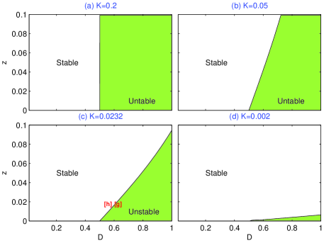
For K=0.2K0.2\mathrm{K}=0.2, 0.05, 0.02, and 0.002, the stable regions are shown in Fig. 19. For K<0.002K0.002\mathrm{K}<0.002, the whole region in Fig. 19 is almost stable. However, FSI still occurs for D>0.5𝐷0.5D>0.5 if z𝑧z is too small. From Fig. 19, the stability is z𝑧z dependent, even for small z<0.1𝑧0.1z<0.1.

Refer to caption
Figure 19: As K𝐾K decreases or z𝑧z increases, the stability region enlarges.

Example 3. (FSI with PM = 89superscript8989^{\circ}.) Continue from Example 1, but with large ωp=3.14×10⁹subscript𝜔𝑝3.14superscript109\omega_{p}=3.14\times 10^{9} rad/s (to make the type-II compensator act like a PI compensator), vs=5.6subscript𝑣𝑠5.6v_{s}=5.6 V, vc=0.574subscript𝑣𝑐0.574v_{c}=0.574 V, and Kc=460420subscript𝐾𝑐460420K_{c}=460420. Here, z=0.018𝑧0.018z=0.018, D=0.6𝐷0.6D=0.6 and K=0.0232K0.0232\mathrm{K}=0.0232. The converter is unstable (Fig. 20) although its average model has PM = 89superscript8989^{\circ} (Fig. 21). Independent sampled-data analysis shows an unstable pole at -1.02, and three stable poles at 0, 0.88, and 0.91.

Next, let vs=5.88subscript𝑣𝑠5.88v_{s}=5.88 V and vc=0.547subscript𝑣𝑐0.547v_{c}=0.547 V. Now, D=0.58𝐷0.58D=0.58. The converter is stable (Fig. 22). In Fig. 19(c), for K=0.02K0.02\mathrm{K}=0.02, draw a line at z=0.018𝑧0.018z=0.018, and the instability indeed occurs around D=0.6𝐷0.6D=0.6.     \Box

Refer to caption
Figure 20: The boost converter is unstable, vs=5.6subscript𝑣𝑠5.6v_{s}=5.6 V.
Refer to caption
Figure 21: The loop gain 𝒯(jω)𝒯𝑗𝜔\mathcal{T}(j\omega) has PM = 89superscript8989^{\circ}, vs=5.6subscript𝑣𝑠5.6v_{s}=5.6 V.
Refer to caption
Figure 22: The boost converter is stable, vs=5.88subscript𝑣𝑠5.88v_{s}=5.88 V.

The condition (21) can be also expressed in terms of KK\mathrm{K}:

K<1α0(D)/z+α1(D):=Kmax(D,z)K1subscript𝛼0𝐷𝑧subscript𝛼1𝐷assignsubscriptKmax𝐷𝑧\mathrm{K}<\frac{1}{\alpha_{0}(D)/z+\alpha_{1}(D)}:=\mathrm{K}_{\mathrm{max}}(D,z) (24)

if α0(D)/z+α1(D)subscript𝛼0𝐷𝑧subscript𝛼1𝐷\alpha_{0}(D)/z+\alpha_{1}(D) is positive.

For the boost converter, va=vosubscript𝑣asubscript𝑣𝑜v_{\mathrm{a}}=v_{o}, and (24) becomes

K=voRsKcVmLωs2<Kmax(D,z)Ksubscript𝑣𝑜subscript𝑅𝑠subscript𝐾𝑐subscript𝑉𝑚𝐿superscriptsubscript𝜔𝑠2subscriptKmax𝐷𝑧\mathrm{K}=\frac{v_{o}R_{s}K_{c}}{V_{m}L\omega_{s}^{2}}<\mathrm{K}_{\mathrm{max}}(D,z) (25)

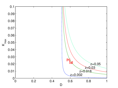
The plots of Kmax(D,z)subscriptKmax𝐷𝑧\mathrm{K}_{\mathrm{max}}(D,z) for different values of z𝑧z are shown in Fig. 23. For D<1/2𝐷12D<1/2, the converter is stable, agreed with Fig. 19. If z𝑧z is small, the converter is prone to be unstable for D>0.5𝐷0.5D>0.5, agreed with (23). As z𝑧z increases, Kmax(D,z)subscriptKmax𝐷𝑧\mathrm{K}_{\mathrm{max}}(D,z) increases and the stability region enlarges, also agreed with Fig. 19. The plots of Kmax(D,z)subscriptKmax𝐷𝑧\mathrm{K}_{\mathrm{max}}(D,z) also agree with Example 3. Draw a line at K=0.0232K0.0232\mathrm{K}=0.0232 in Fig. 23, the line intersects with Kmax(D,0.018)subscriptKmax𝐷0.018\mathrm{K}_{\mathrm{max}}(D,0.018) around D=0.6𝐷0.6D=0.6 indicating the onset of FSI at D=0.6𝐷0.6D=0.6 as discussed in Example 3.

In Fig. 23, given any value of z𝑧z, Kmax(D,z)subscriptKmax𝐷𝑧\mathrm{K}_{\mathrm{max}}(D,z) has a minimum at D=1𝐷1D=1. Then, a conservative (valid for any D𝐷D) stability condition is

K<Kmax(1,z)=zπ(1+πz)<zπKsubscriptKmax1𝑧𝑧𝜋1𝜋𝑧𝑧𝜋\mathrm{K}<\mathrm{K}_{\mathrm{max}}(1,z)=\frac{z}{\pi(1+\pi z)}<\frac{z}{\pi} (26)

As discussed above, ωcωsK/zsubscript𝜔𝑐subscript𝜔𝑠K𝑧\omega_{c}\approx\omega_{s}\mathrm{K}/z for z2Kmuch-less-thansuperscript𝑧2Kz^{2}\ll\mathrm{K}. Then, (26) is equivalent to ωc<ωs/πsubscript𝜔𝑐subscript𝜔𝑠𝜋\omega_{c}<\omega_{s}/\pi. This agrees with the tradition wisdom not to set a large ωcsubscript𝜔𝑐\omega_{c} to avoid FSI [5]. In Examples 1-3, FSI occurs with ωc>ωs/πsubscript𝜔𝑐subscript𝜔𝑠𝜋\omega_{c}>\omega_{s}/\pi.

Refer to caption
Figure 23: The plots of Kmax(D,z)subscriptKmax𝐷𝑧\mathrm{K}_{\mathrm{max}}(D,z) for the boost converter.

VI The Effect of the Voltage Feedback Loop Ripple

In the above analysis, vcsubscript𝑣𝑐v_{c} is assumed constant. In this section, the effect of vcsubscript𝑣𝑐v_{c} ripple generated from the voltage feedback loop is analyzed. Consider the PCMC buck converter, for example. Similar analysis can be applied to the ACMC case.

For PCMC, Gc(s)=1subscript𝐺𝑐𝑠1G_{c}(s)=1 and y=vcRsiL𝑦subscript𝑣𝑐subscript𝑅𝑠subscript𝑖𝐿y=v_{c}-R_{s}i_{L} which has two terms, for the voltage and current loops, respectively. Let (the ESR zero) ωr=1/RcCsubscript𝜔𝑟1subscript𝑅𝑐𝐶\omega_{r}=1/R_{c}C, r=ωr/ωs𝑟subscript𝜔𝑟subscript𝜔𝑠r=\omega_{r}/\omega_{s} and ρ=R/(R+Rc)𝜌𝑅𝑅subscript𝑅𝑐\rho=R/(R+R_{c}). Let G(s):=y(s)/vL(s)assign𝐺𝑠𝑦𝑠subscript𝑣𝐿𝑠G(s):=-y(s)/v_{L}(s). For the buck converter,

vo(s)iL(s)=R(Rc+1sC)=1+sωr1R+sCρρ(1+sωr)sC (at high frequency)subscript𝑣𝑜𝑠subscript𝑖𝐿𝑠conditional𝑅subscript𝑅𝑐1𝑠𝐶1𝑠subscript𝜔𝑟1𝑅𝑠𝐶𝜌𝜌1𝑠subscript𝜔𝑟𝑠𝐶 (at high frequency)\frac{v_{o}(s)}{i_{L}(s)}=R\parallel(R_{c}+\frac{1}{sC})=\frac{1+\frac{s}{\omega_{r}}}{\frac{1}{R}+\frac{sC}{\rho}}\approx\frac{\rho(1+\frac{s}{\omega_{r}})}{sC}\mbox{ (at high frequency)} (27)

Based on Fig. 4 and as shown in Fig. 24, the PCMC buck converter can be modeled as an SWG plus G(s)𝐺𝑠G(s), where

G(s)=(1+ρ(1+s/ωr)Gv(s)RsCs2)Gi(s)𝐺𝑠1𝜌1𝑠subscript𝜔𝑟subscript𝐺𝑣𝑠subscript𝑅𝑠𝐶superscript𝑠2subscript𝐺𝑖𝑠G(s)=(1+\frac{\rho(1+s/\omega_{r})G_{v}(s)}{R_{s}Cs^{2}})G_{i}(s) (28)

The loop gain is

𝒯(s)=vaG(s)Vm=vsG(s)VmvsRsVmLs+ρvs(1+s/ωr)Gv(s)VmLCs2𝒯𝑠subscript𝑣a𝐺𝑠subscript𝑉𝑚subscript𝑣𝑠𝐺𝑠subscript𝑉𝑚subscript𝑣𝑠subscript𝑅𝑠subscript𝑉𝑚𝐿𝑠𝜌subscript𝑣𝑠1𝑠subscript𝜔𝑟subscript𝐺𝑣𝑠subscript𝑉𝑚𝐿𝐶superscript𝑠2\mathcal{T}(s)=\frac{v_{\mathrm{a}}G(s)}{V_{m}}=\frac{v_{s}G(s)}{V_{m}}\approx\frac{v_{s}R_{s}}{V_{m}Ls}+\frac{\rho v_{s}(1+s/\omega_{r})G_{v}(s)}{V_{m}LCs^{2}} (29)
Refer to caption
Figure 24: A model for PCMC buck converter with closed voltage loop.

Three different voltage-loop compensators (with different Gv(s)subscript𝐺𝑣𝑠G_{v}(s)) are considered. The stability conditions have a universal form, vsRs(D0.5)/L<mamvsubscript𝑣𝑠subscript𝑅𝑠𝐷0.5𝐿subscript𝑚𝑎subscript𝑚𝑣v_{s}R_{s}(D-0.5)/L<m_{a}-m_{v}, even if different voltage-loop compensators are used, and those stability conditions are summarized in Table IV.

Table IV: Stability conditions for PCMC buck converter with open or closed voltage loop.
Universal stability condition: vsRs(D0.5)L<mamvsubscript𝑣𝑠subscript𝑅𝑠𝐷0.5𝐿subscript𝑚𝑎subscript𝑚𝑣\frac{v_{s}R_{s}(D-0.5)}{L}<m_{a}-m_{v}
      Voltage loop open: mv=0subscript𝑚𝑣0m_{v}=0
      Voltage loop closed:
         Proportional gain compensator, Gv(s)=kpsubscript𝐺𝑣𝑠subscript𝑘𝑝G_{v}(s)=k_{p}: mv=ρvskpTLCωs2[1rα0(D)+α1(D)]subscript𝑚𝑣𝜌subscript𝑣𝑠subscript𝑘𝑝𝑇𝐿𝐶superscriptsubscript𝜔𝑠2delimited-[]1𝑟subscript𝛼0𝐷subscript𝛼1𝐷m_{v}=\frac{\rho v_{s}k_{p}}{TLC\omega_{s}^{2}}[\frac{1}{r}\alpha_{0}(D)+\alpha_{1}(D)]
         Type-II compensator, Gv(s)=Kc(1+s/ωz)s(1+s/ωp)subscript𝐺𝑣𝑠subscript𝐾𝑐1𝑠subscript𝜔𝑧𝑠1𝑠subscript𝜔𝑝G_{v}(s)=\frac{K_{c}(1+s/\omega_{z})}{s(1+s/\omega_{p})}: mv=Kvωs2[α1(D)+(1p1r)(α(D,p)α0(D))]subscript𝑚𝑣subscript𝐾𝑣superscriptsubscript𝜔𝑠2delimited-[]subscript𝛼1𝐷1𝑝1𝑟𝛼𝐷𝑝subscript𝛼0𝐷m_{v}=\frac{K_{v}}{\omega_{s}^{2}}[\alpha_{1}(D)+(\frac{1}{p}-\frac{1}{r})(\alpha(D,p)-\alpha_{0}(D))]
         PI compensator, Gv(s)=Kc(1+s/ωz)ssubscript𝐺𝑣𝑠subscript𝐾𝑐1𝑠subscript𝜔𝑧𝑠G_{v}(s)=\frac{K_{c}(1+s/\omega_{z})}{s}: mv=Kvωs2[1rα0(D)+α1(D)]subscript𝑚𝑣subscript𝐾𝑣superscriptsubscript𝜔𝑠2delimited-[]1𝑟subscript𝛼0𝐷subscript𝛼1𝐷m_{v}=\frac{K_{v}}{\omega_{s}^{2}}[\frac{1}{r}\alpha_{0}(D)+\alpha_{1}(D)]
Note: p=ωp/ωs𝑝subscript𝜔𝑝subscript𝜔𝑠p=\omega_{p}/\omega_{s}, z=ωz/ωs𝑧subscript𝜔𝑧subscript𝜔𝑠z=\omega_{z}/\omega_{s}, r=ωr/ωs=1/RcCωs𝑟subscript𝜔𝑟subscript𝜔𝑠1subscript𝑅𝑐𝐶subscript𝜔𝑠r=\omega_{r}/\omega_{s}=1/R_{c}C\omega_{s}, ρ=R/(R+Rc)𝜌𝑅𝑅subscript𝑅𝑐\rho=R/(R+R_{c}), and Kv=ρvsKc/TLCωzsubscript𝐾𝑣𝜌subscript𝑣𝑠subscript𝐾𝑐𝑇𝐿𝐶subscript𝜔𝑧K_{v}=\rho v_{s}K_{c}/TLC\omega_{z}

VI-A Proportional Gain Compensator: Gv(s)=kpsubscript𝐺𝑣𝑠subscript𝑘𝑝G_{v}(s)=k_{p}

Let the voltage feedback be vc=kp(vrvo)subscript𝑣𝑐subscript𝑘𝑝subscript𝑣𝑟subscript𝑣𝑜v_{c}=k_{p}(v_{r}-v_{o}). From (29),

𝒯(s)=vsRsVmLs+ρvskp(1+s/ωr)VmLCs2𝒯𝑠subscript𝑣𝑠subscript𝑅𝑠subscript𝑉𝑚𝐿𝑠𝜌subscript𝑣𝑠subscript𝑘𝑝1𝑠subscript𝜔𝑟subscript𝑉𝑚𝐿𝐶superscript𝑠2\mathcal{T}(s)=\frac{v_{s}R_{s}}{V_{m}Ls}+\frac{\rho v_{s}k_{p}(1+s/\omega_{r})}{V_{m}LCs^{2}} (30)

From Table I, the stability condition is

vsRsα0(D)VmLωs+ρvskpVmLCωs2(1rα0(D)+α1(D))<1subscript𝑣𝑠subscript𝑅𝑠subscript𝛼0𝐷subscript𝑉𝑚𝐿subscript𝜔𝑠𝜌subscript𝑣𝑠subscript𝑘𝑝subscript𝑉𝑚𝐿𝐶superscriptsubscript𝜔𝑠21𝑟subscript𝛼0𝐷subscript𝛼1𝐷1\frac{v_{s}R_{s}\alpha_{0}(D)}{V_{m}L\omega_{s}}+\frac{\rho v_{s}k_{p}}{V_{m}LC\omega_{s}^{2}}(\frac{1}{r}\alpha_{0}(D)+\alpha_{1}(D))<1 (31)

or expressed in terms of the ramp slope

vsRs(D0.5)L<mamvsubscript𝑣𝑠subscript𝑅𝑠𝐷0.5𝐿subscript𝑚𝑎subscript𝑚𝑣\frac{v_{s}R_{s}(D-0.5)}{L}<m_{a}-m_{v} (32)

where, compared with (1), the (universal) stability condition (32) has an additional term

mv=ρvskpTLCωs2[1rα0(D)+α1(D)]subscript𝑚𝑣𝜌subscript𝑣𝑠subscript𝑘𝑝𝑇𝐿𝐶superscriptsubscript𝜔𝑠2delimited-[]1𝑟subscript𝛼0𝐷subscript𝛼1𝐷m_{v}=\frac{\rho v_{s}k_{p}}{TLC\omega_{s}^{2}}[\frac{1}{r}\alpha_{0}(D)+\alpha_{1}(D)] (33)

due to the effect of the voltage loop ripple. Note that α1(D)>0subscript𝛼1𝐷0\alpha_{1}(D)>0, but α0(D)<0subscript𝛼0𝐷0\alpha_{0}(D)<0 if D<0.5𝐷0.5D<0.5. Depending on whether mvsubscript𝑚𝑣m_{v} is positive or negative, the stability region shrinks or enlarges respectively by closing the voltage loop. It can be proved that for most practical buck converters, mv>0subscript𝑚𝑣0m_{v}>0.

The stability condition (31) can be also expressed in terms of kpsubscript𝑘𝑝k_{p},

kp<ωsCρ(VmLωsvsRsα0(D))1rα0(D)+α1(D)subscript𝑘𝑝subscript𝜔𝑠𝐶𝜌subscript𝑉𝑚𝐿subscript𝜔𝑠subscript𝑣𝑠subscript𝑅𝑠subscript𝛼0𝐷1𝑟subscript𝛼0𝐷subscript𝛼1𝐷k_{p}<\frac{\frac{\omega_{s}C}{\rho}(\frac{V_{m}L\omega_{s}}{v_{s}}-R_{s}\alpha_{0}(D))}{\frac{1}{r}\alpha_{0}(D)+\alpha_{1}(D)} (34)

Example 4. (Accurate prediction of critical gain kpsuperscriptsubscript𝑘𝑝k_{p}^{*}.) Consider a PCMC buck converter with the voltage loop closed from Example 4 of [1]. Simulation and independent sampled-data analysis show that FSI occurs at kp=237superscriptsubscript𝑘𝑝237k_{p}^{*}=237 (see Fig. 7 of [1]), which can be predicted by (34) exactly. In contrary, with kp=237subscript𝑘𝑝237k_{p}=237, the Ridley average model [10] shows that the converter is stable with an infinite gain margin and PM = 36.5superscript36.536.5^{\circ} [1]. \Box

VI-B Type-II Compensator: Gv(s)=Kc(1+s/ωz)/s(1+s/ωp)subscript𝐺𝑣𝑠subscript𝐾𝑐1𝑠subscript𝜔𝑧𝑠1𝑠subscript𝜔𝑝G_{v}(s)=K_{c}(1+s/\omega_{z})/s(1+s/\omega_{p})

Let the voltage feedback be vc=Gv(s)(vrvo)+vrsubscript𝑣𝑐subscript𝐺𝑣𝑠subscript𝑣𝑟subscript𝑣𝑜subscript𝑣𝑟v_{c}=G_{v}(s)(v_{r}-v_{o})+v_{r}, which has an additional offset vrsubscript𝑣𝑟v_{r} but it does not affect the loop gain. From (29), the loop gain is

𝒯(s)=vsRsVmLs+ρvsKc(1+s/ωr)(1+s/ωz)VmLCs3(1+s/ωp)𝒯𝑠subscript𝑣𝑠subscript𝑅𝑠subscript𝑉𝑚𝐿𝑠𝜌subscript𝑣𝑠subscript𝐾𝑐1𝑠subscript𝜔𝑟1𝑠subscript𝜔𝑧subscript𝑉𝑚𝐿𝐶superscript𝑠31𝑠subscript𝜔𝑝\mathcal{T}(s)=\frac{v_{s}R_{s}}{V_{m}Ls}+\frac{\rho v_{s}K_{c}(1+s/\omega_{r})(1+s/\omega_{z})}{V_{m}LCs^{3}(1+s/\omega_{p})} (35)

Generally ωzωsmuch-less-thansubscript𝜔𝑧subscript𝜔𝑠\omega_{z}\ll\omega_{s}. Let Kv=ρvsKc/TLCωzsubscript𝐾𝑣𝜌subscript𝑣𝑠subscript𝐾𝑐𝑇𝐿𝐶subscript𝜔𝑧K_{v}=\rho v_{s}K_{c}/TLC\omega_{z}. From Table I, the stability condition is also (32), where

mv=Kvωs2[α1(D)+(1p1r)(α(D,p)α0(D))]subscript𝑚𝑣subscript𝐾𝑣superscriptsubscript𝜔𝑠2delimited-[]subscript𝛼1𝐷1𝑝1𝑟𝛼𝐷𝑝subscript𝛼0𝐷m_{v}=\frac{K_{v}}{\omega_{s}^{2}}[\alpha_{1}(D)+(\frac{1}{p}-\frac{1}{r})(\alpha(D,p)-\alpha_{0}(D))] (36)

VI-C PI Compensator: Gv(s)=Kc(1/s+1/ωz)subscript𝐺𝑣𝑠subscript𝐾𝑐1𝑠1subscript𝜔𝑧G_{v}(s)=K_{c}(1/s+1/\omega_{z})

The PI compensator is a special case of the type-II compensator by setting ωpsubscript𝜔𝑝\omega_{p}\to\infty. Let the control voltage at the output of the voltage-loop compensator be vc=Gv(s)(vrvo)+vrsubscript𝑣𝑐subscript𝐺𝑣𝑠subscript𝑣𝑟subscript𝑣𝑜subscript𝑣𝑟v_{c}=G_{v}(s)(v_{r}-v_{o})+v_{r}. From (29), the loop gain is

𝒯(s)=vsRsVmLs+ρvsKc(1+s/ωr)(1+s/ωz)VmLCs3𝒯𝑠subscript𝑣𝑠subscript𝑅𝑠subscript𝑉𝑚𝐿𝑠𝜌subscript𝑣𝑠subscript𝐾𝑐1𝑠subscript𝜔𝑟1𝑠subscript𝜔𝑧subscript𝑉𝑚𝐿𝐶superscript𝑠3\mathcal{T}(s)=\frac{v_{s}R_{s}}{V_{m}Ls}+\frac{\rho v_{s}K_{c}(1+s/\omega_{r})(1+s/\omega_{z})}{V_{m}LCs^{3}} (37)

Generally ωzωsmuch-less-thansubscript𝜔𝑧subscript𝜔𝑠\omega_{z}\ll\omega_{s}. From Table I, the stability condition is also (32), where

mv=Kvωs2[1rα0(D)+α1(D)]subscript𝑚𝑣subscript𝐾𝑣superscriptsubscript𝜔𝑠2delimited-[]1𝑟subscript𝛼0𝐷subscript𝛼1𝐷m_{v}=\frac{K_{v}}{\omega_{s}^{2}}[\frac{1}{r}\alpha_{0}(D)+\alpha_{1}(D)] (38)

Note that (38) is for the PI compensator whereas (33) is for the proportional compensator. However, they are the same by setting kp=Kc/ωzsubscript𝑘𝑝subscript𝐾𝑐subscript𝜔𝑧k_{p}=K_{c}/\omega_{z}. The proportional compensator, though simple, can be used to predict FSI if a more complicated PI compensator is used.

VII Conclusion and Contributions

Based on [4, 5], a unified CMC model (Fig. 4) is proposed to predict FSI for different converters under PCMC or ACMC. Such a unified CMC model exists because any CMC converter is essentially a TWG with a linear feedback. Closed-form stability conditions are derived (see Table II) and verified by time-domain simulations (see Table III). The obtained results are consistent with (but broader than) the past research such as [3, 11]. The instability is found to be associated with large crossover frequency. A conservative condition to avoid FSI is ωc<ωs/πsubscript𝜔𝑐subscript𝜔𝑠𝜋\omega_{c}<\omega_{s}/\pi. The proposed model can be applied to converters with high-order compensators, such as type-II and PI compensators, for example.

The questions asked in the Introduction are answered:

  1. 1.

    FSI occurs in both the buck and the boost converters with the same parameters if they have the same vasubscript𝑣av_{\mathrm{a}}, as shown in Example 2.

  2. 2.

    The unified model can be applied to both PCMC and ACMC.

  3. 3.

    The same FSI condition expressed in terms of vasubscript𝑣av_{\mathrm{a}}, as shown in Table II, also applies to any CMC converter. For the buck converter, va=vs=vo/Dsubscript𝑣asubscript𝑣𝑠subscript𝑣𝑜𝐷v_{\mathrm{a}}=v_{s}=v_{o}/D. For the boost or buck-boost converter, va=vs/(1D)=vosubscript𝑣asubscript𝑣𝑠1𝐷subscript𝑣𝑜v_{\mathrm{a}}=v_{s}/(1-D)=v_{o}. For example, given a buck converter with vo=vaDsubscript𝑣𝑜subscript𝑣a𝐷v_{o}=v_{\mathrm{a}}D and a boost converter with vo=vasubscript𝑣𝑜subscript𝑣av_{o}=v_{\mathrm{a}}, if both of the converters have the same power stage parameters, then they have the same stability or instability.

  4. 4.

    Although different parameters have different effects, they can be consolidated into a few parameters: K𝐾K, D𝐷D, and p𝑝p. A single plot of Kmax(D,p)subscript𝐾max𝐷𝑝K_{\mathrm{max}}(D,p) can be used to predict FSI. The stability based on traditional average analysis is D𝐷D independent (Fig. 6), whereas the actual stability is D𝐷D dependent (Fig. 7).

To the author’s knowledge, the following contributions have not been reported:

  1. 1.

    The unified CMC model of Fig. 4, applicable to PCMC or ACMC buck, boost, and buck-boost converters.

  2. 2.

    The unified stability conditions in Table II.

  3. 3.

    The plots of Figs. 6, 7, 17-19, and 23, which are universal for any CMC converter, and they are not just for specific examples.

  4. 4.

    Using the plot of Kmax(D,p)subscript𝐾max𝐷𝑝K_{\mathrm{max}}(D,p) as a design tool to avoid FSI.

  5. 5.

    The effects of different parameters on the stability, such as K𝐾K, the compensator pole ωpsubscript𝜔𝑝\omega_{p} and zero ωzsubscript𝜔𝑧\omega_{z}, as shown in Figs. 7 and 19.

  6. 6.

    The conservative stability condition ωc<ωs/πsubscript𝜔𝑐subscript𝜔𝑠𝜋\omega_{c}<\omega_{s}/\pi for the CMC converter with a PI compensator (whereas the same condition for the CMC converter with the type-II compensator was reported in [5]).

  7. 7.

    The effect of the voltage loop ripple on FSI (see Table IV).

Although this paper focuses on CMC, the proposed analysis can be applied to other schemes (such as VMC and constant on-time control). As reported in [5], ACMC with type-II and PI compensators belong respectively to the cases 𝒞5subscript𝒞5\mathcal{C}_{5} and 𝒞7subscript𝒞7\mathcal{C}_{7}. The derived FSI conditions are also applicable to these cases. For example, a buck converter with V2superscriptV2\mathrm{V}^{2} control belongs to the case 𝒞7subscript𝒞7\mathcal{C}_{7} with K=vs/VmLCωs2Ksubscript𝑣𝑠subscript𝑉𝑚𝐿𝐶superscriptsubscript𝜔𝑠2\mathrm{K}=v_{s}/V_{m}LC\omega_{s}^{2} and ωz=1/RcCsubscript𝜔𝑧1subscript𝑅𝑐𝐶\omega_{z}=1/R_{c}C, and the stability condition is exactly (21). Also, a buck converter with a type-II, type-III, or phase-lead compensator belongs to the case 𝒞5subscript𝒞5\mathcal{C}_{5}, and the stability condition is exactly (10).

References

  • [1] C.-C. Fang. Sampled-data poles, zeros, and modeling for current mode control. Int. J. of Circuit Theory Appl., 41(2):111–127, Feb. 2013.
  • [2] Y. Chen, C. K. M. Tse, S. Qiu, L. Lindenmuller, and W. Schwarz. Coexisting fast-scale and slow-scale instability in current-mode controlled DC/DC converters: Analysis, simulation and experimental results. IEEE transactions on circuits and systems I, Regular papers, 55(10):3335–3348, Nov. 2008.
  • [3] T. Suntio, J. Lempinen, I. Gadoura, and K. Zenger. Dynamic effects of inductor current ripple in average current mode control. In Proc. IEEE PESC, pages 1259–1264, 2001.
  • [4] C.-C. Fang. Critical conditions for a class of switched linear systems based on harmonic balance: Applications to dc-dc converters. Nonlinear Dynamics, 70(3):1767–1789, Nov. 2012.
  • [5] C.-C. Fang. Closed-form critical conditions of subharmonic oscillations for buck converters. IEEE Trans. Circuits Syst. I, 60(7):1967–1974, Jul. 2013.
  • [6] C.-C. Fang. Closed-form critical conditions of instabilities for constant on-time controlled buck converters. IEEE Trans. Circuits Syst. I, 59(12):3090–3097, Dec. 2012.
  • [7] C.-C. Fang and R. Redl. Subharmonic stability limits for the buck converter with ripple-based constant on-time control and feedback filter. IEEE Trans. Power Electron., 29(4):2135–2142, Apr. 2014.
  • [8] C.-C. Fang and E. H. Abed. Saddle-node bifurcation and Neimark bifurcation in PWM DC-DC converters. In S. Banerjee and G. C. Verghese, editors, Nonlinear Phenomena in Power Electronics: Bifurcations, Chaos, Control, and Applications, pages 229–240. Wiley, New York, 2001.
  • [9] R. W. Erickson and D. Maksimovic. Fundamentals of Power Electronics. Springer, Berlin, Germany, second edition, 2001.
  • [10] R. B. Ridley. A new, continuous-time model for current-mode control. IEEE Trans. Power Electron., 6(2):271–280, 1991.
  • [11] J. Sun and R. M. Bass. Modeling and practical design issues for average current control. In Proc. IEEE APEC, pages 980–986, 1999.
  • [12] Y. Yan, F.C. Lee, and P. Mattavelli. Analysis and design of average current mode control using describing function-based equivalent circuit model. IEEE Trans. Power Electron., 28(10):4732–4741, Oct. 2013.
  • [13] L. H. Dixon. Average current-mode control of switching power supplies. Unitrode Power Supply Design Seminar Handbook, 1990.
  • [14] W. Tang, F. C. Lee, and R. B. Ridley. Small-signal modeling of average current-mode control. IEEE Trans. Power Electron., 8(2):112–119, Apr. 1993.
  • [15] C. Sun, B. Lehman, and R. Ciprian. Dynamic modeling and control in average current mode controlled PWM DC/DC converter. In Proc. IEEE PESC, pages 1152–1157, 1999.
  • [16] P Cooke. Modeling average current mode control. In Proc. IEEE APEC, pages 256–262, 2000.
  • [17] R. Li. Modeling average-current-mode-controlled multi-phase buck converters. In Proc. IEEE APEC, pages 3299–3305, Aug. 2008.
  • [18] R. Li, T. O’Brien, J. Lee, and J. Beecroft. A unified small signal analysis of DC-DC converters with average current mode control. In Proc. IEEE ECCE, pages 647–654, 2009.
  • [19] R. Li, T. O’Brien, J. Lee, and J. Beecroft. Effects of circuit and operating parameters on the small-signal dynamics of average-current-mode-controlled DC-DC converters. In IEEE 8th International Conference on Power Electronics and ECCE Asia, pages 60–67, 2011.
  • [20] F. Yu, F.C. Lee, and P. Mattavelli. A small signal model for average current mode control based on describing function approach. In Proc. IEEE ECCE, pages 405–412, 2011.
  • [21] C.-C. Fang. Asymmetric critical conditions for peak and valley current programmed converters at light loading. IEEE Transactions on Circuits and Systems-I: Regular Papers, 2013. accepted, available: http://dx.doi.org/10.1109/TCSI.2013.2284178.