Hole doped Dirac states in silicene by biaxial tensile strain
Abstract
The effects of biaxial tensile strain on the structure, electronic states, and mechanical properties of silicene are studied by ab-initio calculations. Our results show that up to 5% strain the Dirac cone remains essentially at the Fermi level, while higher strain induces hole doping because of weakening of the SiSi bonds. We demonstrate that the silicene lattice is stable up to 17% strain. It is noted that the buckling first decreases with the strain (up to 10%) and then increases again, which is accompanied by a band gap variation. We also calculate the Grüneisen parameter and demonstrate a strain dependence similar to that of graphene.
I Introduction
Silicene is a two dimensional buckled material which is closely related to graphene. It has been proposed as a potential candidate for overcoming the limitations of graphene because of stronger intrinsic spin orbit coupling (4 meV in silicene and meV in graphene cheng1 ). Silicene first has been reported to be stable by Takeda and Shiraishi takeda . Though C and Si belong to the same group of the periodic table, Si has a larger ionic radius, which promotes hybridization. Theoretical studies predict that free standing silicene has a stable two-dimensional buckled honeycomb structure ciraci ; olle , where the buckling is due to the mixture of and hybridizations. The magnitude of the buckling is 0.45 Å, which opens an electrically tunable band gap falko ; Ni , whereas the induced band gap due to the intrinsic spin orbit coupling amounts to 1.55 meV yao . The charge carriers behave like massless Dirac fermions in the and bands, which form Dirac cones at the Fermi level at the K and K′ points. The electronic properties of silicene and its derivatives have been studied in much detail by density functional theory calculations houssa ; Bechstedt ; kang ; Wang . In particular, it has been reported that the lattice is sensitive to the carrier concentration but still stable in a wide range of doping cheng .
Experimentally, growth of silicene and its derivatives has been reported for metallic substrates like Ag and ZrB2 padova ; vogt ; ozaki . Silicene on a ZrB2 thin film shows an asymmetric buckling due to strong interaction with the substrate, which increases the band gap. As in general accurate measurements of materials properties are problematic on substrates, it is desirable to achieve free standing silicene. However, this first requires the growth on appropriate substrates that make it possible to separate the silicene sheet. For the growth of silicene on any kind of substrate, the effect of strain is crucial to be understood. In this work, we focus on this topic using first-principles calculations. We apply strain up to 20% and calculate the corresponding band structure to evaluate the dependence of the induced doping on the strength of the biaxial tensile strain. Furthermore, we study the phonon spectrum to address the stability of the system and calculate the Grüneisen parameter.
II Computational details
We have carried out calculations using density functional theory in the generalized gradient approximation paolo . The van der Waals interaction grime ; jmc is taken into account in order to correctly describe the geometry. The calculations are performed with a plane wave cutoff energy of 816 eV. Moreover, a Monkhorst-Pack k-mesh is employed for optimizing the crystal structure and calculating the phonon spectrum, whereas a k-mesh is used for the density of states (DOS) in order to achieve higher resolution. The atomic positions are relaxed until an energy convergence of 10-9 eV and a force convergence of eV/Å are reached. We use an interlayer spacing of 16 Å to avoid artifacts of the periodic boundary conditions. The magnitude of the biaxial tensile strain is defined as , where and Å are the lattice parameters of the strained and unstrained silicene, respectively.
III Results and discussion
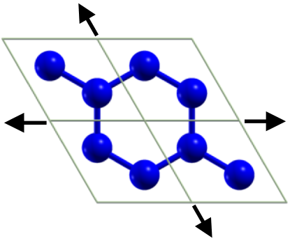
For graphene it has been demonstrated that 5 to 10% strain can be achieved without much efforts Andresa . The existing reports confirm this makes the system five times more reactive and H atoms are bound much stronger than in pristine graphene Andresa . Since a similar enhancement of H storage by strain can be expected for silicene, we study in the following the effect of strain on the electronic and mechanical properties. A top view of the crystal structure under consideration is shown in Fig. 1. For unstrained silicene we obtain a lattice parameter of Å and a buckling of 0.45 Å, consistent with previously reported data ciraci ; cheng . In a first step, we address the dependence of the force on the applied strain, see the results in Fig. 2. The force increases monotonically with the strain up to a strain of 17% and decreases thereafter, which indicates that silicene is stable up to 17% strain. The stability limit will be addressed in more detail via the phonon spectrum in the following section.

The band gap of 2 meV in unstrained silicene becomes smaller for increasing strain. Since strain weakens the internal electric field (by reducing the magnitude of the buckling) the spin orbit coupling and thus the induced band gap are reduced. The SiSi bond length is found to grow with the strain monotonically, which explains why the buckling decreases. Surprisingly, the buckling starts to increase again when the strain exceeds 10%. For example, unstrained silicene has a SiSi bond length of 2.28 Å and buckling of 0.46 Å. For 5% strain these values change to 2.37 Å and 0.32 Å, and for 17% strain to 2.47 Å and 0.30 Å. The variation of the SiSi bond length and buckling under strain are addressed in Fig. 3(a) and (b), respectively.
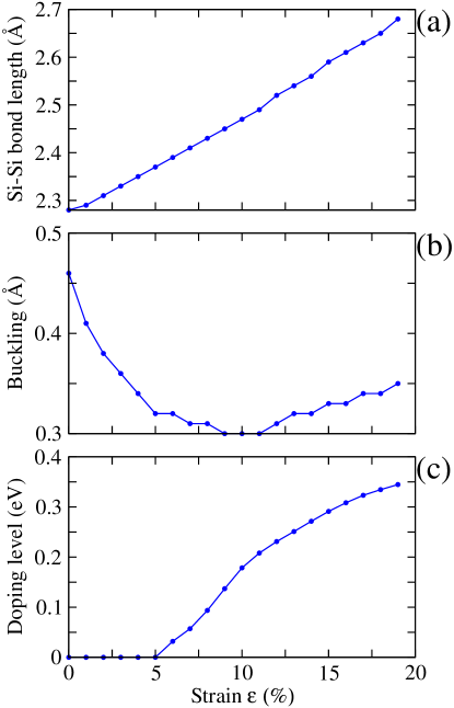
The variation of the doping level (defined as the shift of the Dirac cone with respect to the Fermi level) under strain is addressed in Fig. 3(c). It is well known that unstrained silicene is a semimetal, where the and orbitals give rise to and bands forming Dirac cones at the K and K′ points, see Fig. 4(a). The calculated band structure shows that the Dirac cone lies at the Fermi level upto a strain of 5% with a 2 meV band gap due to intrinsic spin orbit coupling. For higher strain the conduction band at the -point shifts towards the Fermi level, consistent with Ref. liu . At a strain of 7% it slightly crosses the Fermi level, which shifts the Dirac cone above the Fermi level by 0.06 eV, inducing hole doping, see Fig. 3(c). The doping is enhanced for increasing strain, since the conduction band minimum at the -point shifts further downwards and becomes more and more occupied (with an increasing DOS at the Fermi level). The main reason for hole doping in silicene under strain is this downshift and the consequent occupation of the band at the -point. It is a consequence of the weakening of the bonds due to the increasing SiSi bond length. Another ingredient is a reduction of the hybridization between the and orbitals, which in fact are occupied by 1.18 and 2.76 electrons in unstrained silicene, respectively, but by 1.33 and 2.63 electrons for 10% strain.
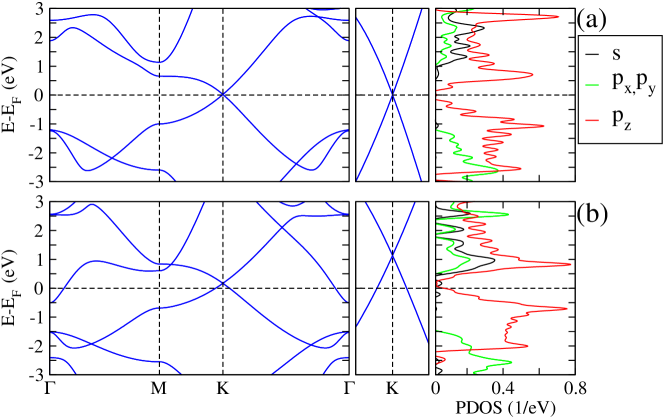
At 10% strain the Dirac point lies at 0.18 eV, see Fig. 4(b). We note that the and bands are due to the orbitals with minute contributions from the and orbitals, as expected, see the projected DOSs. For higher strain the conduction band minimum shifts further to lower energy and the Dirac cone accordingly to higher energy. It reaches 1.0 eV with the Dirac point at 0.34 eV for a strain of 20%. This behavior is different from graphene despite the quantitatively similar band structure, because the SiSi bonds are more flexible than the CC bonds. In contrast to silicene, graphene does not show significant changes in the electronic structure in the presence of strain, resulting a zero band gap semiconductor up to a huge strain of 30% son . As a result, doping cannot be achieved in graphene by strain.
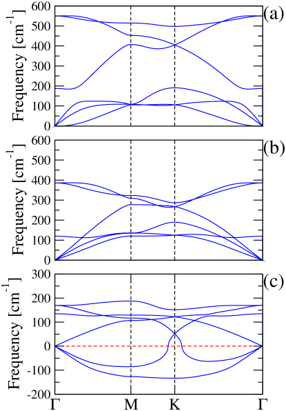
We now discuss the phonon spectrum of silicene without strain and under strain of 5%, 10%, 15%, 20%, and 25%. Without strain the optical phonon frequencies are found to be 33% smaller than in graphene cheng , which is understood by the smaller force constant and weaker SiSi bonds. In fact, the SiSi bond length of 2.28 Å is 37% larger than the CC bond length. In Fig. 5 we address the phonon band structure, where we focus on the highest branches at the -point (G mode) and the K-point (D mode). The calculated phonon frequencies at the and K-points are 550 cm-1 and 545 cm-1, respectively, which agree well with previous theoretical results ciraci ; cheng . A significant modification of the phonon frequencies is observed for strained silicene. For a strain of 5% the G and D mode frequencies amount to 460 cm-1 and 386 cm-1, respectively, reflecting the weakening of the SiSi bond under strain. Increase of the strain to 10% (17%) results in phonon frequencies of 372 cm-1 (296 cm-1) for the G mode and 272 cm-1 (187 cm-1) for the D mode. We still have positive frequencies along the -K direction and, hence, a stable lattice. An instability comes into the picture when the strain increases beyond 17%. At 20% strain we find a frequency of cm-1 and at 25% strain, see Fig. 5(c), the lattice is strongly instable. Importantly, no splitting of the G mode for increasing strain is observed in our calculations in contrast to graphene udo .
The Grüneisen parameter is an important quantity to describe strained materials as it measures the rate of phonon mode softening or hardening and, thus, determines the thermomechanical properties. The Grüneisen parameter for the G mode is given by
where is the difference in the frequency with and without strain and is the frequency of the G mode in unstrained silicene. A significant variation of the Grüneisen parameter between 1.64 and 1.42 for strain between 5 and 25 % is found, see Table I. These values are close to the experimental and theoretically values for graphene Mohiuddin ; ding ; udo ; Remi . While the experimentally reported Grüneisen parameters for graphene are not consistent due to substrate effects, there are no experimental data available for silicene for comparison. We find that the Grüneisen parameter first decreases with growing strain due to the reduced buckling of the two Si sublattices but increases again for higher strain as also the buckling increases. This behavior is fundamentally different from graphene, which is not subject to buckling. An experimental confirmation of our observations by Raman spectroscopy would be desirable.
| (%) | (cm-1) | |
|---|---|---|
| 5 | 460 | 1.64 |
| 10 | 372 | 1.62 |
| 15 | 296 | 1.54 |
| 20 | 246 | 1.34 |
| 25 | 160 | 1.42 |
IV Conclusion
In conclusion, we have used density functional theory to study the effect of biaxial tensile strain on the structure, electronic properties, and phonon modes of silicene. Our calculations demonstrate that up to 5% strain the Dirac cone remains essentially at the Fermi level but starts to shift to higher energy for higher strain. Therefore, strain can be used in silicene, in contrast to graphene, to induce hole doping. The different behavior of the two compounds, despite their close stuctural similarity, can be explained in terms of bonding and changes in the hybridizations. Strain results in a weakening of the SiSi bonds. As a consequence, an electronic band at the -point of the Brillouin zone shifts to lower energy and becomes partially occupied, which in turn leads to a depopulation of the Dirac cone. The buckling is found to decrease with increasing strain up to 10% but starts to increase again thereafter. Accordingly, the calculated Grüneisen parameter behaves differently than in graphene as the latter is not subject to buckling. Positive phonon frequencies up to a strain of 17% indicate lattices stability in this regime, whereas the lattice becomes instable at higher strain.
References
- (1) C.-C. Liu, H. Jiang, and Y. Yao, Phys. Rev. B 84, 195430 (2011).
- (2) K. Takeda and K. Shiraishi, Phys. Rev. B 50, 14916 (1994).
- (3) S. Cahangirov, M. Topsakal, E. Aktürk, H. Sahin, and S. Ciraci, Phys. Rev. Lett. 102, 236804 (2009).
- (4) S. Lebegue and O. Eriksson, Phys. Rev. B 79, 115409 (2009).
- (5) N. D. Drummond, V. Zólyomi, and V. I. Fal′ko, Phys. Rev. B 85, 075423 (2012).
- (6) Z. Ni, Q. Liu, K. Tang, J. Zheng, J. Zhou, R. Qin, Z. Gao, D. Yu, and J. Lu, Nano Lett. 12, 113 (2012).
- (7) C.-C. Liu, W. Feng, and Y. Yao, Phys. Rev. Lett. 107, 076802 (2011).
- (8) M. Houssa, E. Scalise, K. Sankaran, G. Pourtois, V. V. Afanasev, and A. Stesmans, Appl. Phys. Lett. 98, 223107 (2011).
- (9) F. Bechstedt, L. Matthes, P. Gori, and O. Pulci, Appl. Phys. Lett. 100, 261906 (2012).
- (10) J. Kang, F. Wu, and J. Li, Appl. Phys. Lett. 100, 233122 (2012).
- (11) Y. Ding and Y. Wang, Appl. Phys. Lett. 100, 083102 (2012).
- (12) Y. C. Cheng, Z. Y. Zhu, and U. Schwingenschlögl, EPL 95, 17005 (2011).
- (13) P. De Padova, C. Quaresima, C. Ottaviani, P. M. Sheverdyaeva, P. Moras, C. Carbone, D. Topwal, B. Olivieri, A. Kara, H. Oughaddou, B. Aufray, and G. Le Lay, Appl. Phys. Lett. 96, 261905 (2010).
- (14) P. Vogt, P. De, C. Quaresima, J. Avila, E. Frantzeskakis, M. C. Asensio, A. Resta, B. Ealet, and G. Le Lay, Phys. Rev. Lett. 108, 155501 (2012).
- (15) A. Fleurence, R. Friedlein, T. Ozaki, H. Kawai, Y. Wang, and Y. Yamada-Takamura, Phys. Rev. Lett. 108, 245501 (2012).
- (16) P. Giannozzi, S. Baroni, N. Bonini, M. Calandra, R. Car, C. Cavazzoni, D. Ceresoli, G. L. Chiarotti, M. Cococcioni, I. Dabo, A. Dal Corso, S. de Gironcoli, S. Fabris, G. Fratesi, R. Gebauer, U. Gerstmann, C. Gougoussis, A. Kokalj, M. Lazzeri, L. Martin-Samos, N. Marzari, F. Mauri, R. Mazzarello, S. Paolini, A. Pasquarello, L. Paulatto, C. Sbraccia, S. Scandolo, G. Sclauzero, A. P. Seitsonen, A. Smogunov, P. Umari, and R. M. Wentzcovitch, J. Phys. Condens. Matt. 21, 395502 (2009).
- (17) S. Grimme, J. Comput. Chem. 27, 1787 (2006).
- (18) T. P. Kaloni, Y. C. Cheng, and U. Schwingenschlögl, J. Mater. Chem. 22, 919 (2012).
- (19) P. L. de Andresa and J. A. Vergés, Appl. Phys. Lett. 93, 123531 (2008).
- (20) G. Liu, M. S. Wu, C. Y. Ouyang, and B. Xu, EPL 99, 17010 (2012).
- (21) S. M. Choi, S. H. Jhi, and Y. W. Son, Phys. Rev. B 81, 081407 (2010).
- (22) F. Ding, H. X. Ji, Y. H. Chen, A. Herklotz, K. Dorr, Y. F. Mei, A. Rastelli, and O. G. Schmidt, Nano Lett. 10, 3453 (2010).
- (23) Y. C. Cheng, Z. Y. Zhu, G. S. Huang, and U. Schwingenschlögl, Phys. Rev. B 83, 115449 (2011).
- (24) T. M. G. Mohiuddin, A. Lombardo, R. R. Nair, A. Bonetti, G. Savini, R. Jalil, N. Bonini, D. M. Basko, C. Galiotis, N. Marzari, K. S. Novoselov, A. K. Geim, and A. C. Ferrari, Phys. Rev. B 79, 205433 (2009).
- (25) C. Metzger, S. Remi, M. K. Liu, S. V. Kusminskiy, A. H. C. Neto, A. K. Swan, and B. B. Goldberg, Nano Lett. 10, 6 (2010).