Phase-sensitive transport at a normal metal-superconductor interface close to a Josephson junction
Abstract
Phase- and voltage bias-sensitive quasiparticle transport at a double interface is considered. The barriers range from tunnel to transparent, and the intermediate region has a width comparable to the superconducting coherence length. A phase difference is applied to the Josephson junction . The normal and Andreev reflections at the interface become -sensitive, and transport is governed by interferences within the narrow region, both in the normal and anomalous channels. The subgap conductance is separately (energy )- and (phase )- symmetric. Above the superconducting gap, the conductance is in general not symmetric even if is changed in , but the symmetry is restored by averaging Fermi oscillations. The Tomasch oscillations are amplified by the phase difference. The subgap conductance exhibits a resonant structure at the energy of the Andreev bound states (ABS) of the junction, providing a side-spectroscopy of such states. Depending on the relative transparencies of the junctions, the resonance can increase or reduce the conductance, and it can even vanish for , featuring total reflection of quasiparticles at by the ABS at .
pacs:
74.78.Na,74.45.+cI Introduction
Transport in hybrid set-ups involving interfaces between superconductors () and normal metals () is governed by Andreev reflection, where an incoming electron with energy is transformed into a hole with opposite energy in the metal ( is the chemical potential)Andreev ; SaintJames , and a Cooper pair enters the superconducting condensate. Conversely, an incoming hole may be reflected as an electron while a pair is taken from . Andreev scattering dominates subgap transport and it plays also a role at energies of order of a few times the superconducting gap. Using the Bogoliubov-De Gennes equations and writing the scattering equations for the electron and hole wavefunctions, De Gennes and Saint-James found subgap bound states in a thin metallic layer in contact with a superconductor SaintJames . Rowell and McMillan RowellMcMillan showed that conductance oscillations occur as well above the gap. TomaschTomasch discovered oscillations in the conductance above the gap in a structure, which were explained by McMillan and Anderson McMillanAnderson as an interference effect due to the wavevector mismatch between the electron and hole-like quasiparticle branches propagating in a narrow layer of thickness of the order of the superconducting coherence length .
Using the scattering approach, Blonder, Tinkham and Klapwijk BTK were able to bridge the gap between a Giaever tunneling barrier () and a perfectly transparent interface, where the conductance is doubled below the gap, with respect to the normal case. The scattering approach had been used previously for a double interface by Kulik Kulik in the transparent case, then in many subsequent works, to obtain a complete description of a clean Josephson junction. It is characterized by the formation of Andreev bound states (ABS), as resonant states formed by multiple electron-electron and electron-hole scattering at each interface. The phase dispersion of the ABS is responsible for the Josephson current flowing through the junction. Recently, a tunnel spectroscopy of the ABS was performed by attaching a third contact to the normal bridge of a long junction Pillet . A microwave spectroscopy of the ABS was recently obtained in an atomic point contact Saclay ; Bretheau and a diffusive metallic junction Bouchiat .
These effects have been probed experimentally in two-terminal transport geometries. In addition, tunnel spectroscopy of the ABS involves a third reservoir, weakly coupled directly to the junction Pillet ; Giazotto . Coupling a Josephson junction to a normal wire has also been proposed and achieved SSNN . Recently, new three-terminal hybrid configurations exploiting the mesoscopic size of Cooper pairs have been explored. For instance, consider a geometry where two normal leads (or quantum dots) are connected by a narrow superconducting region, of size comparable to the superconducting coherence length . Then, a mechanism denoted as crossed (or nonlocal) Andreev reflection allows a hole incoming on one side to be transmitted as an electron on the other, effectively splitting a Cooper pair from the superconductor, into a pair of correlated quasiparticles CAR . Those carry opposite energies and spins (for an s-wave superconductor), and this mechanism has been proposed as a source of entangled fermions in the solid state Recher . A three-terminal all-superconducting set-up, called as a Josephson bijunction, has been more recently considered Cuevas2007 ; Houzet2010 ; Freyn2011 ; Jonckheere2013 ; Coupiac2011 ; Pfeffer2013 . It was shown that the two independent phase degree of freedom (or voltages) leads to novel coherent multipair dc channels, which coexist with dissipative quasiparticle transport for some combinations of applied voltages.
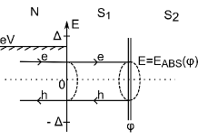
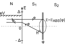
In what follows, we investigate a hybrid structure where Andreev reflection interferes with Josephson transport at a neighbouring junction. It is controlled by one voltage and one phase, as independent variables. More specifically, we explore the properties of a hybrid bijunction , made of a interface, in close proximity with a Josephson junction . The transparencies of the two interfaces are arbitrary. The Josephson junction is biased with a phase difference . A possible experimental device is sketched on Fig.1. Alternatively, the phase difference can also be imposed by an applied current, in a three-terminal geometry, but accessing only the range .
To modelize such a structure, we consider a one-dimensional scattering model with two interfaces in series. As a consequence, the currents at the interfaces et are not necessarily equal. The quasiparticle current in N is converted into a Cooper pair current flowing, partly through the junction, the other part in the upper branch of the loop. In spite of the presence of interferences in this set-up, the geometry is very different from the usual Andreev interferometer containing two interfaces in parallel Andreevinterferometer . The conductance through the interface is calculated within the scattering approach. The phase difference between and , as a new control variable, brings quantitative and qualitative changes as compared to previous calculations including scattering within a single superconductor Bagwell . Resonant tunneling in a double barrier geometry was also investigated in Ref. Morpurgo, , focusing on the case of ideal interfaces. Conversely, we consider here an asymmetric structure where, in addition, the transparencies of the and junctions are arbitrary.
In this work, we calculate the conductance as a function of the voltage energy and the phase . This conductance is the derivative of the current through the interface with respect to the voltage on , the two superconducting regions and being grounded but phase-biased. A first result is that the energy and phase symmetries of the Andreev reflection probability are broken above the gap. Second, the Tomasch conductance oscillations become phase-sensitive and they are amplified. Third, the subgap conductance displays a resonant behavior close to the ABS state energies, yielding a novel ABS spectroscopy tool. Changing the interface parameters, this resonance crosses-over between a conductance maximum, featuring “transmission” tunneling spectroscopy, and a conductance minimum, featuring “reflection” spectroscopy. The first situation is encountered when the barrier is a tunnel barrier or at least less transparent than the one, while the second case, less conventional, corresponds to the converse where the barrier is more transparent than the one. The perfect cancellation of the conductance at at the ABS energy is a striking property, due to the suppression of the Andreev reflection by interference between the two interfaces.
Sec. II presents the model and an analytical solution for the simple limiting case of perfectly transparent interfaces. Sec. III focuses on the conductance above the gap. Sec. IV details the subgap conductance. Sec. V provides a general discussion.
II The model
II.1 Matching equations
A double interface is considered. For sake of simplicity, we assume that the Fermi energy and velocity are the same in all materials, and that the superconductors and have the same gaps (this corresponds to the scheme of Fig.1 where the superconducting loop is made of the same material). The barrier transparencies are defined as where are the amplitudes of delta-function barriers at the interfaces BTK . The phases are and . This one-dimensional model can be extended to more realistic interfaces, as discussed at the end of the paper. In the case of and having different electronic parameters, this is known to quantitatively modify the scattering equations, making the barrier less transparent. For instance, for a transparent interface, a wavevector mismatch is exactly equivalent to an effective barrier . The main conclusions of the work will thus not be qualitatively modified, and the present calculation can be easily extended to take into account a parameter mismatch. Following BTK BTK , a right-moving electron wavefunction in is incoming onto the interface. The quasiparticle wavefunctions in , and can then be written as
| (1) |
where , , , , , , , are amplitude probabilities: (resp. ) for Andreev (resp. normal) reflection to the left in , (resp. ) for electron-like (resp. hole-like) right-moving waves in , (resp. ) for electron-like (resp. hole-like) left-moving waves in , (resp. ) for electron-like (resp. hole-like) right-moving waves in (see Fig. 2). Here
| (2) |
with the relation and .
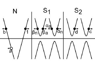
As shown below, generically, here for a nonzero phase difference, the conductance is not symmetric in energy, e.g. the standard BTK relation for a single interface does not hold any longer in the considered set-up (see Table 1). It is therefore convenient to use Eq. (1) for , and to use instead for similar equations for an incoming hole with amplitudes etc… (see Fig. 3):
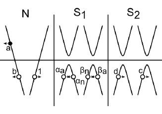
| (3) |
Denoting as and the normally reflected probability and the Andreev reflected one (from a hole at energy to an electron at energy ), the quasiparticle current entering is given byBTK
| (4) |
where is the Fermi density of states in , the Fermi velocity and the junction area. is the equilibrium Fermi distribution. Thus the differential conductance is at zero temperature ( is the number of channels):
| (5) |
| Figure No | ||||
|---|---|---|---|---|
| or , | 4,5,7a | yes | yes | yes |
| or , | 4,5,7a | no | no | yes |
| and , | 6,7b | yes | yes | yes |
| and , | 6,7b | no | no | no |
The reference chemical potential is the one of . The solutions to Eqs. (1) and (3) are obtained by matching the wavefunction and its derivative at the interface in a standard procedure BTK . Following the Andreev approximation, the wavevectors as factors in the derivatives of the wavefunctions, but their full expressions are kept in the exponentials. A complete analytical solution can be obtained, but it is too lengthy to be reported here. Yet it can be used to check certain symmetry properties. For instance, the time-reversal symmetry is obeyed, manifesting here in the relation and . The sign change in the phase reflects that of the (orbital) magnetic field, and time symmetry also inverts momenta as apparent from the matching equations (1) and (3).
II.2 Analytical results in limiting cases
An analytical solution can be written for perfectly transparent contacts (). Such perfect contacts are an ideal limiting regime, that can be approached with quantum point contacts. For an incoming electron, the solution reads
| (6) | |||
| (7) |
and , where .
For energies larger than , is in general a complex number whereas for energies lower than , is always a real number . One verifies easily that for , a result thus insensitive to (see Fig. 4).
The situation is different for . The condition expresses the occurrence of constructive interferences between the two waves and within the width of . This leads to the BTK-like scattering amplitudes .
The condition reads
| (8) |
which indicates the maxima in the Tomasch oscillations.
Another interesting limiting case is that of high energies , with and . Then,
| (9) |
thus
| (10) |
Eq. (10) leads to proportionnal to for all . Thus, the conductance at is larger than the conductance at if . (see Fig. 4). This trend helps to understand the more general results presented later on.
On the other hand in the case of an incoming hole, one finds that
| (11) | |||
| (12) |
and . Then the question of changing sign of both arises. Indeed if one changes , and in Eqs. (6) and (7), one finds that the moduli of and in Eqs. (6) and (7), and of and in Eqs. (11) and (12) are respectively equal. There is no symmetry under inversion of or separately, but there is symmetry under simultaneous inversion of (see Fig. 4). As shown below, this does not hold any longer if and are both nonzero.
 |
 |
| a) | b) |
 |
 |
| c) | d) |
III Conductance above the gap
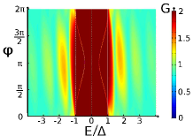
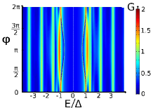
Let us first discuss how the excess conductance due to Andreev reflections above the gap is modified by the phase difference . As shown above for perfectly transparent interfaces, the conductance at can be much larger than at . This behavior holds also for arbitrary , , as seen from the forthcoming discussion.
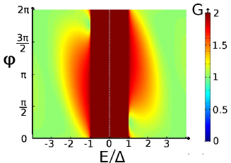
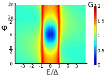
First, taking either (, ) or (, ), Fig. 5 shows maps of the conductance as a function of energy and phase for several values of . Symmetry of the conductance between () and () is obtained in each case. Second, the distinguishing features of Tomasch interferences appear as fringes in Fig. 5. Their enhancement by a phase difference is visible and culminates at . Moreover, the conductance just above the gap is markedly modified by the phase : the gap edge anomaly is shifted to higher energies, with a maximum for , instead of a gap edge anomaly exactly at for a single NS interfaceBTK .
 |
 |
| a) | b) |
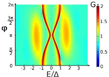
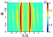
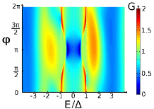
If none of the barriers is perfectly transparent, e.g. generically and then no symmetry exists in energy and phase (see Figs. 6a, 7b). As mentioned above, this is not contradictory with the existence of a time inversion symmetry, but should be traced back to the combination of several relevant phase shifts : those at the interfaces, related to and , the wavevector phase shifts and the -dependent Andreev phase shifts at each of the two interfaces. Careful examination of the analytical solution of Eqs. (1) and (3) shows that the probabilities and are formed by two kinds of terms. Those involving the phase shift , happen to be even in and , and they are symmetric in . When and are both different, new terms containing also appear, which are no more even in and , and lead to breaking of the symmetry, e.g. . This differences oscillates as , and is expected to disappear with disorder, interface roughness or simply two-dimensional character of the interfaces.
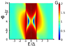
On the other hand, when and are comparable, the behavior for features a Fabry-Pérot-like cavity, with quasi-periodic fringes extending at high energy (see Fig. 6a). Since in a real experiment with extended interfaces, the length is expected to fluctuate at the scale of the Fermi wavelength , those fringes are expected to partially average out, as seen on Fig. 6b.
IV Subgap conductance
IV.1 Small case
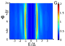
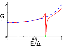
The subgap conductance exhibits very interesting structures. First, if , and with a transparent interface, most of the subgap conductance is suppressed for phases close to , as for instance for (see Fig. 7a). This is an interference phenomenon, culminating at where the amplitudes of Andreev reflections at and are just opposite to each other. For small , this destructive interference holds in most of the subgap domain. For (see Fig. 5a) or larger, it concentrates on a narrow energy interval, a phenomenon that we discuss below.
 |
 |
| a) | b) |
If on the other hand if the first interface is less transparent, for instance , the behavior for displays a pinching of the Andreev resonance anomaly (see Fig. 5c), shifted at energies lower than the gap, with a minimum at , going to zero energy if is large compared to .
IV.2 Large case
IV.2.1 Numerical results
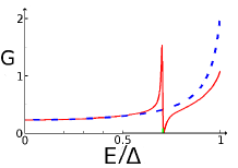
For small , together with the shift of the Andreev maximum towards above the gap (see Fig. 5b), there appears a conductance dip inside the subgap region with high conductance. Conversely, in the opposite case where (see Fig. 5d), the anomaly follows a similar energy and phase variation but is dominated by a conductance excess.
IV.2.2 Analytical results for the conductance maxima and minima
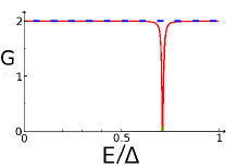
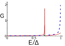
Those trends are better understood by plotting the subgap conductance as a function of energy, for instance at and . Fixing and varying from to shows a drastic evolution (see Fig. 8). For , a sharp conductance minimum appears, reaching zero. As increases, a conductance maximum develops in addition, and it dominates the anomaly for . The conductance at the minimum is equal to zero only if . For other values of the phase, the conductance minimum does not reach zero.
 |
 |
| a) | b) |
 |
 |
| c) | d) |
An analytical insight of both the minimum and maximum of the conductance can be obtained. Let us first set . Then one looks for zeros of the normal reflection coefficient , meaning that Andreev reflection is total at the interface, in spite of . One gets an energy-phase condition (here ):
| (13) |
If is large compare to , Eq.(13) simplifies into , and one obtains
| (14) |
corresponding to the ABS energy for a transparent single channel contact (or many degenerate channels for a planar interface). If the interface between and is not perfectly transparent and if is large compared to , the normal metal electrode can act like a side tunneling probe, with a conductance maximum at the the energy of the ABS localized at the interface (see Figs. 5d and 8d). Otherwise, if the barrier at the interface perturbs more strongly the reflections involved in the ABS, and an energy gap opens between negative and positive-energy ABS, as observed in Fig 5c, together with substantial broadening.
An unexpected behavior is encountered if the barrier is more transparent than the Josephson barrier . As shown in Figs 8a, b), the spectroscopic signature of the ABS is a conductance minimum. Again, an analytical solution can be obtained for , looking for maxima (instead of zeros) in the reflection coefficient . This yields
| (15) |
where . Solving this equation, one finds
| (16) |
where is the Josephson junction transparency. Eq. (16) is the ABS energy for a single channel with barrier .
V Discussion and conclusion
V.1 Discussion of the results
The above results show that Andreev scattering at a interface displays a rich behavior if the width of is comparable to the coherence length and a phase difference can be applied at the junction . Above the gap, the interferences between quasiparticle modes propagating within become phase-sensitive, which enhances the Tomasch oscillations with a maximum at .
An interference occurs between the Andreev scattering amplitudes at the two interfaces for subgap voltage. At large , a sharp resonance appears at the energy of the ABS. To be observable, the transparency of the Josephson junction should be large enough, so that the ABS extends inside the superconducting gap. The structure of this resonance displays a maximum and a minimum of conductance, separated by a small energy difference (see Fig. 8). The relative weight of the maximum and minimum depends on the respective transparencies of the two interfaces. When , it is dominated by an enhanced transmission, in a way similar to tunnel spectroscopy. The normal reflection amplitude has a minimum and the Andreev reflection amplitude a maximum. Conversely, when , a destructive interference occurs in the Andreev channel. For , this interference completely cancels Andreev reflection, thus the conductance becomes zero, and this is even true for any value of , and , except for very small values (see Fig. 8). This spectacular result means that the superconductor becomes opaque to quasiparticles coming from the normal metal. Symmetrically, quasiparticles involved in ABS at the Josephson junction are completely reflected at the interface. For phases different from , reflection is partial, but a sharp minimum occurs and this is enough to detect the ABS. Let us stress that the larger , the sharper the resonance, which exists even for . This is is due to the divergence of the effective scattering length at the resonance, in a way similar to the usual Andreev resonance at the gap edge in the case of a single NS interface.
It is possible to interpret the conductance maximum and minimum by diagrams in the corresponding limiting cases. Fig. 9a show a constructive interference between Andreev reflections at and , where multiple Andreev reflections builds the ABS. On the other hand, Fig. 9b shows a constructive interference between normal reflections at and multiple Andreev reflections at . The perfect reflection at implies the formation of a resonant state within the superconductor, which involves a Cooper pair crossing and a crossed Andreev reflection ( line in Fig. 10). This three-body process can also be viewed as an exchange process between a single quasiparticle and one member of a Cooper pair, accompanied by a pair crossing the junction.
 |
 |
| a) | b) |
The situation , where the spectroscopic signature of the Andreev states is a conductance minimum, is especially interesting. Then the quasiparticle current flowing at the interface can be larger than the critical current at the junction. The scattering approach does not ensure conservation of the quasiparticle current, since quasiparticles are converted into Cooper pairs. The excess current in compared to should flow in the upper branch of the set-up (Fig. 1).
V.2 Multichannel or two-dimensional contacts, and effects of disorder
The above analysis considers the most simplified one-dimensional model, at zero temperature. It can describe parallel interfaces with the same number of (nondispersive) channels. Or in the spirit of BTK BTK , it can be taken as a phenomenological approach to a few channel point contact probed by a tunneling tip in its close vicinity (or a Sharvin contact). Yet, the general trends of the considered model should be revealed in a more realistic set-up. First, at nonzero temperature, Fermi broadening of the electronic distribution in will smear the conductance anomalies reported in this work. Second, a multichannel generalization of the scattering method is possible. If the junction has many dispersive or diffusive channels, it defines ABS extending in energy above some minigap , and one expects that the anomaly of the conductance will reveal the phase dependence of this minigap (this also holds if the junction is a diffusive junction). Depending on temperature and ABS level spacing, peaks or dips in the conductance can be resolved, or on the contrary merge into a shoulder (or trough) extending between and the gap .
Disorder such as point disorder in or interface roughness is expected to have very different effects, depending on whether the voltage is larger or smaller than the gap. In the former case, disorder in the superconductor can easily blur the Tomasch oscillations, unless the elastic mean-free path is larger than (clean superconductor). In addition, it is expected to restore the symmetry . In the subgap regime, on the contrary, the spectroscopic signatures of the ABS are pinned to the ABS energy and should be quite robust as suggested by averaging out fluctuations in in the present calculation. Last but not least, disorder in the normal metal can amplify the Andreev reflection at low energy and give rise to subgap anomalies, by ”reflectionless tunneling”. To treat all these effects and perform more realistic calculations, in terms of geometry and disorder, one requires more advanced methods using nonequilibrium Green’s functions. Such methods also allow to calculate the dependence with of the Josephson current, not addressed in this work. In the case of large transparency and many channels at the interface, one should include self-consistency of the gap, and also possible nonequilibrium effects.
In the case of the three-terminal geometry with different superconductors and , those might have different gaps . One expects that the structure of the ABS below the smallest gap is revealed in , and that a more complex behaviour is obtained between and .
On the other hand, on the more classic tunnel spectroscopy case , where the probe little perturbs the junction, the present configuration is advantageous in terms of spectroscopy of the ABS. This work suggests a “side-spectroscopy” by letting a scanning tunneling tip or narrow contact come at a distance of order from the junction (see Fig. 1).
In conclusion, we have revealed the rich behavior a double interface, when the independent control parameters are a voltage bias and a superconducting phase difference, respectively applied to the two interfaces. Phase-sensitive Tomasch oscillations, together with various spectroscopic probes of the ABS, are predictions that could be tested in a realistic device.
The authors acknowledge support from the Agence Nationale de la Recherche (contract Nanoquartets 12 BS10 007 01). The authors also thank H. Courtois, C. Winkelmann and B. Douçot for fruitful discussions.
References
- (1) A. F. Andreev, Zh. Eksp. Teor. Fiz. 46, 1823 (1964) [Sov. Phys. JETP 19, 1228 (1964)].
- (2) P. G. de Gennes and D. Saint-James, Phys. Lett. 4, 151 (1963).
- (3) J. M. Rowell and W. L. McMillan, Phys. Rev. Lett. 16, 453 (1966); J. M. Rowell, Phys. Rev. Lett. 30, 167 (1973).
- (4) W. J. Tomasch, Phys. Rev. Lett. 15, 672 (1965); W. J. Tomasch, Phys. Rev. Lett. 16, 16 (1966).
- (5) W. L. McMillan and P. W. Anderson, Phys. Rev. Lett. 16, 85 (1966).
- (6) G. E. Blonder, M. Tinkham, and T. M. Klapwijk, Phys. Rev. B 25, 4515 (1982).
- (7) I. O. Kulik, Zh. Eksp. Teor. Fiz. 57, 1745 (1969) [Sov. Phys. JETP 30, 944 (1970)].
- (8) J-D. Pillet, C. Quay, P. Morfin, C. Bena, A. Levy Yeyati, and P. Joyez, Nature Phys. 6, 965 (2010).
- (9) M. Meschke, J. T. Peltonen, J. P. Pekola, and F. Giazotto, Phys. Rev. B 84, 214514 (2011).
- (10) E. Scheer, P. Joyez, D. Estève, C. Urbina and M. H. Devoret, Phys. Rev. Lett. 78, 3535 (1997).
- (11) L. Bretheau, Ç. Ö. Girit, H. Pothier, D. Estève and C. Urbina, Nature 499, 312 (2013).
- (12) B. Dassonneville, M. Ferrier, S. Guéron, and H. Bouchiat, Phys. Rev. Lett. 110, 217001 (2013).
- (13) C. J. Lambert and A. Martin, J. Phys. C 6, L221 (1994); A. F. Morpurgo, B. J. van Wees and T. M. Klapwijk, and G. Borghs, Phys. Rev. Lett. 79, 4010 (1997); A. F. Morpurgo, T. M. Klapwijk and B. J. van Wees, Appl. Phys. Lett. 72, 966 (1998); H. Tolga Ilhan and P. F. Bagwell, Appl. Phys. 84, 6758 (1998).
- (14) J. M. Byers and M. E. Flatté, Phys. Rev. Lett. 74, 306 (1995); T. Martin, Phys. Lett. A 220, 137 (1996); G. Deutscher and D. Feinberg, Appl. Phys. Lett. 76, 487 (2000); D. Beckmann, H. B. Weber, and H. v. Löhneysen, Phys. Rev. Lett. 93, 197003 (2004); S. Russo, M. Kroug, T. M. Klapwijk, and A. F. Morpurgo, Phys. Rev. Lett. 95, 027002 (2005); P. Cadden-Zimansky, and V. Chandrasekhar, Phys. Rev. Lett. 97, 237003 (2006).
- (15) P. Recher, E. V. Sukhorukov, and D. Loss, Phys. Rev. B 63 , 165314 (2001).
- (16) J. C. Cuevas and H. Pothier, Phys. Rev. B 75, 174513 (2007).
- (17) M. Houzet and P. Samuelsson, Phys. Rev. B82, 060517 (2010).
- (18) A. Freyn, B. Douçot, D. Feinberg, R. Mélin, Phys. Rev. Lett. 106, 257005 (2011).
- (19) T. Jonckheere, J. Rech, T. Martin, B. Douçot, D. Feinberg, and R. Mélin, Phys. Rev. B 87, 214501 (2013).
- (20) B. Kaviraj, O. Coupiac, H. Courtois, and F. Lefloch, Phys. Rev. Lett. 107, 077005 (2011)
- (21) A. H. Pfeffer, J. E. Duvauchelle, H. Courtois, R. Mélin, D. Feinberg, and F. Lefloch, arXiv:1307.4862 (2013).
- (22) P. G. N. de Vegvar, T. A. Fulton, W. H. Mallison, and R. E. Miller, Phys. Rev. Lett. 73 1416 (1994); H. Pothier, S. Guéron, D. Estève, and M. H. Devoret, Phys. Rev. Lett. 73 2488 (1994).
- (23) P. F. Bagwell, Phys. Rev. B 46, 12573 (1992).
- (24) A. F. Morpurgo and F. Beltram, Phys. Rev. B 50, 1325 (1994).
- (25) S. Chaudhuri and P. F. Bagwell, Phys. Rev. B 51, 16936 (1995).