Experimental Proof of Universal Conductance Fluctuation in Quasi-1D Epitaxial Bi2Se3 Wires
Abstract
We report on conductance fluctuation in quasi-one-dimensional wires made of epitaxial Bi2Se3 thin film. We found that this type of fluctuation decreases as the wire length becomes longer and that the amplitude of the fluctuation is well scaled to the coherence, thermal diffusion, and wire lengths, as predicted by conventional universal conductance fluctuation (UCF) theory. Additionally, the amplitude of the fluctuation can be understood to be equivalent to the UCF amplitude of a system with strong spin-orbit interaction and no time-reversal symmetry. These results indicate that the conductance fluctuation in Bi2Se3 wires is explainable through UCF theory. This work is the first to verify the scaling relationship of UCF in a system with strong spin-orbit interaction.
I Introduction
Bi2Se3 is a well-known and long-studied material with excellent thermoelectric properties that consists structurally of a layered semiconductor with a narrow band gap and strong spin-orbit interaction. Bi2Se3 has recently seen a resurgence in interest as a typical material of three dimensional topological insulators (3DTIs), which have spin-polarized Dirac electrons on the surface and a bulk band gap Hasan and Kane (2010). Previously, 3DTIs have been theoretically predicted Kane and Mele (2005); Fu and Kane (2007) and experimentally produced Hsieh et al. (2008). Because its surface state is protected against time-reversal-invariant perturbation, it is anticipated that 3DTIs will be used in spintronics Yazyev et al. (2010) and quantum computing Akhmerov et al. (2009). In order to facilitate such future applications and better understand the properties of surface Dirac electrons as well as electrons with strong spin-orbit interactions in the layered semiconductor, it is important to analyze the quantum transport properties of the material.
Several groups have already reported theoretical or experimental results relevant to characteristics of quantum transport phenomena, such as the weak antilocalization (WAL) effect, in intrinsic or doped Bi2Se3 Checkelsky et al. (2009, 2011); Qu et al. (2011); Chen et al. (2011); Wang et al. (2011); Steinberg et al. (2011); Chen et al. (2010); Liu et al. (2011); Kim et al. (2011); Onose et al. (2011); Taskin et al. (2012); Bao et al. (2012); Lu and Shen (2011). However, there is little available information on conductance fluctuation in Bi2Se3 Checkelsky et al. (2009, 2011); Matsuo et al. (2012); Li et al. (2012), even though universal conductance fluctuation (UCF) Stone (1985); Lee and Stone (1985); Altshuler (1985); Lee et al. (1987); Akkermans and Montambaux (2007) is an important phenomenon in quantum transport that has attracted a good deal of theoretical interest Rossi et al. (2012); Adroguer et al. (2012). Additionally, as the pioneering work on conductance fluctuation in Bi2Se3 Checkelsky et al. (2009) reported that neither the amplitude nor the correlation function behavior of conductance fluctuation can be explained by UCF, its origin in Bi2Se3 remains controversial. In addition, there have been no quantitative reports on the amplitude scaling relationship of UCF in systems such as Bi2Se3 with strong spin-orbit interaction. A quantitative study of conductance fluctuation in Bi2Se3 is therefore essential to understanding the fundamental coherence physics of this material.
Previously, we reported on the temperature dependence of the amplitude of fluctuation in Bi2Se3 and compared the coherence length derived from the WAL effect with that from UCF Matsuo et al. (2012). While these results confirmed that UCF theory could be used to understand conductance fluctuation, several issues remain to be addressed: the coherence length derived from the WAL effect is not perfectly consistent with that derived from UCF; and we also failed to confirm that the amplitude of the conductance fluctuation is consistent with the value predicted by conventional UCF theory.
In this study we report on conductance fluctuation in quasi-one-dimensional (quasi-1D) wire samples composed of an epitaxial Bi2Se3 thin film. Our purpose is to clarify the physical properties of the conductance fluctuation observed in this material by addressing the scaling behavior of such fluctuations. In order to eliminate the averaging effect of wire width, in which the amplitude of fluctuation is reduced as width increases, we fabricated quasi-1D wires, and in our results we were clearly able to observe conductance fluctuation and the WAL effect in wires of various lengths. Analysis of the WAL effect determined the coherence length, from which we obtained the dependence of conductance fluctuation on the ratio of the coherence, thermal diffusion, and wire lengths, a relationship that is consistent with scaling behavior expected from UCF in the case of strong spin-orbit interaction. This work is the first to prove the validity of conventional UCF physics based on wire, coherence, and thermal diffusion lengths in systems with strong spin-orbit interaction and no time-reversal symmetry; in addition, our results confirm that UCF theory is valid when applied to Bi2Se3 systems.
II Experiment
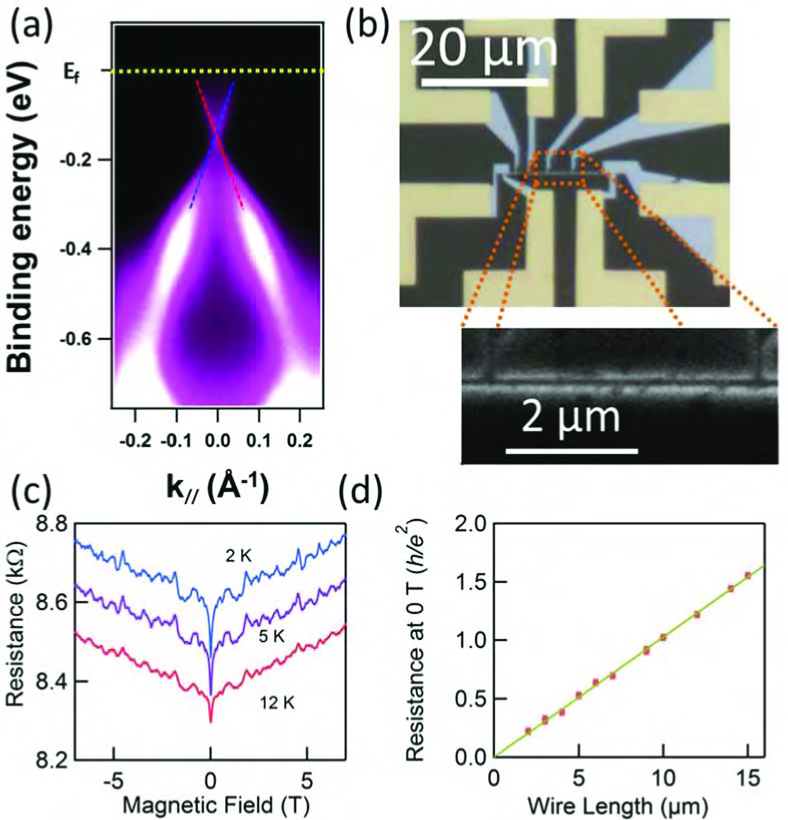
We grew a 20 nm-thick Bi2Se3 thin film by molecular beam epitaxy (MBE) on a sapphire substrate, as described previously Chang et al. (2011). We used the same thin film as in the previous report Matsuo et al. (2012). The thickness of the film was equivalent to 20 quintuple layers, which is enough to allow the surface state to emerge Zhang et al. (2010); Kim et al. (2011). Angle-resolved photoemission spectroscopy (ARPES) measurement was used to evaluate the electron band structure below the Fermi energy level in momentum-energy space, as shown in Fig. 1(a) Matsuo et al. (2012). This result shows the linear dispersion relation of the Dirac electrons on the surface, guaranteeing that our thin film is 3DTI. The Fermi energy level is located 150 meV above the Dirac point and nearly in the bottom edge of the bulk conduction band owing to natural doping by Se vacancies Xia et al. (2009).
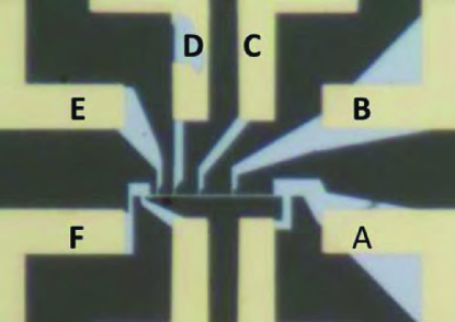
We deposited a 30 nm-thick amorphous Se layer in situ to protect the Bi2Se3 against water or oxidation that could decrease electron mobility Butch et al. (2010); Analytis et al. (2010). We fabricated wide and narrow wires using electron beam lithography. The wide one and the narrow one have 10 m width and 100 nm width, respectively. Then we deposited Ti (5 nm) and Au (100 nm) as electrodes. Figure 1(b) shows an optical image of the 100 nm-wide wire and a scanning electron microscope (SEM) image of an enlarged section of the wire; as can be seen, the edge of the wire is smooth enough to safely assume that its width is constant. In order to determine the thin film parameters, we measured the magnetic-field dependence of the longitudinal and Hall resistances of the 10 m width wire (Hall bar) at 13 different temperatures between 2 and 20 K. We also measured the magnetic-field dependence of the resistance of the 100 nm-width wire at 2, 5, and 12 K. The 100 nm-width wire had six electrodes, spaced at intervals of 1, 2, 3, 4, and 5 m, respectively, as shown in Fig. 1(b) to detect voltage difference, and two electrodes to inject current.
We obtained experimental results from wires with lengths varying from 2 to 15 m by changing voltage probe combinations. All measurements were carried out using the standard lock-in technique.
III Results and Discussions
III.1 Characterization of Bi2Se3 thin film
Based on results obtained from the 10 m-width Hall-bar sample, we were able to determine several relevant parameters. The carrier is n-type and the carrier density is , which does not depend on temperature below 20 K. Additionally, the temperature dependence of the resistance was found metallic.
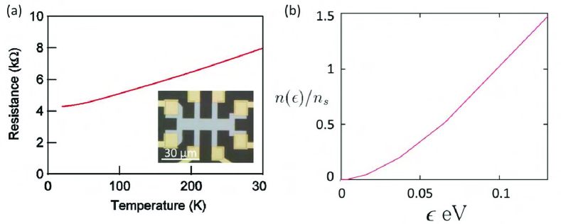
We show the resistance as a function of temperature between 20 K and 300 K in Fig. 2(a). The bulk gap of Bi2Se3 is about 0.3 eV, so that, if the Fermi energy was located in the bulk gap, the temperature dependence should be insulating. This means that our thin film was heavily n-doped semiconductor and bulk conduction mainly contributes to the transport. Based on the temperature dependence of the carrier density and resistance, we conclude that the thin film is metallic and its carriers mainly come from the bulk conduction band. This can be explained by the n-doping due to the oxidation in the air, the contamination on the microfabrication process or band bending near the interface by the substrate Chang et al. (2011); Zhang et al. (2010). For this reason, we could use a parabolic dispersion relation to calculate several relevant parameters such as the diffusion coefficient and the thermal diffusion length as follows.
III.2 Derivation of the thermal diffusion length
The mobility and the diffusion coefficient, , are Vs and , respectively; to calculate the diffusion coefficient, we used the effective mass 0.23 Stordeur et al. (1992). The thermal diffusion length is 127, 80, and 52 nm at 2, 5, and 12 K, respectively. Due to finite thickness of the sample, electrons occupy several subbands, each of which has different Fermi wave number. We take into account the subband occupation, and estimate from the weighted average over the subbands as seen below.
First, we calculated the subband energies. The thickness is nm and the subband energy can be written by
where represents the index of subband. The Fermi wavenumber for each subband is
with the 2D density of state per area, and the Fermi energy.
To determine how many subbands are filled for the experimentally estimated carrier density , we express the carrier density as a function of energy,
| (1) |
where we have assumed zero temperature. is the step function. The Fermi energy of our thin film is obtained by equating cm-2. Figure 2(b) shows the result of calculation of , from which the Fermi energy of our thin film is estimated as eV, which is smaller than the eV but greater than eV. This means that subbands with are occupied. From the Fermi energy, we can calculate the occupation of subbands as and obtain and .
The Fermi wavenumber used to estimate the diffusion constant is now defined by weighted average over subbands,
| (2) | |||||
| (3) |
The scattering time, s, is estimated from the mobility via . From and , the diffusion constant is estimated as
We used this diffusion constant to calculate the thermal diffusion length.
III.3 Coherence length of the wide Hall-bar sample
In this paper, we have discussed the quantum interference effect of Bi2Se3, so that it is helpful to refer to the coherence length in the two-dimensional system of Bi2Se3. We measured the weak anti-localization effect of the wide Hall-bar sample, whose width is 10 m, between 2 K and 20 K.
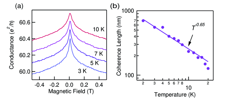
In Fig. 3(a), the magnetoconductance around 0 T at 3, 5, 7 and 10 K are shown. The vertical axis shows the data at 3 K; the other data are incrementally shifted upward by 0.1 for clarity. Then, we deduced the coherence length, , using Hikami-Larkin-Nagaoka formula (HLN formula) Hikami et al. (1980).
| (4) |
is defined by . Figure 3(b) represents the coherence length as a function of temperature. The dots show the coherence length deduced from the WAL effect. The solid line is the fit to a power function, whose exponent is -0.65. In two dimensional system, the coherence length as a function of temperature is theoretically explained by if the decoherence mechanism is dominated by electron-electron interaction Altshuler et al. (1982). Our result is quite similar to the predicted value.
Our estimate of the prefactor in Eq. (4) is . In the case of a two-dimensional system with strong spin-orbit interaction, should be equal to -0.5, which is consistent with our result. Another group reported that this prefactor becomes equal to as the coupling between the bulk and surface states becomes smaller, because the upper surface state is not hybridized to the bulk state and contribute to the conductance independently Steinberg et al. (2011). Our estimate of indicates the main contribution is from the bulk states.
III.4 Wire-length dependence of the fluctuation amplitude
Results were then obtained for the 100 nm-width wire, as can be seen in Fig. 1(c), which shows the magnetic field dependence of the resistance of the 3 m-length wire at 2, 5, and 12 K. Two important features of the resistance can be noted from the figure: there is a dip at around 0 T originating from the WAL effect; and there is magnetoresistance fluctuation in the entire magnetic field region. Figure 1(d) shows the relationship between the resistances at 0 T and 12 K and the wire length; the points and the solid line represent the experimental data and the result of their linear fitting to wire length, respectively. From the figure it can be clearly seen that the samples satisfy Ohm’s law on average and thus can be regarded as a system in weak disorder limit. This linearity guarantees that they are uniform enough to investigate their wire-length dependence of the fluctuation in the resistance.
In mesoscopic samples, UCF, namely, the conductance fluctuation of the order of occurs due to the difference of how the electron wave function interferes when the electron passes through the sample Stone (1985); Lee and Stone (1985); Altshuler (1985); Lee et al. (1987); Akkermans and Montambaux (2007). The magnetic field can add the phase via the vector potential and can change the interference, causing the conductance fluctuation as a function of magnetic field. For instance, when the phase coherence length of a quasi-1D system is finite and smaller than the sample length, self-averaging will reduce the amplitude of fluctuation by the ratio of the coherence length, , to the wire length, . When the thermal diffusion length, , is smaller than the coherence length, , the amplitude will be reduced through energy averaging by the ratio . In the case of a quasi-1D system with , the amplitude of UCF, , follows Akkermans and Montambaux (2007); Beenakker and van Houten (1991)
| (5) |
where in the presence of spin-orbit scattering and under broken time reversal symmetry. Below, we confirm that the conductance fluctuation in Bi2Se3 is proportional to and estimate the proportionality coefficient in order to verify the origin of conductance fluctuation in Bi2Se3.
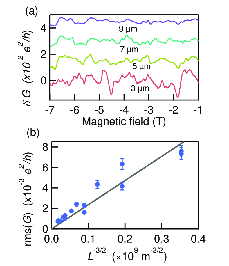
As can be seen in Fig. 1(c), the resistance in a sample fluctuates as the magnetic field is swept; we found that this fluctuation is reproducible regardless of the magnetic sweep direction. In order to isolate the fluctuation component, , for analysis, we subtracted the linear and parabolic components of the magnetoresistance as background. As examples, of the 100 nm-width wires of lengths 3, 5, 7, and 9 m at 2 K is shown in Fig. 4(a), in which it can be seen that the amplitude of fluctuation becomes smaller as the wire becomes longer. In order to ensure that this tendency is consistent with conventional UCF theory, a plot of rms at 2 K as a function of in Fig. 4(b) shows that the amplitude is indeed proportional to , as predicted by the theory.
III.5 Coherence length of quasi-1D wires
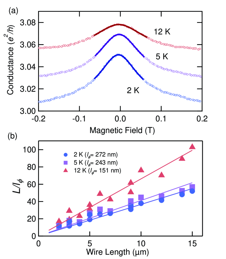
To get more quantitative results about the amplitude of the fluctuation, we analyzed the conductance peak around 0 T, which comes from the WAL effect, and deduce the coherence lengths. The circles in Fig. 5(a) show the experimentally obtained conductance of the 3 m-length wire at 2, 5, and 12 K as a function of the magnetic field near 0 T. We then fitted the data to the WAL formula for a quasi-1D system Akkermans and Montambaux (2007):
| (6) |
where is the flux quantum and is the wire width, and estimated the ratio . The results of this fitting are represented by the solid curves in Fig. 5(a). Here, the fitting range is restricted by the condition that the magnetic length is larger than the width nm, a magnetic length range based on the constraint that the magnetic flux through a phase coherent area is less than one flux quantum. It can be seen from this that the magnetoconductance of a quasi-1D Bi2Se3 wire is accurately explained by the WAL theory. The ratio is plotted as a function of wire length in Fig. 5(b). Here, the typical values of coherence length, as derived from the proportionality coefficient, are , and nm at , and K, respectively. The observed deviation from straight lines demonstrates that depends somewhat on the configuration of the voltage probes. We show the probe configurations and list the values of used for rescaling the -axis of Fig. 7 in Table 1. The probe configurations are shown in Fig. 6.
| probe | (m) | () (2K) | () (5K) | () (12K) |
|---|---|---|---|---|
| A-B | 5.0 | 19.2 (260) | 25.9 (192) | 31.1 (160) |
| A-C | 9.0 | 31.0 (290) | 35.3 (255) | 50.7 (178) |
| A-D | 12.0 | 41.5 (289) | 46.2 (260) | 70.3 (170) |
| A-E | 14.0 | 48.1 (291) | 52.4 (267) | 89.4 (157) |
| A-F | 15.0 | 52.0 (288) | 56.8 (264) | 102.9 (146) |
| B-C | 4.0 | 14.3 (280) | 16.4 (245) | 23.2 (172) |
| B-D | 7.0 | 26.3 (266) | 29.0 (241) | 42.4 (165) |
| B-E | 9.0 | 35.3 (255) | 40.6 (222) | 61.6 (146) |
| B-F | 10.0 | 37.9 (263) | 44.8 (223) | 76.0 (132) |
| C-D | 3.0 | 11.8 (255) | 13.5 (222) | 19.0 (158) |
| C-E | 5.0 | 24.8 (202) | 26.5 (188) | 36.1 (139) |
| C-F | 6.0 | 25.4 (236) | 30.9 (194) | 48.7 (123) |
| D-E | 2.0 | 11.6 (173) | 11.9 (168) | 16.6 (120) |
| D-F | 3.0 | 17.3 (174) | 17.9 (167) | 29.1 (103) |
| D-E* | 2.0 | 11.5 (174) | 11 (180) | 17.0 (118) |
III.6 Quantitative study of the fluctuation amplitude
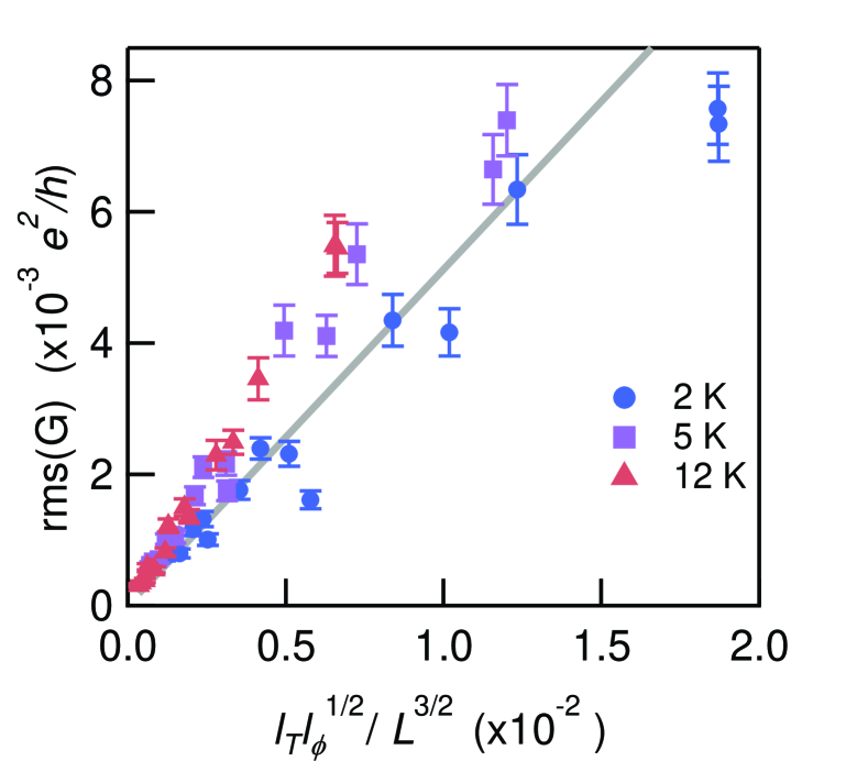
As a result of the WAL effect, the coherence length will be longer than the thermal diffusion length, which should cause UCF to arise from self averaging and energy averaging; correspondingly, the UCF amplitude should satisfy the relation expressed in Eq. (5). The values of rms() at various temperatures as a function of are shown in Fig. 7, where the circles, squares, and triangles represent data obtained at 2, 5, and 12 K, respectively. We note that, instead of the mean value estimated from the proportionality coefficient of the plot in Fig. 5(b), the value of estimated by fitting to the WAL formula (Fig. 5(a) and Eq. (6)) is used here (see Table 1).
As shown in Fig. 7, the amplitude of conductance fluctuation is proportional to , which is consistent with Eq. (5) and provides reliable evidence that the origin of the conductance fluctuation is UCF.
We next discuss the value of the coefficient in Eq. (5), for which we estimated a value of by the fitting rms() to a linear function of , as shown in Fig. 7. This is consistent with the fact that the fluctuation originates from UCF. Our result of the coefficient , however, is less than the theoretical value, Akkermans and Montambaux (2007). This discrepancy may be caused by the fact that the condition in the formula Eq. (5) is not closely satisfied. Alternatively, the deviation can be explained in terms of specific properties of the topological insulator; in either case, further study is needed to clarify the situation.
III.7 Conclusion
Together with our previous work Matsuo et al. (2012), this study very strongly supports the hypothesis that conductance fluctuation in Bi2Se3 originates from UCF. Our work has also demonstrated the transport properties of electrons in the bulk conduction band of 3DTI; this kind of understanding is necessary in determining the transport properties of disordered Dirac and Weyl electrons Kobayashi et al. (2013).
In this study, we investigated the transport properties of Bi2Se3 wires of various lengths, determining that the amplitude of conductance fluctuation is proportional to with a proportionality constant not far from the value predicted by UCF theory. This result constitutes reliable evidence that the conductance fluctuation in this material originates from UCF.
This work was partially supported by the JSPS Funding Program for Next Generation World Leading Researchers (GR058), KAKENHI No. 23540376, and Grant-in-Aid for Scientific Research on Innovative Areas ”Fluctuation & Structure” (No.25103003) from the Ministry of Education, Culture, Sports, Science, and Technology of Japan.
References
- Hasan and Kane (2010) M. Z. Hasan and C. L. Kane, Rev. Mod. Phys. 82, 3045 (2010).
- Kane and Mele (2005) C. L. Kane and E. J. Mele, Phys. Rev. Lett. 95, 146802 (2005).
- Fu and Kane (2007) L. Fu and C. L. Kane, Phys. Rev. B 76, 045302 (2007).
- Hsieh et al. (2008) D. Hsieh, D. Qian, L. Wray, Y. Xia, Y. S. Hor, R. J. Cava, and M. Z. Hasan, Nature (London) 452, 970 (2008).
- Yazyev et al. (2010) O. V. Yazyev, J. E. Moore, and S. G. Louie, Phys. Rev. Lett. 105, 266806 (2010).
- Akhmerov et al. (2009) A. R. Akhmerov, J. Nilsson, and C. W. J. Beenakker, Phys. Rev. Lett. 102, 216404 (2009).
- Checkelsky et al. (2009) J. G. Checkelsky, Y. S. Hor, M.-H. Liu, D.-X. Qu, R. J. Cava, and N. P. Ong, Phys. Rev. Lett. 103, 246601 (2009).
- Checkelsky et al. (2011) J. G. Checkelsky, Y. S. Hor, R. J. Cava, and N. P. Ong, Phys. Rev. Lett. 106, 196801 (2011).
- Qu et al. (2011) F. Qu, F. Yang, J. Chen, J. Shen, Y. Ding, J. Lu, Y. Song, H. Yang, G. Liu, J. Fan, Y. Li, Z. Ji, C. Yang, and L. Lu, Phys. Rev. Lett. 107, 016802 (2011).
- Chen et al. (2011) J. Chen, X. Y. He, K. H. Wu, Z. Q. Ji, L. Lu, J. R. Shi, J. H. Smet, and Y. Q. Li, Phys. Rev. B 83, 241304 (2011).
- Wang et al. (2011) J. Wang, A. M. DaSilva, C.-Z. Chang, K. He, J. K. Jain, N. Samarth, X.-C. Ma, Q.-K. Xue, and M. H. W. Chan, Phys. Rev. B 83, 245438 (2011).
- Steinberg et al. (2011) H. Steinberg, J.-B. Laloë, V. Fatemi, J. S. Moodera, and P. Jarillo-Herrero, Phys. Rev. B 84, 233101 (2011).
- Chen et al. (2010) J. Chen, H. J. Qin, F. Yang, J. Liu, T. Guan, F. M. Qu, G. H. Zhang, J. R. Shi, X. C. Xie, C. L. Yang, K. H. Wu, Y. Q. Li, and L. Lu, Phys. Rev. Lett. 105, 176602 (2010).
- Liu et al. (2011) M. Liu, C.-Z. Chang, Z. Zhang, Y. Zhang, W. Ruan, K. He, L.-l. Wang, X. Chen, J.-F. Jia, S.-C. Zhang, Q.-K. Xue, X. Ma, and Y. Wang, Phys. Rev. B 83, 165440 (2011).
- Kim et al. (2011) Y. S. Kim, M. Brahlek, N. Bansal, E. Edrey, G. A. Kapilevich, K. Iida, M. Tanimura, Y. Horibe, S.-W. Cheong, and S. Oh, Phys. Rev. B 84, 073109 (2011).
- Onose et al. (2011) Y. Onose, R. Yoshimi, A. Tsukazaki, H. Yuan, T. Hidaka, Y. Iwasa, M. Kawasaki, and Y. Tokura, Appl. Phys. Express 4, 083001 (2011).
- Taskin et al. (2012) A. A. Taskin, S. Sasaki, K. Segawa, and Y. Ando, Phys. Rev. Lett. 109, 066803 (2012).
- Bao et al. (2012) L. H. Bao, L. He, N. Meyer, X. F. Kou, P. Zhang, Z. G. Chen, A. V. Fedorov, J. Zou, T. M. Riedemann, T. A. Lograsso, K. L. Wang, G. Tuttle, and F. X. Xiu, Sci. Rep. 2, 726 (2012).
- Lu and Shen (2011) H.-Z. Lu and S.-Q. Shen, Phys. Rev. B 84, 125138 (2011).
- Matsuo et al. (2012) S. Matsuo, T. Koyama, K. Shimamura, T. Arakawa, Y. Nishihara, D. Chiba, K. Kobayashi, T. Ono, C.-Z. Chang, K. He, X.-C. Ma, and Q.-K. Xue, Phys. Rev. B 85, 075440 (2012).
- Li et al. (2012) Z. Li, T. Chen, H. Pan, F. Song, B. Wang, J. Han, Y. Qin, X. Wang, R. Zhang, J. Wan, D. Xing, and G. Wang, Sci. Rep. 2, 595 (2012).
- Stone (1985) A. D. Stone, Phys. Rev. Lett. 54, 2692 (1985).
- Lee and Stone (1985) P. A. Lee and A. D. Stone, Phys. Rev. Lett. 55, 1622 (1985).
- Altshuler (1985) B. Altshuler, JETP Lett. 41, 648 (1985).
- Lee et al. (1987) P. A. Lee, A. D. Stone, and H. Fukuyama, Phys. Rev. B 35, 1039 (1987).
- Akkermans and Montambaux (2007) E. Akkermans and G. Montambaux, Mesoscopic Physics with Electrons and Photons (Cambridge University Press, Cambridge, England, 2007).
- Rossi et al. (2012) E. Rossi, J. H. Bardarson, M. S. Fuhrer, and S. Das Sarma, Phys. Rev. Lett. 109, 096801 (2012).
- Adroguer et al. (2012) P. Adroguer, D. Carpentier, J. Cayssol, and E. Orignac, New Journal of Physics 14, 103027 (2012).
- Chang et al. (2011) C. Z. Chang, K. He, M. H. Liu, Z. C. Zhang, X. Chen, L. L. Wang, X. C. Ma, Y. Wang, and Q. K. Xue, SPIN 1, 21 (2011).
- Zhang et al. (2010) Y. Zhang, K. He, C.-Z. Chang, C.-L. Song, L.-L. Wang, X. Chen, J.-F. Jia, Z. Fang, X. Dai, W.-Y. Shan, S.-Q. Shen, Q. Niu, X.-L. Qi, S.-C. Zhang, X.-C. Ma, and Q.-K. Xue, Nat. Phys. 6, 584 (2010).
- Xia et al. (2009) Y. Xia, D. Qian, D. Hsieh, L. Wray, A. Pal, H. Lin, A. Bansil, D. Grauer, Y. S. Hor, R. J. Cava, and M. Z. Hasan, Nat. Phys. 5, 398 (2009).
- Butch et al. (2010) N. P. Butch, K. Kirshenbaum, P. Syers, A. B. Sushkov, G. S. Jenkins, H. D. Drew, and J. Paglione, Phys. Rev. B 81, 241301 (2010).
- Analytis et al. (2010) J. G. Analytis, J.-H. Chu, Y. Chen, F. Corredor, R. D. McDonald, Z. X. Shen, and I. R. Fisher, Phys. Rev. B 81, 205407 (2010).
- Stordeur et al. (1992) M. Stordeur, K. K. Ketavonc, A. Priemuth, H. Sobotta, and V. Riede, phys. stat. sol. (b) 169, 505 (1992).
- Hikami et al. (1980) S. Hikami, A. I. Larkin, and Y. Nagaoka, Prog. Theor. Phys. 63, 707 (1980).
- Altshuler et al. (1982) B. L. Altshuler, A. G. Aronov, and D. E. Khmelnitskii, J. Phys. C: Solid State Phys. 15, 7367 (1982).
- Beenakker and van Houten (1991) C. Beenakker and H. van Houten, Solid State Physics 44, 1 (1991).
- Kobayashi et al. (2013) K. Kobayashi, T. Ohtsuki, and K.-I. Imura, Phys. Rev. Lett. 110, 236803 (2013).