Production and Characterisation of SLID Interconnected n-in-p Pixel Modules with 75 Micrometer Thin Silicon Sensors
Abstract
The performance of pixel modules built from 75 micrometer thin silicon sensors and ATLAS read-out chips employing the Solid Liquid InterDiffusion (SLID) interconnection technology is presented. This technology, developed by the Fraunhofer EMFT, is a possible alternative to the standard bump-bonding. It allows for stacking of different interconnected chip and sensor layers without destroying the already formed bonds. In combination with Inter-Chip-Vias (ICVs) this paves the way for vertical integration. Both technologies are combined in a pixel module concept which is the basis for the modules discussed in this paper.
Mechanical and electrical parameters of pixel modules employing both SLID interconnections and sensors of 75 micrometer thickness are covered. The mechanical features discussed include the interconnection efficiency, alignment precision and mechanical strength. The electrical properties comprise the leakage currents, tuning characteristics, charge collection, cluster sizes and hit efficiencies. Targeting at a usage at the high luminosity upgrade of the LHC accelerator called HL-LHC, the results were obtained before and after irradiation up to fluences of .
keywords:
Pixel detector , Solid Liquid InterDiffusion , 3D-Integration , Thin sensors , HL-LHC , Radiation hardness1 Future Pixel Modules and 3D-Integration Technology
The ATLAS pixel detector [1] is made of three barrel layers with an innermost radius of 50.5 mm and three end-cap discs on each side of the detector. The pixel modules used consist of 16 FE-I3 read-out chips [2] which are interconnected via the solder bump bonding technique [3] to a 250 m thick n-in-n planar silicon sensor. The size of individual pixel cells is 50 m 400 m. Sensors and read-out chips are specified for a maximum fluence111The fluences for proton and neutron irradiation are rescaled to the damage expected for 1 MeV neutrons, indicated by . of and a dose of 500 kGy.
A large upgrade to the LHC accelerator chain - called HL-LHC - is currently planned to start taking data in 2024. The peak luminosity will eventually be increased up to 5 cm-2s-1 [4]. To maintain the detector performance, several upgrades of the ATLAS pixel detector are planned. The first of these upgrades, the so called Insertable B-Layer (IBL) [5], is a new fourth pixel layer, which is planned to be mounted on a new smaller beam pipe at a radius of 32 mm, and to be operational by the end of 2014. Due to the smaller radius, the modules cannot overlap along the beam direction as they do for the present ATLAS pixel detector. Thus, the active fraction of the new pixel modules was increased [6, 7, 8]. Additionally, the harsher radiation environment and the higher occupancy demanded for a new read-out chip, the FE-I4 [9], specified up to a received fluence of and with a reduced pixel size of 50 m 250 m. Furthermore, the number of pixel cells increased from 2880 to 26880 per chip. While it is expected that the upgraded pixel detector retains sufficient tracking capabilities until around 2024, a full replacement of the tracking detector is required afterwards.
The current baseline detector upgrade layout [10] consists of four pixel layers at a minimal radius of about 39 mm, supplemented by six pixel discs at each of the forward regions, extending to a pseudo-rapidity of about . Given the corresponding extreme radiation levels of up to in the innermost layer a new generation of read-out chips will be needed for the inner layers, featuring even smaller pixels to cope with the otherwise largely increased pixel occupancy.
1.1 Module Concept
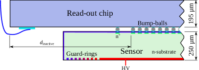
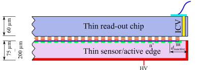
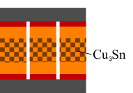
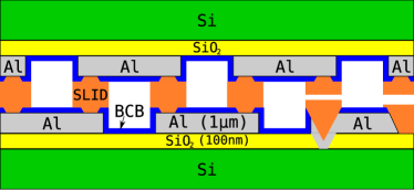
To answer the challenges of this upgrade, a module concept for the pixel layers is investigated, which employs several novel technologies in the field of pixel detectors: n-in-p pixel sensors are thinned using a process [11] developed at the Max-Planck-Gesellschaft Halbleiterlabor (MPG-HLL), and connected via the Fraunhofer EMFT [12] Solid Liquid Inter-Diffusion (SLID) technology to the read-out electronics, where the signals are routed via Inter-Chip-Vias (ICVs). Additionally, the active fraction is maximised by an optimised guard ring design in combination with or without implanted sensor sides [13]. In Figure 1 the schematics of 1 the present and 1 the investigated concept are shown.
Advantages of this approach are: the n-in-p technology allows for single sided processing of wafers resulting in a lower cost, which is of special importance for the large areas foreseen in future pixel detector upgrades. In addition, the radiation hardness is comparable to the presently used n-in-n technology [14, 15]. Thinner sensors not only reduce the material budget and therefore multiple scattering but also, at the same applied bias voltage, they exhibit higher electric fields than thicker devices. This leads to a high charge collection efficiency (CCE) after high radiation doses at moderate bias voltages [16, 17, 15]. While on the sensor side the inactive area is removed by activated edges, in a 3D compliant design of the pixel electronics, ICVs could eventually avoid the need for the cantilever area where presently the wire bonding pads are located. Combining these ICVs with SLID interconnections enables fully 3D-integrated modules. Furthermore, SLID interconnections could allow for a pitch reduction with respect to the 50 m pitch limit given by the solder bump bonding.
In this paper, the results on the SLID interconnection and thin sensor aspects of this module concept are presented and discussed. Some preliminary results were already given in [18, 19, 20, 21, 22] as well as in the PhD-theses [23, 15]. All SLID modules presented here use the FE-I2 [24] ATLAS readout chip that has the same footprint as the FE-I3 chip. The two chips only differ in minor details, e. g. they need slightly different chip analogue and digital voltages documented in [25]. These differences are not relevant for the work presented in this paper. Consequently, in the following no distinction is made and both chips are referred to as FE-I3 chips. Further results on the other technologies used in the module concepts, as n-in-p sensors, active edge pixel devices and ICVs, can be found in [26, 13, 15, 23].
In the presentation of the results first a short introduction to SLID will be given, followed by the technical and mechanical results. Finally, the performance for prototype pixel modules employing SLID and 75 m thick sensors will be discussed.
1.2 Solid-Liquid InterDiffusion
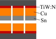
SLID is a class of interconnection techniques, where the formation of the interconnection takes place at temperatures significantly lower than those the connections can tolerate afterwards without dissolving. The concept was introduced in the 1960s [27, 28] and is based on binary, ternary, or even higher-order metal systems, where one low-temperature melting metal is coated on a high-temperature melting core. By bringing the temperature of the metal system above the melting point of the low-temperature melting metal and applying high pressure, this metal dissolves and diffuses into the high-temperature melting metal. Inter-metallic compounds with melting points above the heating temperature are formed by the two metals and the liquid phase solidifies. While many different metal systems are known to form SLID bonds, certain constraints apply when using this technique in real applications [29]. For example, the melting point of the low-temperature melting metal should be below 400 , which is the maximum temperature most Application Specific Integrated Circuits (ASICs) can withstand. In the presented module concept, the SLID process developed by the EMFT is used. The process steps are shown in Figure 2. In this approach Sn ( ) is used as the low-temperature melting component and Cu ( ) as the high-temperature melting component. Out of these, Cu3Sn ( ) and Cu6Sn5 ( ) are formed. The high melting point of the interconnecting alloy opens the possibility of subsequent stacking of additional SLID-interconnected layers, but at the same time inhibits reworking of badly connected devices.
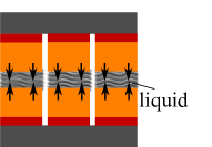
A comparison of the process flows of the conventional bump bonding techniques and SLID, shown in Figure 3, reveals further advantages and challenges. While the first step is a patterned electroplating step needed for the deposition of the Cu and Sn, which is similar for both technologies, the so-called reflow step is not needed to form SLID interconnections. In the reflow step, the alloy or metal, e. g. PbSn or In that are used in the bump bonding process is melted; the surface tension leads to solder ball formation. Since the diameter of the balls is determined by the initial pad size, all bump-bond connections have to be of equal size to form good connections (compare 3rd connection to the neighbouring ones in Figure 3). In contrast, a SLID bond can have an arbitrary shape and size, with the only constraint that its dimensions exceed 5 m by 5 m. Additionally, the reduction of one process step is expected to lower the costs once the process is established in industry. In the interconnection-step the read-out chip and the sensor are brought together.
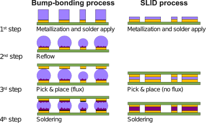
In the bump-bonding process a built-in self alignment due to the surface tension of the bump-balls is exploited, while the SLID interconnection has to rely on the pick-and-place precision for the placement of the read-out chips on the handle wafer, when the technique is applied in the chip-to-wafer approach. If a high accuracy can be achieved in the pick-and-place procedure, the pitch of the SLID connections can be as low as approximately 20 m [30], which is not possible for the bump-bonding offered for industrial applications. In the final step, the actual bond is formed by pressing the two layers together. While a non functional bump-bonded module with a broken read-out chip or sensor can be separated again for repair by reheating this is not possible for SLID assemblies, due to the higher temperature needed.
Other innovative interconnection technologies are presently investigated for pixel modules for use in high energy physics experiments. These are the Ziptronix Direct Bond Interconnect (DBI) oxide bonding and the copper thermo-compression [31], both under evaluation at Fermilab, and also the copper pillar interconnects [32], offered by CEA-LETI [33].
2 Technical Aspects and Mechanical Properties
2.1 Influence of the SLID Process on Silicon Sensors
Since the SLID interconnection was only known to work with integrated circuit (IC) devices, a production of diodes subjected to the SLID metallization and temperature treatment was carried out. Compared to IC devices, the performance of sensors that are usually made from high resistivity silicon, is much more sensitive to high leakage currents caused by a diffusion of copper atoms into the silicon bulk. In the SLID process, to prevent diffusion of copper into the silicon bulk a barrier layer of Titanium Tungsten (TiW) is needed. The diodes were used to verify the functionality of this TiW diffusion barrier with thin silicon sensors.
To model both sides of the SLID metallization, two 6-inch wafers with various thin p-in-n diodes were produced. The sensor concept uses an SOI technology with an active sensor wafer that can be thinned to a desired thickness, and that is oxide bonded to a handle wafer for mechanical stability. The p-in-n option was chosen since no difference in the sensitivity of p-in-n and n-in-p sensors towards copper atoms is expected and the n-type wafers were easily procurable. The implemented diodes have an area of mm2 with different guard-ring designs and are thinned down with the HLL thinning technology to an active thickness of m. Together with the handle wafer, the total thickness of the wafers is m.
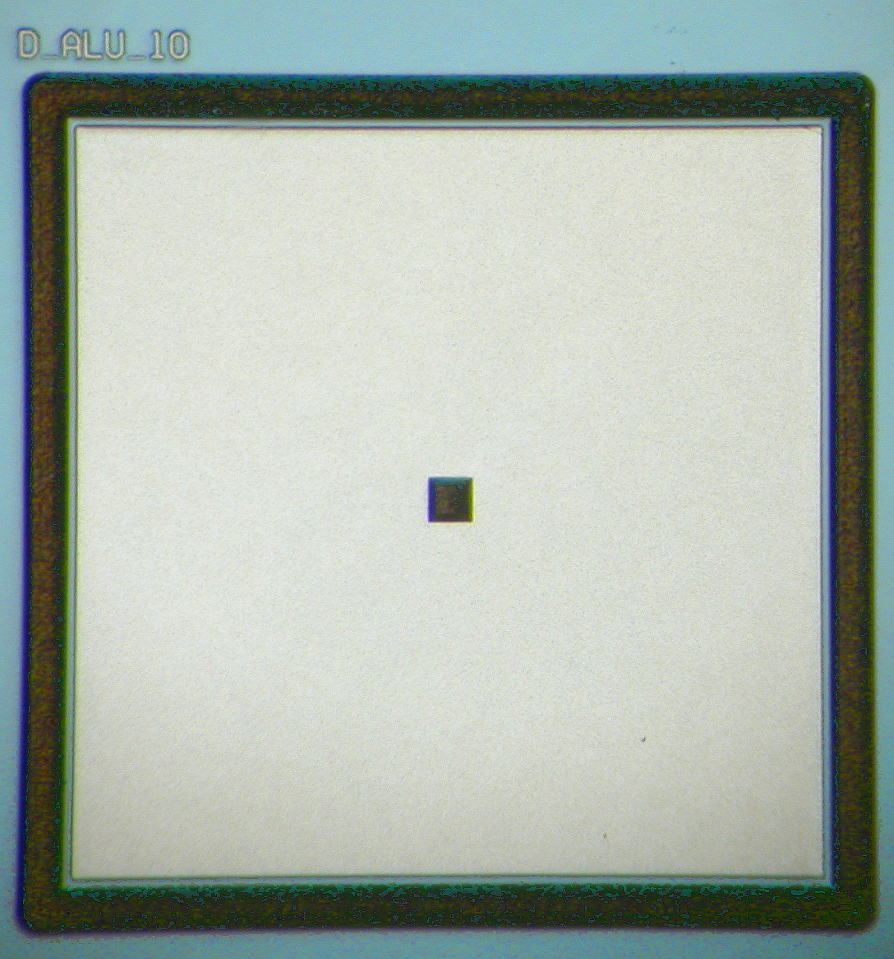
On both wafers shown in Figure 4, a nm thin layer of TiW was applied to the aluminium contact pads of all diodes, followed by an electroplating of Cu. For the first wafer, shown in Figure 4, the thickness of the Cu is around m and no further layers are applied. The second wafer, which is displayed in Figure 4, was equipped with m of Cu and m of Sn. Hence, both sides of the SLID metallization are replicated separately. The reduced thickness of the Cu layer on the first wafer of m, compared to the m used in the SLID interconnection, is assumed to be sufficient for an investigation of the full impact caused by a possible copper diffusion. For the second wafer, the thickness of the Sn was chosen to be a little less than half of the m used in the SLID process. This ensures, that the Sn can be completely absorbed by the single Cu layer of the wafer.
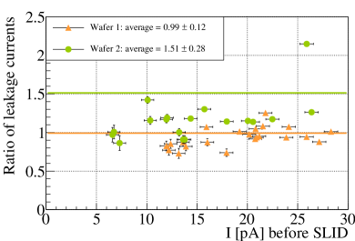
In a first step the leakage currents of the diodes were measured before the application of any SLID metal layers. The same diodes were measured after the application of the TiW and Cu for the first wafer and TiW, Cu, and Sn for the second wafer. Shown in Figure 5 are the ratios of these leakage currents of the measured diodes of both wafers obtained after various production steps and at V. The currents were determined by a linear fit to the plateau region of the leakage current characteristics. The uncertainties assigned are the combination of the one standard deviation uncertainties calculated from the measurement uncertainties of the Keithley-487 picoamperemeter [34] and the fit uncertainties. The leakage currents of the diodes on both wafers do not increase to a level that could be dangerous for the sensor operation. On wafer 1, the average current of the diodes at V is unchanged while on wafer 2, it increases by about 51.
Removing the outlier (i.e. the diode of wafer 2 in Figure 5 that has a ratio of leakage currents of about 2.2) from the analysis, which had a defect not related to the SLID interconnection, an average increase of only 18 is found. These measurements show that during the application of the SLID metallization no copper diffuses into the sensor, since this would lead to an increase of the leakage current by several orders of magnitude [35].
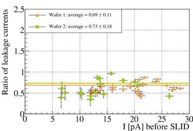
In a next step, both wafers were heated in the standard processing atmosphere to 320 for 15 min to simulate the SLID temperature treatment, and to start the Solid-Liquid InterDiffusion of the Sn into the Cu. An actual connection of the wafers was not performed. After the temperature treatment the leakage currents of the diodes showed a slight decrease, as shown in Figure 5. Compared to the measurements before any SLID processing steps, the currents are only 69 and 73 of the initial values for wafers 1 and 2, respectively. This is expected to be due to the annealing of defects in the silicon bulk caused by the applied temperature.
2.2 Alignment Precision and Interconnection Efficiency of the SLID Interconnection
One of the key performance parameters to judge the applicability of the SLID interconnection technology is its connection efficiency . It is defined as the probability that a given single SLID interconnection is successful. The corresponding inefficiency, i. e. the probability of a fault of a given connection, is the figure of merit commonly used and given in the results below. To calculate the inefficiency from measurements of structures with a group of serial SLID interconnections, a binomial probability distribution is assumed. From the number of SLID interconnections per group and the fraction of groups with all connections working,
| (1) |
is derived. The inefficiency should be as low as possible; for example it was required to be smaller than for the present ATLAS pixel modules [36].
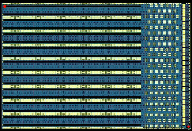
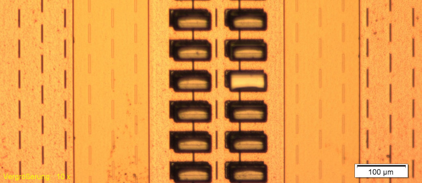
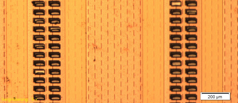
To measure of the SLID interconnection, its dependence on the alignment precision, and the sensitivity to disturbances of the device planarity, a SLID prototype production was carried out. For this, a 6-in.-wafer layout designed at the MPP, and shown in Figure 6, was used. The layout includes a total of 152 test devices, which rely solely on structured metallisation directly on the SiO2 but do not have any implants. The SLID contact positions are symmetric with respect to the -axis and hence, two of these wafers can be connected by rotating one around its symmetry axis by and placing it onto the other. Through this, the 76 devices in the northern half of one wafer, which are referred to as sensor devices, are connected to the 76 chip devices of the southern part of the other wafer.
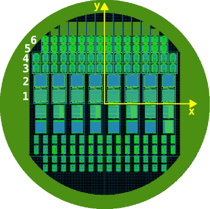
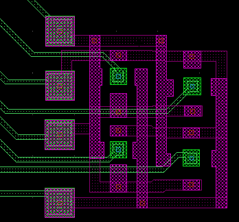
A large fraction of the area of each device is filled with daisy chains which are a serial wiring scheme of a large group of SLID interconnections in a row with alternating aluminium traces on the sensor- and chip-side, as shown in Figure 6. If a potential difference is applied to the ends of a daisy chain, a current can only flow provided all SLID interconnections are functional. Hence, a large number of SLID interconnections are tested at the same time. The daisy chains of the 76 devices of the sensor side are equipped with aluminium traces leading to contact pads for needle probes at the ends of the daisy chains. On the chip devices, there are no traces since this part of the devices is cut off during the singularisation to enable access to the contact pads of the sensor devices. Hence, after connecting two wafers only those 76 structures can be used where the sensor devices are on the lower wafer which is not cut.
Rows 1 and 2 of larger devices above the horizontal wafer axis contain daisy chains which have the same geometry as an ATLAS pixel sensor. This means that the metal traces occupy the same areas as the pixel implants do in the sensors. In addition, aluminium lines are implemented to connect every second pair of traces to form an open chain. The SLID interconnection of open chains from chip and sensor devices leads to closed, i. e. conducting chains, as shown in Figure 6. In row 1, the SLID pad size is with a small pitch of 50 m and a large pitch of 400 m. This corresponds to the SLID pad dimensions used for the prototype pixel modules discussed below. The chains of row 2 have identical pitches but the SLID pads are of similar size as the n-type implants in the ATLAS pixel sensors, i. e. . Within the smaller devices in rows 3 to 6 of the wafer, a variety of SLID pad sizes and pitches are implemented in different daisy chains. They range from with a pitch of m to with a pitch of 115 m as detailed in Table 1.
| Pad size | Pitch | Aplanarity | Connections | Inefficiency |
|---|---|---|---|---|
| measured | ||||
In addition, in rows 3 and 4 special chains are implemented which have a part, where deliberately either the SiO2 or the aluminium layer is missing. This leads to a lowering of the SLID pads by 100 nm or 1 m as illustrated on the right side of Figure 6. With these degradations of the device planarity the sensitivity of the SLID interconnection to surface imperfections is investigated.
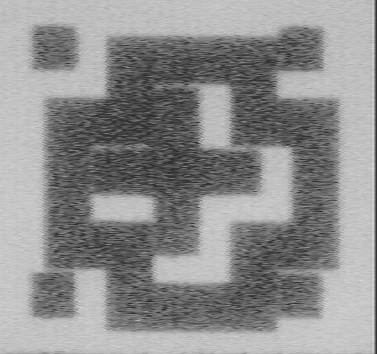
Furthermore, electrical and optical alignment structures are introduced in the devices. The electrical alignment structures consist of SLID pads that are only connected if the devices are misaligned. A section of the wafer map containing one of the alignment structures which measures a misalignment of (2.5–15) m is shown in Figure 6. The structures shown in green are located on the sensor wafer and consist of eight metallized squares, four small ones and four larger ones. The structures drawn in red are located on the chip side. Depending on the size of the misalignment different counterpart pads match, and are electrically conducting, which is verified with probe needles on external pads (not shown). In the presented case of perfect alignment, the four large square contacts of both sides are connected, while the small green square contacts have no counter part on the chip. If, as an example, a misalignment of 3 m is introduced, the lower left SLID pad in Figure 6 can contact one or two of the surrounding red structures on the chip. This forms a conducting channel which can be identified by contacting the corresponding probe pads. Since the sensor side squares will connect to different counterparts, not only the magnitude but also the direction of the misalignment can be identified. Further alignment structures on each device allow for measuring a misalignment of up to 30 m.
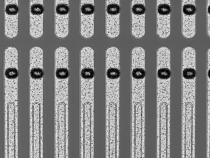
The optical alignment structures are aluminium vernier scales that are implemented partly on the sensor- and partly on the chip side of the packages, as shown in Figure 7. Using an infra-red microscope they allow to determine the relative misalignment with an accuracy of 3 m. The measurements of the SLID daisy chains were carried out with a Keithley-6517A electrometer [34], supplying a small voltage to the ends of the chains and measuring the current. Through this, also the resistance of the chains are measured and a mean resistance per SLID connection is determined. Using an infra-red microscope the relative misalignment is determined.
2.2.1 Wafer-to-Wafer Interconnection
The wafers were interconnected in a wafer-to-wafer approach. For the majority of the chains all SLID connections were functioning resulting in finite resistances ranging from to per SLID connection, where the uncertainties are the one standard deviations of the measurements from various equivalent chains. The chain resistances do not directly correlate to the size of the SLID pads but rather to the number of SLID connections per row ranging from 46 to 302 connections. This leads to the conclusion that the dominating contribution to the resistance is not caused by the SLID metal layers, but rather by the contact between them and the aluminium traces. This contact is made underneath each SLID pad by creating a circular opening with 10 m nominal diameter in the BCB passivation layer covering the whole wafer, displayed in Figure 6. The openings have the same diameter for all pads of all chains.
Table 1 summarizes the results of all daisy chain measurements and includes the total number of SLID connections tested. The SLID inefficiency is less than for most of the chain types without a deliberately introduced aplanarity. The exception are the structures of row 1 for which 24160 contacts were measured, and for which 10 out of 80 chains with 302 connections each were interrupted. In those cases, where no interrupted contacts were found, an upper limit at a 90 confidence level is reported. The smallest limit observed is , consequently higher statistics data are needed to verify that an inefficiency of less than is met by the process. Some chains have been produced without the aluminium layer below the SLID pads. This is an exaggerated situation that is much more severe than the typical thickness variations of the aluminium layer, and does not occur in real applications. Even those chains result in a connection inefficiency per pad of , clearly showing that the SLID interconnection is not severely affected by variations of the surface planarity up to 1 m.
The optical inspections of the vernier scales as well as the measurements of the electrical alignment structures showed a very good alignment accuracy of better than 5 m for the first and about (5–10) m for the second pair of interconnected wafers.
2.2.2 Chip-to-Wafer Interconnection
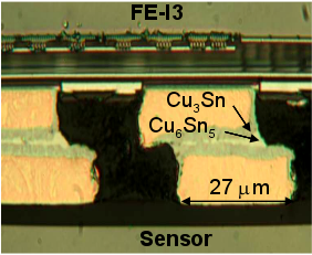
In another prototype run ATLAS FE-I3 read-out chips were interconnected to fully functional thin pixel sensors. The sensors were produced on p-bulk FZ wafer using the MPG-HLL thinning process with a final active thickness of 75 m. The specific resistivity of these wafers is kcm. A discussion of the electrical characteristics of all structures within this production can be found in [23]. The full depletion voltages were found to be () V, with the exception of one pixel device that did not reach a plateau in the leakage current, i. e. where the breakdown voltage was lower than . This corresponds to a yield of .
For the 79 pixel devices, an over depletion of up to can be reached. Finally, their leakage currents in the plateau region were determined to be below 10 nA/cm2.
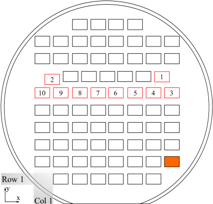
For the interconnection, operating a flip-chipping machine in a pick and place mode, in a chip-to-wafer process, a handle wafer was populated with known working read-out chips at the positions of compatible pixel structures on the sensor wafer side as indicated by the red numbered rectangles in Figure 8. Due to the high applied pressure in the process, and to achieve good precision in the pick and place process, a regular pattern of chips on the handle wafer is mandatory. Consequently, the rest of the handle wafer was populated regularly with read-out chips (indicated in black). The electroplated SLID pad structure is the same for the working and for the dummy read-out chips. An excellent alignment of the read-out chips on the handle wafer with respect to their nominal positions, known from the design of the sensor wafer, is needed, given the small pitch and SLID pad sizes in combination with the needed minimal overlap of .
Additionally, it is important that rotations of the read-out chips are below about 0.5∘. Although, a global misalignment can be corrected for by adjusting the relative position of the two wafers in the wafer-to-wafer interconnection process, these requirements demand cutting-edge pick-and-place technology.
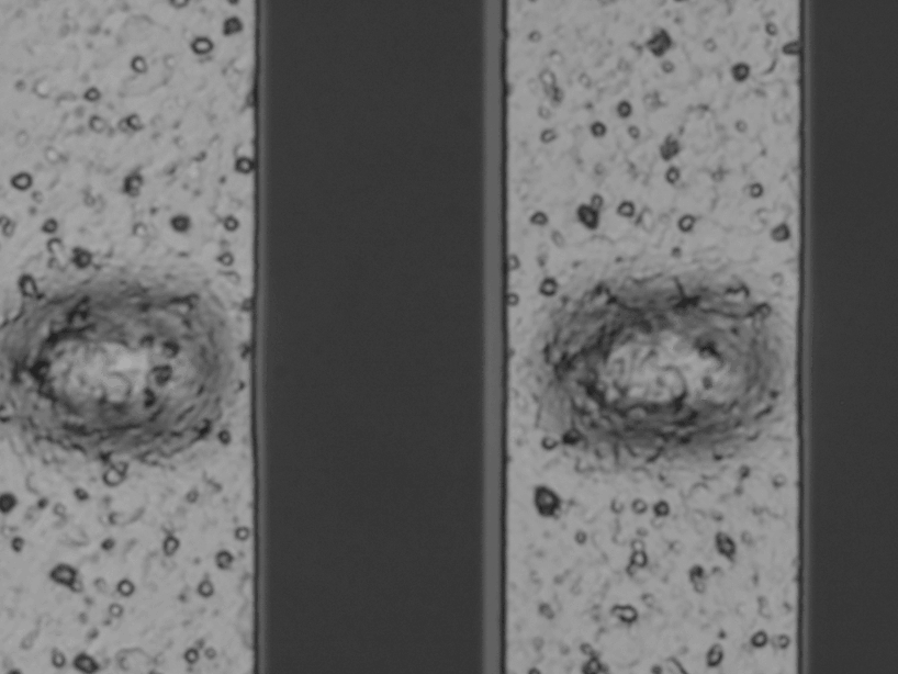
The positions of the alignment marks (cross and circle) are indicated in red in Figure 9. In Figure 9, an infra-red picture of a cross alignment mark is depicted for a connected stack. Based on these images, the quality of the alignment was determined after interconnection.
| Module | [m] | [m] | Tilt [∘] | Connected [] |
|---|---|---|---|---|
| 1 | 100 | |||
| 2 | ||||
| 3 | 100 | |||
| 4 | 44 | 73 | 0.72 | |
| 5 | ||||
| 6 | ||||
| 7 | ||||
| 8 | ||||
| 9 | ||||
| 10 | 100 |
The residual misalignment after interconnection is summarised in Table 2. In total, seven out of ten assemblies were built successfully, i. e. without shorts or open connections caused by misalignment. For the assemblies 2, 4 and 5 the misalignment is too large for the pixel assemblies to be functional. To improve the precision of the alignment for future productions, a new and more precise pick-and-place machine will be employed. Additionally, the possibility to exploit self alignment via evaporative liquid glues while populating the handle wafer is currently investigated at the EMFT [37].
Open connections were identified with a high statistics radioactive source measurement in which not connected pixel cells exhibit a low hit rate, because they can only contribute via electronic noise, but not via genuine signal. For the used statistics, and in the centre of the beam spot, around 150 hits per pixel are expected. A pixel cell is defined as connected, if it exhibits more than 50 hits. Uncertainties are assessed by varying this threshold by . The percentages of connected pixel cells per module are summarised in Table 2. While for module 1, 3 and 10 all pixel-cells are connected, module 6 exhibits around 30 of not connected pixel cells. A trend of the fraction of not connected cells to rise towards the centre of the wafer is found.
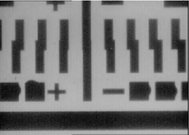
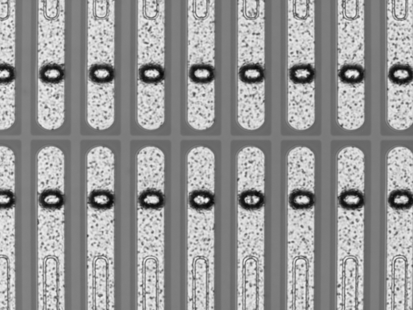
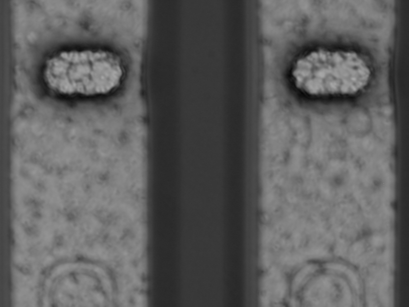
Subsequent optical re-inspections of not yet connected sensor wafers from the same production revealed that the cause for these not connected pixel cells are imperfect openings of the BCB passivation layer underneath the SLID pads that show a radial trend across the wafer similar to the one observed for the not connected cells. Photographs of such not fully opened layers are depicted in Figure 10 and Figure 10. For future module assemblies, a removal of residual BCB in the openings using an SF6 plasma descum process offered by the Fraunhofer IZM [38] was investigated. In the optical inspection after the treatment all BCB contacts were found to be fully opened. Figure 10 and Figure 10 are photographs of fully opened contacts. Thus, this is not an issue for future productions.
Another crucial factor is the stability of the connections in experimental conditions, where, in addition to high radiation levels, temperature cycles are present. Within the laboratory and during beam test measurements for all modules the numbers of not connected pixel cells did not change with numerous thermal cycles between 20 and . Furthermore, no changes after irradiation up to a fluence of were observed. This is a strong indication that SLID interconnections are radiation hard and withstand thermal cycles.
2.3 Mechanical Strength
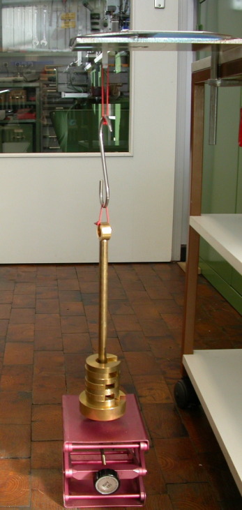
A high mechanical strength is desirable for an interconnection technology, as it eases the handling of the device, ensures that bonds do not break accidentally, and that they are stable in time. To determine the mechanical strength, a piece of plexiglass was glued onto each dummy read-out chip (black in Figure 8) in the lower half of the handle wafer. Subsequently, weight was hanged onto the plexiglass holder while the sensor wafer was stabilised in its position by a plexiglass support covering the full area except for the region around the read-out chip under study. After each increase of weight the strain was relieved using a small hoisting platform to apply the force in a controlled manner. Before adding the next weight the hoisting platform was lifted again. A photograph of the setup is depicted in Figure 11. Due to the construction, the minimum weight applied is 0.6 kg.
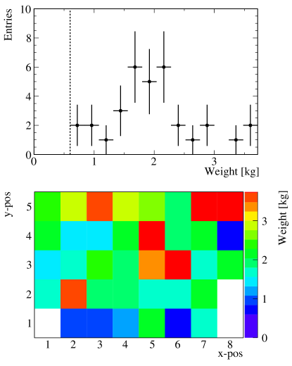
The distribution of the weight needed to break the connection between sensor and read-out chip is given in Figure 12. No systematic trend across the wafer is appreciable and the weight needed for breakage is approximately two kilograms, which corresponds to 0.01 N per SLID connection. This is of the same order of magnitude to what is found for other interconnection technologies [39, 40, 41, 42, 43]. With the exception of extreme cases of misalignment, no significant correlation between the misalignment and the connection is found.
In Figure 13 photographs of the pulled off read-out chips are shown. In almost all cases the whole SLID stack is appreciable, indicating that the weakest point of the interconnection is at the electroplated layers, i. e. layers that are similar in other technologies as for example bump bonding.
3 Electrical Properties of the Pixel Modules
In the following the performance of the successfully built pixel modules from the chip-to-wafer prototype production are discussed based on results obtained before and after irradiation. These results comprise: leakage currents, tuning properties, charge collection measurements, and in addition hit efficiencies and cluster sizes determined in beam test measurements.
3.1 IV Characteristics and Irradiation Programme
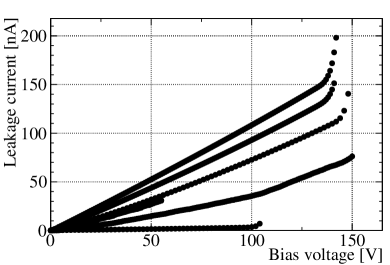
As basic functionality test, the IV characteristics of all seven modules are summarised in Figure 14. All IV characteristics were taken with the read-out chip powered, but not configured, to ensure a defined ground potential and exclude temperature changes [14]. At an over-depletion of about 10 V, i. e. at 30 V, the leakage currents are below 50 nA and thus far below the operational limit of 300 A [1].
The breakdown voltage lies for one module at 100 V, for additional four modules at or above 140 V. Additional two structures were measured only up to a bias voltage of 55 V, and no breakdown was observed. For the structures measured up to the breakdown voltage, , this corresponds to a good over-depletion ratio .
Subsequently, the modules were irradiated at the Karlsruhe Institut of Technology (KIT) with 25 MeV protons [44, 45] and at the Jožef Stefan Institute (JSI) with reactor neutrons [46]. The full irradiation programme is summarised in Table 3. The range (0.6–10) was covered mainly with reactor neutron irradiation.
| Fluence [ ] | Irradiation site | Beam test |
|---|---|---|
| 0.6 | KIT | yes |
| 0.6+0.4 | KIT | |
| 2 | JSI | yes |
| 2 | JSI | |
| 2+3 | JSI | |
| 5 | JSI | yes |
| 5+5 | JSI |
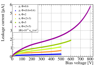
In Figure 14 the leakage current as a function of the applied bias voltage is summarised for the irradiated assemblies. All measurements were taken at an ambient temperature of to simulate as close as possible beam test environment temperatures where dry-ice cooling is employed. Again, the read-out chips were powered but not configured. The breakdown voltage of the irradiated sensors shifts to higher values and exceeds 500 V for all modules. Furthermore, the leakage currents are in agreement with expectations, showing increasing leakage currents with increasing fluences. Annealing effects are visible when comparing the module irradiated directly to a fluence of with the module irradiated in two steps, since for irradiation at JSI an annealing time of about 1.5 days is unavoidable due to handling after each irradiation step. The latter module could not be investigated further, since the FE-I3 read-out chip failed after the second irradiation and remounting onto the test card. The leakage currents for all modules are found to be A and thus again far below the operational limit of 300 A [1].
Assuming that all irradiated modules are fully depleted well below 450 V, it was verified that the damage factors are about A/cm, i. e. in agreement with theory predictions for the different target fluences and received periods of annealing [47].
3.2 Module Tuning
The module tuning and the charge collection measurements with radioactive sources were performed with the ATLAS USBPix read-out system [48]. The expected most probable value (MPV) for the charge induced by -electrons of the 90Sr decay chain is about 4.9 ke for the sensors with m [49, 50]. Therefore, the tuning is focussed on lowering the threshold as far as possible for each individual module. For the present FE-I3 read-out chip used in this R&D programme thresholds down to 3.2 ke are generally achievable. For some single chip modules even lower thresholds down to (2.0–2.5) ke have been reached. This signal to threshold ratio is challenging for modules employing the present read-out chip. However, results for the new ATLAS read-out chip FE-I4 show that it can be operated at thresholds as low as 1.6 ke [51], which is more than sufficient for the sensor thicknesses around 75 m presented here. An additional complication for the prototype modules is imposed by the not connected pixel cells for some of the modules. This implies that in the tuning two very different states of the read-out chip in adjacent regions have to be accommodated.
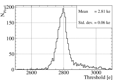
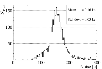
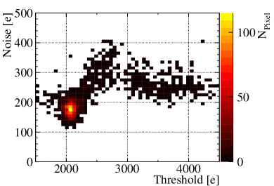
The threshold and noise distributions for a typical tuning are shown in Figure 15. The target threshold of 2.8 ke was reached for about 90 of the pixel cells with a standard deviation of 0.06 ke. The corresponding noise is 0.16 ke with a standard deviation of 0.03 ke over the module and thus not significantly different from the noise found for other n-in-n and n-in-p modules with thicknesses in the range (250-285) m [1, 14].
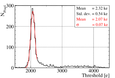
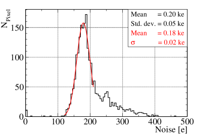
In Figure 16 the results of the tuning with the lowest achieved threshold and the corresponding noise among all modules before and after irradiation is depicted. It was achieved for the module irradiated to a fluence of . The mean threshold, shown in Figure 16, was tuned as low as ke with a standard deviation of ke across the module. The corresponding noise, shown in Figure 16, is ke with a standard deviation of ke across the module. The long tail of the distributions is mainly caused by pixel cells which could not be tuned to such low thresholds. The pixel-by-pixel correlation of threshold and noise, shown in Figure 16, demonstrates that the outliers in both distributions coincide. Since this is a known issue of the FE-I3 read-out chip, which is not planned to be used for future ATLAS upgrades, these outlier pixel cells are disregarded in the following. Fitting a Gaussian to the core of the distributions, for the tuning shown in Figures 16 and 16, the threshold lies at ke and the corresponding noise is ke.
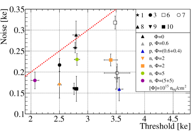
An overview of the threshold tuning and corresponding noise values of all modules before and after irradiation is given in Figure 17, where the lowest achieved thresholds and their corresponding noise values are given for each module. The uncertainties shown correspond to the standard deviation of threshold and noise, respectively. The average noise observed for all assemblies is ke. The slightly increased value with respect to currently used modules is due to the lower threshold target values and the influence of the not connected pixel cells. The effect of the not connected pixel cells is especially pronounced in the assemblies with the highest number of not connected cells, number 6 (open squares) and 7 (open circles). Nonetheless, an excellent threshold to noise ratio exceeding ten (red dotted line) in all but one case is achieved for assemblies before as well as after irradiation.
3.3 Charge Collection
Thin sensors show a higher CCE after irradiation, since the full depletion voltages are reduced, and higher electric fields are achieved when applying the same bias voltage. To investigate the charge collection, measurements using either photons from an 241Am source, or -electrons from a 90Sr source, were conducted. While for photons the internal trigger logic was used, for -electrons an external trigger was employed. Within uncertainties no significant difference in charge collection was found between the modules.
3.3.1 Radioactive Source Measurements
In Figure 18 the 241Am photon spectra obtained with a module biased at different bias voltages between 5 V and 55 V are depicted. Each histogram is normalised to its bin with the highest content. For a high resolution reference spectrum taken with a high purity Germanium detector please refer to [52, 53]. At 55 V the prominent 59 keV -line is measured at () ke (Gaussian fit not shown), which is in good agreement with the expected peak position of 16.4 ke, when taking into account the calibration bias of the FE-I3 read-out chip [54]. The first uncertainty denotes the one from the fit, and the second the systematic uncertainty stemming from the charge calibration of the read-out chip. The second prominent line in the spectrum at 26 keV is expected at 7.2 ke. However, due to the charge resolution it merges with the lines below, such that only the upper edge is appreciable, which lies between 6 ke and 7.5 ke.
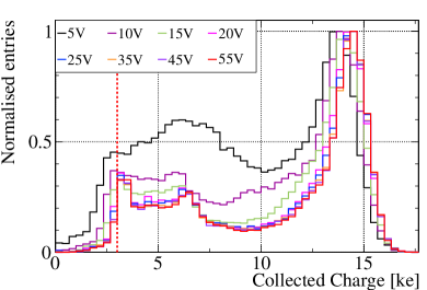
At lower bias voltages a fraction of the sensor volume does not contribute to the charge collection and thus the full amount of charge is only collected for events where the photo-electric process occurred in an already depleted region. For those events where it instead occurs in the not yet depleted part, only the fraction of the charges diffusing into the depleted volume can be measured. This leads to a broadening of the peaks and to a less defined spectrum. Due to the small thickness of the sensor, only the measurements below 15 V are significantly affected.
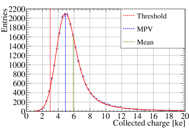
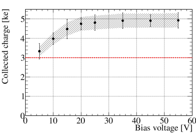
A charge distribution of a 90Sr measurement of a module operated at a bias voltage of 55 V is shown in Figure 19. The threshold in this measurement was tuned to 3.0 ke and is indicated by the red dotted line. Entries below threshold occur because the threshold corresponds to the 50 efficiency point. In addition indicated are the MPV (blue line) and the mean value (green line) of the collected charge. The measurement is well described by a convolution of a Landau distribution with a Gaussian. The fit, based on the statistical uncertainties of the data, was performed in the range 1–20 ke. The evolution of the resulting MPV of the collected charge as a function of the bias voltage is summarised in Figure 19. The uncertainty, shown as a band, is fully correlated from point to point and caused by the calibration uncertainty. Since the MPV of the collected charge is close to the threshold, the uncertainties arising from the fit are increased due to the deformation of the Landau distribution. They are indicated by the uncertainty bars. Full charge collection is reached at a bias voltage of V as determined by the intersection of two linear functions describing the different parts of the charge collection measurement.
This agrees well with the infra-red laser measurements on strips from the same production. For the module shown the charge saturates at ke and thus is in good agreement with the expectations for a sensor with m.
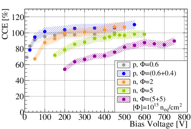
Aiming for usage at the expected HL-LHC environment, a high CCE at high irradiation levels is of utmost importance. The measured values of this parameter are summarised for all irradiated modules as a function of the applied bias voltage and for different received fluences (colour) in Figure 20. Since the uncertainties stemming from the charge calibration before and after irradiation are highly correlated they almost completely cancel, when investigating the ratio. Still, as a conservative estimate a 5 uncertainty is assigned to the ratio. As expected from the strip measurements [15], within the assessable voltage range, a saturation is found up to the highest fluences. The onset of the saturation increases with fluence, but lies at comparably low voltages for all fluences, i. e. below 500 V. These low bias voltages, in combination with the fact that all modules saturate within uncertainties to a CCE of 100 up to a received fluence of and to 90 at a received fluence of , allows to operate them in a restricted bias voltage range over the entire life-time of an experiment. This leads to looser requirements on the read-out electronics.
For comparison in Figure 20 the results obtained from infra-red laser measurements on strip sensors from the same production are depicted together with the results obtained with the pixel modules for the two highest received fluences [15]. For this figure the infra-red laser measurements were renormalised globally to achieve comparable scales. For the measurement at an excellent agreement is found over the entire range. At the higher fluence slight deviations at low and high applied bias voltages are observed, which are most likely caused by the different annealing history of the structures, given the two step irradiation procedure for the pixel module. However, considering the use of a single scaling factor over the entire range, a good agreement is achieved.
3.4 Cluster Size
The cluster size and hit efficiency were determined with test beam data obtained with 120 GeV pions at the CERN SPS. The position within a given pixel assembly under test where the particle traverses the assembly is determined from external information provided by the EUDET beam telescope [55]. Analysing the signals from the pixels around this position the cluster size and the hit efficiency can be determined.
For thinner sensors the spatial resolution is expected to differ from the one observed for thick sensors given the different cluster size abundances. However, when comparing the resolution on events with a specific cluster size between different thicknesses no difference is expected. In any case, lower cluster sizes lead to a reduced occupancy.
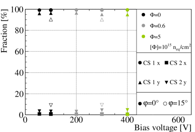
The low absolute collected charge to threshold ratio is reflected in the smaller abundances of higher multiplicity clusters. In Figure 21 a summary of the cluster size as a function of the bias voltage for different received fluences (colour), spatial coordinates (symbol style), and particle incidence angles (closed/open symbols) is given. The uncertainties are calculated according to [56] and are smaller than the symbol sizes. In the direction of the short pixel pitch only about 5 of two-hit clusters are observed for perpendicular incidence. If the modules are tilted by , as it is foreseen for the IBL, about 10 of the clusters in are composed of two hits. As expected from the CCE measurements, no difference is found before and after irradiation, provided that the applied bias voltage is around or above the value corresponding to the charge saturation.
3.5 Hit Efficiency
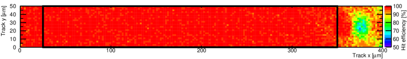
Besides the resolution, the tracking efficiency of the pixel detector is the key figure of merit. For a high tracking efficiency, a high hit efficiency of the pixel assemblies is mandatory. The latter is mainly driven by the ratio between collected charge and threshold. Consequently, for thinner sensors the lowest possible threshold is desirable as discussed before. This criterion is especially challenging since the difference between the mean threshold and the MPV of the collected charge is so small that a part of the distribution lies below threshold, as shown for example in Figure 19. Since the threshold corresponds to an efficiency of 50 for the electronic circuit of the pixel cell this considerably diminishes the overall hit efficiency. In Figure 22 the mean hit efficiency as a function of the impact point predicted by the beam telescope is depicted for a bias voltage of 100 V. For this measurement, the thresholds were tuned to 2800 e.
The impact of the comparably high threshold is most pronounced in the area of the punch-through bias structure, and in the corner regions, where it leads to a loss of hit efficiency due to the sharing among several pixels. Anyhow, both effects are most pronounced for perpendicular impinging particles, occurring only for the very central part of a high energy physics experiment. Therefore, the quoted hit efficiency has to be understood as a lower bound. The overall hit efficiency is found to be . If just the central region, indicated by the box in Figure 22, is considered, the hit efficiency rises to . Although this hit efficiency is still high when taking into account the challenging charge to threshold ratio, it clearly shows that the present ATLAS read-out chip in combination with sensors of 75 m is not optimal for tracking purposes. Notwithstanding the high CCE, the situation stays challenging after irradiation and thus a discussion of the hit efficiencies is not sensible and omitted here.
The lower minimal thresholds offered by the FE-I4 read-out chip improves the charge to threshold ratio, and might allow to use sensors as thin as 75 m. Nonetheless, already sensors as thin as 150 m exhibit a very good CCE after irradiation and are operable at comparably low bias voltages [13].
4 Conclusions
Mechanical and electrical results obtained with SLID interconnected structures from an R&D campaign towards a new pixel module were discussed. The investigated concept is based on several new technologies, namely n-in-p sensors, thin sensors, slim edges with or without active edges, and 3D-integration incorporating SLID interconnections as well as ICVs.
The 3D-integration is foreseen in the module concept to achieve compact module. The SLID interconnection technique by EMFT was qualified for use on pixel sensors by verifying the effectiveness of the TiW diffusion barrier and determining the needed vertical and horizontal alignment precision. Especially, it was shown that deliberate height mismatches of up to 1 m are not detrimental for the connection efficiency. First prototype modules employing the ATLAS FE-I3 read-out chip and 75 m thick sensors were built. It was shown that SLID interconnections have a stability and durability similar to other interconnection technologies used. Furthermore, all pixel cells were interconnected for assemblies where the underlying BCB passivation layer was fully opened in correspondence to the SLID interconnections. An SF6 plasma descum process will guarantee that interconnections the BCB passivation layer are opened sufficiently everywhere in future. Also at the moment new tools and processes are installed and implemented at EMFT to further improve on the alignment precision, which will allow for even smaller pitches.
For the prototype modules the CCE and the absolute collected charge were investigated systematically as functions of the received fluence and the applied bias voltage. The results were compared to results obtained with strip sensors from the same production. It was shown that after an irradiation to a received fluence of , assemblies with a thickness of m saturate at a CCE of 90 to 100. For an application within an experiment, in addition to the CCE also the absolute charge and its relation to the threshold of the read-out chip has to be taken into account. Although, with the low thresholds possible with the new FE-I4 read-out chip using a sensor thickness down to about 75 m seems feasible, the absolute charge measurement indicates that a somewhat larger charge would be preferable to retain a good signal to threshold ratio up to the highest fluences expected. Anyhow, other factors like the lowered occupancy of thinner detectors might render thinner sensors still to be the better choice. Furthermore, the requirements on high voltage stability are relaxed for thinner sensors since thinner sensors exhibit a high CCE already at moderate bias voltages. In conclusion, the good properties of the sensors and modules presented here make them well suited for use in ATLAS when operating at the HL-LHC.
5 Acknowledgements
This work has been partially performed in the framework of the CERN RD50 Collaboration. The authors thank A. Dierlamm (KIT), and V. Cindro and I. Mandić (Jožef-Stefan-Institut) for the sensor irradiation. Part of the irradiation programme was supported by the Initiative and Networking Fund of the Helmholtz Association, contract HA-101 (”Physics at the Terascale”). Another part of the irradiation and the beam test measurements leading to these results has received funding from the European Commission under the FP7 Research Infrastructures project AIDA, grant agreement no. 262025. Beam test measurements were conducted within the PPS beam test group comprised by: S. Altenheiner, M. Backhaus, M. Bomben, D. Forshaw, Ch. Gallrapp, M. George, J. Idarraga, J. Janssen, J. Jentzsch, T. Lapsien, A. La Rosa, A. Macchiolo, G. Marchiori, R. Nagai, C. Nellist, I. Rubinskiy, A. Rummler, G. Troska, Y. Unno, P. Weigell, J. Weingarten.
References
- [1] G. Aad et al., ATLAS pixel detector electronics and sensors, JINST 3, (2008), P07007.
- [2] I. Peric et al., The FEI3 readout chip for the ATLAS pixel detector, Nucl. Instr. and Meth. A565, (2010), 178.
- [3] T. Fritzsch et al., Cost effective flip chip assembly and interconnection technologies for large area pixel sensor applications, Nucl. Instr. and Meth. A650, (2011), 189.
- [4] L. Rossi et al., High Luminosity Large Hadron Collider: A Description for the European Strategy Preparatory Group, CERN, (2012), CERN-ATS-2012-236.
- [5] M. Capeans et al., ATLAS Insertable B-Layer Technical Design Report, CERN, (2010), CERN-LHCC-2010-013.
- [6] M. Benoit, Étude des détecteurs planaires pixels durcis aux radiations pour la mise à jour du d’etecteur de vertex d’ATLAS, PhD thesis, (2011), University Paris Sud - Paris XI.
- [7] T. Wittig, Design and Quality Control of Planar ATLAS IBL Sensors Based on Slim Edge Studies, PhD thesis, (2013), Technical University Dortmund.
- [8] ATLAS IBL Collaboration, Prototype ATLAS IBL Modules using the FE-I4A Front-End Readout Chip, JINST 7, (2012), P11010.
- [9] M. Garcia-Sciveres et al., The FE-I4 pixel readout integrated circuit, Nucl. Instr. and Meth. A636 Supplement, (2011), S155.
- [10] ATLAS Collaboration, Letter of Intent for the Phase-II Upgrade of the ATLAS Experiment, CERN, (2012), CERN-2012-022 LHCC-I-023, https://cds.cern.ch/record/1502664.
- [11] L. Andricek et al., Processing of ultra-thin silicon sensors for future e+e- linear collider experiments, IEEE Trans. Nucl. Sci. 51, (2004), 1117.
- [12] Fraunhofer Einrichtung für Modulare Festkörper-Technologie, http://www.emft.fraunhofer.de/.
- [13] S. Terzo et al., Heavily irradiated n-in-p thin planar pixel sensors with and without active edges, Proceedings of the iWoRID 2013 Conference, JINST 9 (2014), C05023.
- [14] C. Gallrapp et al., Performance of novel silicon n-in-p planar pixel sensors, Nucl. Instr. and Meth. A679, (2012), 29.
- [15] P. Weigell, Investigation of properties of novel silicon pixel assemblies employing thin n-in-p sensors and 3D-integration, PhD Thesis, (2013), Technical University München, MPP-2013-5, CERN-THESIS-2012-229.
- [16] G. Casse et al., Enhanced efficiency of segmented silicon detectors of different thicknesses after proton irradiations up to neq/cm2, Nucl. Instr. and Meth. A624, (2010), 401.
- [17] I. Mandić et al., Observation of full charge collection efficiency in heavily irradiated n+p strip detectors irradiated up to neq/cm2, Nucl. Instr. and Meth. A612, (2010), 474.
- [18] A. Macchiolo et al., Thin n-in-p pixel sensors and the SLID-ICV vertical integration technology for the ATLAS upgrade at HL-LHC, Nucl. Instr. and Meth. A731 (2013) 210.
- [19] A. Macchiolo et al., SLID-ICV Vertical Integration Technology for the ATLAS Pixel Upgrades, Phys. Proc. 37, (2012), 1009.
- [20] P. Weigell et al., Characterization of Thin Pixel Sensor Modules Interconnected with SLID Technology Irradiated to a Fluence of 2 neq/cm2, JINST 6, (2011), C12049.
- [21] A. Macchiolo et al., Performance of thin pixel sensors irradiated up to a fluence of neq/cm2 and development of a new interconnection technology for the upgrade of the ATLAS pixel system, Nucl. Instr. and Meth. A650, (2011), 145.
- [22] M. Beimforde et al., A module concept for the upgrades of the ATLAS pixel system using the novel SLID-ICV vertical integration technology, JINST 5, (2010), C12025.
- [23] M. Beimforde, Development of thin sensors and a novel interconnection technology for the upgrade of the ATLAS pixel system, PhD Thesis, (2010), Technical University München, MPP-2010-115, CERN-THESIS-2010-280.
- [24] L. Blanquart et al., FE-I2: a front-end readout chip designed in a commercial 0.25-m process for the ATLAS pixel detector at LHC, IEEE Trans. Nucl. Sci. 51, (2004), 1358.
- [25] T. Stockmanns, Multi-Chip-Modul-Entwicklung für den ATLAS-Pixeldetektor, PhD Thesis, (2004), Bonn University.
- [26] P. Weigell et al., Characterization and performance of silicon n-in-p pixel detectors for the ATLAS upgrades, Nucl. Instr. and Meth. A658, (2011), 36.
- [27] L. Bernstein et al., Applications of Solid-Liquid Inderdiffusion (SLID) Bonding in integrated-Circuit Fabrication, Trans. Met. Soc. AIME 236m, (1966), 405.
- [28] L. Bernstein, Semiconductor brazing by the solid-liquid-inter-diffusion (SLID) process, in: ECS Meeting, San Francisco, (1965), 319.
- [29] A. Klumpp, Bonding with Intermetallic Compounds in P. Garrou et al., Handbook of 3D Integration: Technology and Applications of 3D Integrated Circuits, Wiley-VCH, Weinheim(Germany), (2008), 261
- [30] H. Hübner et al., Face-to-Face Chip Integration with Full Metal Interface, in B. Melnick et al., Advanced Metallization Conference Proceedings XVIII, (2002), 53.
- [31] G. Deptuch et al., 3D Technologies for Large Area Trackers, Whitepaper Submitted to Snowmass 2013, http://arxiv.org/pdf/1307.4301.pdf
- [32] S. Joblot et al., Copper pillar interconnect capability for mmwave applications in 3D integration technologies, Microelectronic Engineering 107, (2013), 72.
- [33] Leti, http://http://www-leti.cea.fr.
- [34] Keithley Instruments Inc, http://www.keithley.com/.
- [35] A.A. Istratov and E.R. Weber, Physics of Copper in Silicon, Journal of the Electrochemical Society 149 (1), (2002), G21.
- [36] ATLAS Collaboration, Pixel Detector Technical Design Report, CERN, (1998), CERN-LHCC-98-013.
- [37] A. Klumpp, EMFT, private communication.
- [38] Fraunhofer Institut für Zuverlässigkeit und Mikrointegration, http://www.izm.fraunhofer.de/.
- [39] T. Go, Bonding of aligned conductive bumps on adjacent surfaces, US Patent 4912545, (1987).
- [40] Ch. Broennimann et al., Development of an Indium bump bond process for silicon pixel detectors at PSI, Nucl. Instr. and Meth. A565, (2006), 303.
- [41] J. Eldring et al., Flip Chip Attach of Silicon and GaAs Fine Pitch Devices as well as Inner Lead TAB Attach Using Ball-bump Technology, Microelectron Int. 11, (1994), 20.
- [42] Ch. Broennimann et al., The PILATUS 1M detector, J. Synch. Rad. 13, (2006), 120.
- [43] L. Cheah et al., Gold to gold thermosonic flip-chip bonding, SPIE Proc. Series 4428, (2001), 165.
- [44] A. Dierlamm, Untersuchungen zur Strahlenhärte von Siliziumsensoren, PhD Thesis, (2003), Karlsruhe University, IEKP-KA/2003-23.
- [45] A. Furgeri, Qualitätskontrolle und Bestrahlungsstudien an CMS Siliziumstreifensensoren, PhD Thesis, (2006), Karlsruhe University, IEKP-KA/2005-1.
- [46] L. Snoj et al., Computational analysis of irradiation facilities at the JSI TRIGA reactor, Appl. Rad. Iso. 70, (2012), 483.
- [47] M. Moll, Radiation Damage in Silicon Particle Detectors, PhD Thesis, (1999), Hamburg University.
- [48] USB based readout system for ATLAS FE-I3 and FE-I4, http://icwiki.physik.uni-bonn.de/twiki/bin/view/Systems/UsbPix.
- [49] H. Bichsel et al., Passage of Particles through matter, J. Phys. G 637, (2010), 285.
- [50] H. Bichsel, Straggling in thin silicon detectors, Rev. Mod. Phys. 60, (1988), 663.
- [51] M. Backhaus, Characterization of new hybrid pixel module concepts for the ATLAS Insertable B-Layer upgrade, JINST 7, (2012), C01050.
- [52] R. Gehrke et al., Radioactinide additions to the electronic Gamma-ray Spectrum Catalogue, J. Rad. Nucl. Chem. 248, (2001), 417.
- [53] Ray Spectrometry Center, Gamma-Ray spectrum catalogue Idaho National Engineering & Environmental Laboratory, (2001).
- [54] J. Große-Knetter, Vertex Measurement at a Hadron Collider, The ATLAS Pixel Detector, Habilitation thesis, Bonn University, (2008), BONN-IR-2008-04.
- [55] I. Rubinskiy, An EUDET/AIDA Pixel Beam Telescope for Detector Development, Phys. Proc. 37, (2012), 923.
- [56] M. Paterno, Calculating Efficiencies and Their Uncertainties, FERMILAB, (2004), FERMILAB-TM-2286-CD.