Development of active edge pixel sensors and four-side buttable modules using vertical integration technologies
Abstract
We present an R&D activity focused on the development of novel modules for the upgrade of the ATLAS pixel system at the High Luminosity LHC (HL-LHC). The modules consist of n-in-p pixel sensors, 100 or 200 m thick, produced at VTT (Finland) with an active edge technology, which considerably reduces the dead area at the periphery of the device. The sensors are interconnected with solder bump-bonding to the ATLAS FE-I3 and FE-I4 read-out chips, and characterized with radioactive sources and beam tests at the CERN-SPS and DESY. The results of these measurements will be discussed for devices before and after irradiation up to a fluence of . We will also report on the R&D activity to obtain Inter Chip Vias (ICVs) on the ATLAS read-out chip in collaboration with the Fraunhofer Institute EMFT. This step is meant to prove the feasibility of the signal transport to the newly created readout pads on the backside of the chips allowing for four side buttable devices without the presently used cantilever for wire bonding. The read-out chips with ICVs will be interconnected to thin pixel sensors, 75 m and 150 m thick, with the Solid Liquid Interdiffusion (SLID) technology, which is an alternative to the standard solder bump-bonding.
keywords:
Pixel detector , n-in-p , ATLAS , HL-LHC , Active edges , Vertical Integration1 Introduction
The ATLAS pixel system will undergo around the years 2022-2023 a complete replacement to cope with the higher detector occupancy and radiation doses foreseen in the High Luminosity phase of the LHC (HL-LHC) [1]. The possibility of employing thin pixel detectors is very attractive for the inner layers of the upgraded ATLAS pixel system, given the reduced material usage that helps minimizing the multiple scattering experienced by charged particles. Other advantages offered by thin pixels are the good charge collection efficiency after irradiation, thanks to the higher electric field that can be established in the silicon bulk with respect to thicker devices, and the possibility of reducing the number of clusters with more than two hit pixels, that are detrimental for the position resolution and the detector occupancy. This is particularly important for the inner layers, where more particles traverse the pixel modules at high pseudo-rapidity (). For example, at the maximum value of 2.5 covered by the ATLAS Insertable B-Layer [2], 250 m thick sensors, with 250 m pitch along the beam direction, yield a mean cluster size of 7.1, while 150 m thick sensors a mean cluster size of 4.6, as reported in [3].
The performance of 75 and 150 m thin n-in-p pixel sensors produced at the Semiconductor Laboratory of the Max-Planck Society are discussed in [4]. In particular, it has been shown, that a charge collection efficiency (CCE) of (909)% was obtained at a bias voltage of 750 V after irradiation at a fluence of for the 75 m thin sensors interconnected to FE-I3 chips [5]. In addition, it has also been reported in [4] that the 150 m thin sensors, interconnected to FE-I4 chips [6], after being irradiated at a fluence of , yield hit efficiencies of (96.50.3)% at 400V and (96.90.3)% at 500V, for perpendicular beam incidence.
2 Active edge pixels
An additional requirement to instrument the inner pixel layers is the reduction of the module inactive area due to space constraints that do not allow for overlapping the sensors along the beam direction. Different approaches have been followed to achieve this goal for planar pixel detectors, as documented in [7]. We report here on the results obtained with Deep Reactive Ion Etching (DRIE), to achieve trenches around the sensors, which allow for a doping of the sensor sides. This technology has been used for a multi project production of active edge n-in-p pixel sensors at VTT on 6” wafers. These devices were bump-bonded at VTT to FE-I3 and FE-I4 chips, and the results of the first electrical characterization have been reported in [4]. The bulk material, where not explicitely otherwise indicated, is Float Zone (FZ) p-type silicon, with an initial resistivity of 10 k cm. The fabrication of thin sensors at VTT exploits the use of a handle wafer as mechanical support during the grinding phase. Trenches are created at the sensor border by wet etching, and then activated by means of four-quadrant ion implantations with boron [8, 9]. In the pixel production discussed in this paper, sensors were manufactered with a thickness of 100 or 200 m. At the end of the sensor production the handle wafer is removed before the interconnection via solder bump-bonding to the chips. An homogeneous p-spray method, with an uniform low-dose boron implantation, has been used to to achieve the inter-pixel isolation.
Two versions of reduced edge design have been implemented, as shown in Fig.1. The first one is characterized by one guard and one bias ring, with the latter connected to the pixel punch-through structures, allowing for testability before interconnection. In this case the edge width, dedge, defined as the distance between the end of the last pixel implant and the trench, is equal to 125 m. The second, more aggressive design, implemented only for FE-I3 sensors, foresees one floating guard-ring and dedge=50 m.
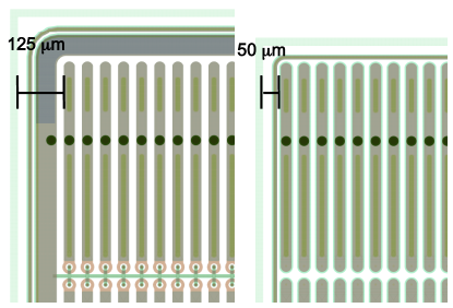
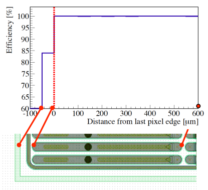
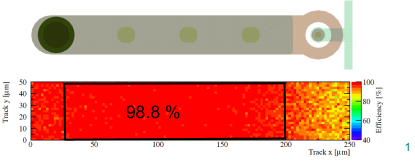
The absence of the bias ring also leads to the omission of the bias dot and bias rail structures. These devices, before irradiation, have been characterized in a beam test at the CERN-SPS with 120 GeV pions. The global module efficiency and the hit efficiency at the sensor edge have been extracted. The FE-I3 and FE-I4 modules yield a global efficiency of % and % respectively, at a bias voltage of 20 V. The dominant source of the uncertainty for these measurements is systematic, and it has been evaluated as described in [10]. Fig.2 shows the hit efficiency obtained over the edge pixel column, as a function of the distance from the end point of the pixel implant, for the sensor design with only a guard-ring. A value of % is found over the entire lenght of the pixel implantation, while in the 50 m wide edge, a hit efficiency of (84)%, where the uncertainty is statistically dominated, demonstrates that the sensor is still active also in this region. A detailed analysis of the edge efficiency for different geometries can be found in [3].
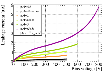
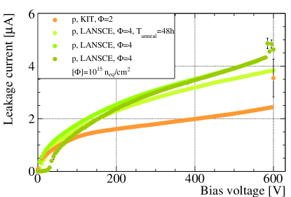
Some samples of the active edge pixel devices were irradiated at different fluences. A summary of the leakage currents measured for these sensors is presented in Fig.3. As expected, the current values scale according to the thickness and the fluence received. The breakdown voltages, indicated by the rightmost data point, are larger than before irradiation [4], with the highest value of 350 V corresponding to the sample irradiated to the highest fluence achieved so far of . However, the breakdown voltages for these samples are generally lower than those measured for thin n-in-p pixels devices of other productions with a guard-ring structure, irradiated at the same fluences. For comparison the IV curves of 75 m thin detectors with 1 mm wide guard ring structures and of 150 m detectors, with a 450 m wide structures, are reported in Fig.4 and Fig.5 [11].
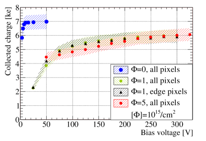
All the measurements of charge collection described in this paper were performed by using the ATLAS USBPix read-out system [12]. The modules after irradiation were tested at an environmental temperature of T=-50∘C inside a climate chamber to reproduce the conditions during the test-beam where the cooling is realized with dry ice. The Time over Threshold (ToT) to charge calibration was corrected by using measurements with 109Cd and 241Am radioactive sources. A residual systematic error of 10% was assigned to the charge values extracted in runs with a 90Sr source. A VTT FE-I3 pixel module with an edge width of 125 m has been irradiated at the Karlsruhe Institute of Technology (KIT) with 25 MeV protons at a fluence of , and tested with a 90Sr source up to a bias voltage of 300 V. Fig.6 shows that the collected charge in the edge pixels (black curve) is comparable to to the charge collected in the inner part of the module (green curve), similarly to what was observed before irradiation [4]. At Vbias=300 V, the collected charge is (869)% of the value collected before irradiation. The same module was afterwards irradiated with reactor neutrons at the Jožef Stefan Institute (JSI) in Slovenia at a fluence of , for a total received fluence of . The charge collection properties at this higher irradiation fluence did not degrade further and the corresponding results are reported as the red curve in Fig. 6.
.
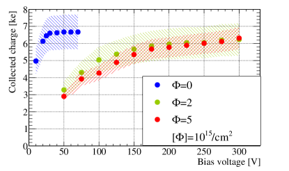
A confirmation of the good charge collection properties of these thin detectors was achieved with a FE-I4 sensor, also 100 m thick and with a 125 m wide edge. In this case the bulk material consists of MCz silicon, with orientation 100 and an initial resistivity of 2 K cm. The module was irradiated at KIT with 25 MeV protons in two successive steps first at a fluence of and then at a total fluence of . The charge collection with a 90Sr source is compared before and after irradiation in Fig.7. At the fluence of , with 300V of bias voltage, (919)% of the pre-irradiation charge is achieved.
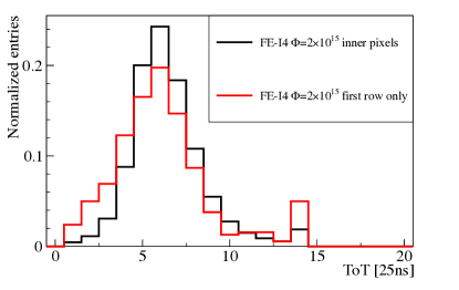
The Landau distributions of the collected charge for the internal and the edge pixels, at a bias voltage of 300 V and at a fluence of , are presented in Fig.8. The measurement was performed using a 90Sr source. Also for this device the edge pixels show a comparable charge collection performance with respect to the internal ones.
These irradiated detectors were tested with a 4 GeV electron beam at DESY, using the EUDET telescope for track reconstruction [10]. Hit efficiencies, as a function of the bias voltage, were derived for the pixel modules, as shown in Fig.9.
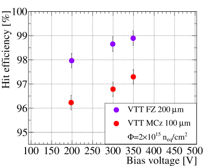
Fig.10 shows the values of the hit efficiency of the 100 m thick sensor for all tracks projected into one single pixel cell, as a function of the impact point predicted by the beam telescope. The lower global efficiency of this module was traced back to the pixel area corresponding to the punch-through structure and bias rail. The contours of the low efficiency region are smeared due to the effect of the not optimal telescope pointing resolution for this particular setup, estimated to be 27 m. This value has been obtained from the residual distribution of single hit clusters after disentangling the contribution of the pixel intrinsic digital resolution. The module with the 200 m thick sensor, measured in the same conditions, does not show instead a decrease of the hit efficiency in the area of the punch-through structure and bias rail, resulting in an overall higher hit efficiency. The partial loss of efficiency in the pixel biasing structure has been observed also for other thin pixel production and for pixel sensors of standard thickness at higher fluences [3, 11, 13].
Parallel activities on the production of active edge planar pixel sensors are pursued also by other groups, for example with the fabrication at FBK of FE-I4 compatible sensors with a similar approach to the one followed at VTT, with the main difference being in the technology adopted for the trench doping [14].
3 Vertical Integration Technologies
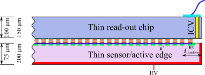
Active edge pixels represent a successfull technology to reduce the dead area of tracking detectors but to obtain modules that can be tiled along all four sides, also the read-out chips have to be redesigned to eliminate or strongly diminish the inactive regions. Vertical integration technologies can be used to solve these problems, applying Inter Chip Vias (ICV) to transport the signals from the front- to the back-side. In this way hybrid pixel modules could be built with chips without the cantilever where the wirebond pads are normally located. Fig11 shows the concept of an hybrid pixel modules, assembled with active edge pixels and the read-out chip with ICVs.
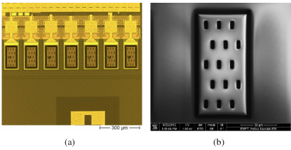
A project about the application of vertical integration technologies to tracking detectors was initiated to demonstrate the use of ICVs together with the Solid Liquid Interdiffusion (SLID) interconnection, studied as a possible alternative to bump-bonding. These two technologies have been developed by the Fraunhofer Institute EMFT and the processing described in the following has been performed in their clean-room facilities. SLID is based on the formation of Cu-Sn alloys where the interconnection takes place at temperatures significantly lower than the ones that the alloy can withstand [15]. Therefore it allows for stacking of different interconnected chip and sensor layers without destroying the pre-existing bonds. The SLID bond pads can have an arbitrary shape and size, with the only constraint that its dimensions exceed 5 m by 5 m. In previous runs, a successfull SLID interconnection of FE-I3 chips to pixel sensors with 75 m thickness has been demonstrated in the chip to wafer approach [4]. In a successive step of this R&D program, FE-I3 chips are dedicated to the assembly of a demonstrator module for ICVs, still using the SLID interconnection to pixel sensors with 75 m and 150 m active thickness. Since this read-out chip was not designed for the usage with ICVs, these have been etched at the location of the original wire-bonding pads where the volume below is not filled with logic blocks. Several redundant ICVs were etched into each wire-bonding pad as illustrated in Fig.12(a). To insulate the volumes of neighbouring wire-bonding pads against each other, an additional encircling trench is etched. An optimization of the process on test wafers has resulted in choosing the cross-section of the ICVs to be 310 m2. The ICVs have been first etched using DRIE with columns reaching a depth of 60 m. Subsequentely they are isolated with Chemical Vapor Deposition (CVD) of silicon dioxide and filled with tungsten CVD to create the conductive pin between front and back-side [15]. The FE-I3 chip wafer has been then thinned to 60 m of thickness after having attached a support wafer on the front-side, in such a way that the ICVs are exposed, as shown in Fig.12(b).
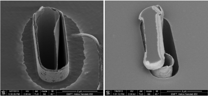
A removal of the back-side isolation dioxide has finally been performed, with the recess of the CVD silicon dioxide at the bottom of the ICV to create the contact to the underlying tungsten. At this stage it has been observed that the tungsten deposition has not been successfull and the ICVs are hollow. In Fig.13 the ICVs after recess of the CVD silicon dioxide are shown. The walls of the ICVs are coated only with a 60 nm thick layer of TiN, deposited before the tungsten as an adhesion layer. The filling of ICVs with tungsten has been previously demonstrated by EMFT with this Vias cross-section in other productions and with test-wafers. The aging of the tungsten gas used during the Chemical Vapor Deposition has been identified as a possible cause of this failure.
Still the interconnection of these chips to the FE-I3 compatible sensors with SLID is planned to investigate the feasibility of handling such thin structures without affecting their mechanical and electrical properties. The wire bonding of the modules is still possible thanks to a fan-out structure foreseen as back-up solution on the sensor side. A second project to create ICVs on the FE-I4 chips has been recently started. For this R&D activity a new ICV process has to be developed, because the etching needs to be performed starting from the back-side, contrary to the FE-I3 case, given the presence of many metal layers below the wire bonding pads. The ICVs will contact the first metal layer of the chip, internally connected in the fan-out structure to the last metal on top of the wire bonding pad. The target final thickness of the FE-I4 chips is in the range of (100-150) m.
4 Conclusions
Active edge planar pixel sensors, 100 and 200 m thick, interconnected to FE-I3 and FE-I4 chips, have been characterized before and after irradiation up to a fluence of . Good charge collection properties and hit efficiencies in beam tests with 4 GeV electrons at DESY have been obtained. Given their narrow inactive region and their reduced thickness, they represent good candidates to instrument the inner layers of the upgraded ATLAS pixel detector at HL-LHC. An R&D activity to obtain Inter Chip Vias (ICVs) on the ATLAS read-out chip has started in collaboration with the Fraunhofer Institute EMFT. This step is meant to prove the feasibility of the signal transport to the newly created readout pads on the backside of the chips allowing for four side buttable devices without the presently used cantilever for wire bonding. The ICVs are planned to be used in combination with the SLID interconnection in a new run to build a demonstrator module assembled with FE-I4 chips and thin n-in-p planar pixel sensors.
5 Acknowledgements
This work has been partially performed in the framework of the CERN RD50 Collaboration. The authors thank V. Cindro for the irradiation at JSI, A. Dierlamm for the irradiation at KIT and S. Seidel (University of New Mexico) for the irradiations at LANSCE. The irradiations at KIT were supported by the Initiative and Networking Fund of the Helmholtz Association, contract HA-101 (”Physics at the Terascale”). The irradiation at JSI and the beam-tests have received funding from the European Commission under the FP7 Research Infrastructures project AIDA, grant agreement no. 262025. Beam test measurements were conducted within the PPS beam test group comprised by: M. Backhaus, M. Benoit, M. Bomben, G. Calderini, K. Dette, M. Ellenburg, D. Forshaw, Ch. Gallrapp, M. George, S. Gibson, S. Grinstein, J. Idarraga, J. Janssen, Z. Janoska, J. Jentzsch, O. Jinnouchi, R. Klingenberg, T. Kishida, A. Kravchenko, T. Kubota, T. Lapsien, A. La Rosa, V. Libov, A. Macchiolo, G. Marchiori, D. Muenstermann, R. Nagai, C. Nellist, G. Piacquadio, R. Plumer, B. Rastic, I. Rubinskiy, A. Rummler, Y. Takubo, S. Terzo, K. Toms, G. Troska, S. Tsiskaridtze, I. Tsurin, Y. Unno, R. Wang, P. Weigell, J. Weingarten and T. Wittig.
References
- [1] O. Brüning, L. Rossi, et al., ”High-Luminosity Large Hadron Collider; A description for the European Strategy Preparatory Group”, Tech. Rep. CERN-ATS-2012-236, CERN (Geneva, 2012).
- [2] M. Capeans et al., “ATLAS Insertable B-Layer Technical Design Report”, CERN-LHCC-2010-013, Geneva Sep. 2010.
- [3] S. Terzo et al., ”Heavily irradiated n-in-p thin planar pixel sensors with and without active edges”, Proceedings of the iWoRID 2013 Conference, to be published in JINST.
- [4] A. Macchiolo et al., ”Thin n-in-p pixel sensors and the SLID-ICV vertical integration technology for the ATLAS upgrade at the HL-LHC”, Proceedings for Pixel 2012 Conference, Nucl. Instr. and Meth. A, in press, http://arxiv.org/abs/1210.7933
- [5] I. Peric et al., ”The FEI3 readout chip for the ATLAS pixel detector”, Nucl. Instr. and Meth. A565 (2006) 178.
- [6] M. Garcia-Sciveres et al., ”The FE-I4 pixel readout integrated circuit”, Nucl. Instr. and Meth. A636, No. 1 Supplement (2011), S155.
- [7] Philipp Weigell on behalf of the ATLAS Planar Pixel Sensors R&D Project, ”Recent results of the ATLAS upgrade planar pixel sensors R&D project”, Proceedings for Pixel 2012 Conference, Nucl. Instr. and Meth. A, in press, http://arxiv.org/abs/1210.7661v2.
- [8] S. Eranen et al., ”3D processing on 6 in. high resistive SOI wafers: Fabrication of edgeless strip and pixel detectors”, Nucl. Instr. and Meth. A607 (2009) 85.
- [9] X Wu et al., ”Recent advances in processing and characterization of edgeless detectors”, JINST 7 (2012), http://dx.doi.org/10.1088/1748-0221/7/02/C02001.
- [10] J.Weingarten, et al., ”Planar Pixel Sensors for the ATLAS Upgrade: Beam Tests results”, accepted by JINST, http://arxiv.org/abs/arXiv:1204.1266.
- [11] P.Weigell, ”Investigation of Properties of Novel Silicon Pixel Assemblies Employing Thin n-in-p Sensors and 3D-Integration”, PhD Thesis, (2013), TU Mu¨nchen CERN-THESIS-2012-229.
- [12] http://icwiki.physik.uni-bonn.de/twiki/bin/view/Systems/UsbPix#Hardware
- [13] ATLAS IBL Collaboration, ”Prototype ATLAS IBL Modules using the FEI4A Front-End Readout Chip”, JINST 7, (2012), P11010.
- [14] M. Bomben et al., Nucl. Instr. and Meth. A 712 (2013) 41.
- [15] A. Klumpp et al., ”3D-Integration of Silicon Devices: A Key Technology for Sophisticated Products” in ”Design, Automation Test in Europe Conference Exhibition”, pp. 1678-1683, 2010.