Potential fluctuations in graphene due to correlated charged impurities in substrate
Abstract
We evaluate the autocorrelation function of the electrostatic potential in doped graphene due to nearby charged impurities. The screening of those impurities is described by a combination of the polarization function for graphene in random phase approximation with the electrostatic Green’s function of the surrounding dielectrics. Using the hard-disk model for a two-dimensional distribution of impurities, we show that large correlation lengths between impurities can give rise to anti-correlation in the electrostatic potential, in agreement with recent experiments.
pacs:
73.22.Pr, 72.80.Vp, 81.05.ueMany future applications of graphene in electronics, photonics,Avouris_2012 and biochemical sensingAllen_2010 are based on specific properties of the low-energy excitations of its electrons described as Dirac fermions. Being an all-surface material enables efficient tuning of the equilibrium charge carrier density in graphene by applying an electric potential to external gates or by doping due to controlled adsorption of atoms or molecules, but it also renders graphene extremely sensitive to the chemical and structural imperfections in the surrounding materials. For example, charged impurities are ubiquitous in SiO2 that is commonly used for supporting exfoliated graphene, Ishigami_2007 ; Romero_2008 and are found to give rise to spatial variation of the Dirac point across graphene resulting in a quite inhomogeneous distribution of its charge carriers.Martin_2008 ; Zhang_2009 ; Deshpande_2009 ; Deshpande_2011 ; Gomez_2012 When the Fermi energy of graphene is tuned to sit at the average position of its Dirac point, such inhomogeneity in charge carriers gives rise to a system of electron-holes puddles that is responsible for the famed conductivity minimum in a nominally neutral graphene. Tan_2007 ; PNAS_2007 ; Sarma_2011 On the other hand, even in the cases when the average equilibrium areal number density of charge carriers is relatively large, as is the case in graphene on SiO2,Ishigami_2007 ; Romero_2008 the fluctuations in charge carrier density and the corresponding electrostatic potential could play important roles in, e.g., the saturation of graphene’s DC conductivity Yan_2011 ; Li_2011 and, possibly, in the plasmon dispersion and damping of interest for applications of graphene in plasmonics.Yan_2013
Several experimental studies were undertaken to map the charge inhomogeneity in graphene on SiO2 by using local probes such as scanning single-electron transistor, Martin_2008 scanning tunneling microscopy (STM) and spectroscopy, Zhang_2009 ; Deshpande_2009 Coulomb blockade spectroscopy, Deshpande_2011 and a combination of STM with atomic force microscopy. Gomez_2012 The maps of sufficiently large samples may be further used to provide better understanding of the global structure of the charge inhomogeneity in graphene by analyzing the statistical properties of the associated fluctuations of the electrostatic potential. For example, the spatial dependence of the experimentally deduced autocorrelation function (ACF) of the electrostatic potential in graphene Zhang_2009 ; Deshpande_2011 ; Gomez_2012 may provide information about the typical size of the charged patches on graphene, whereas possible changes in the sign of the ACF may point to a large degree of anti-correlation in the potential arising from a strong spatial correlation among the charged impurities in the substrate.
In this letter we evaluate the ACF of the electrostatic potential in graphene by using Green’s function (GF) for the Poisson equation for a layered structure of dielectrics surrounding graphene, Ong_2012 ; Miskovic_2012 ; Anicic_2013 which is combined in a self-consistent manner with the polarization function of graphene within the random phase approximation, where graphene is treated as a zero-thickness material.Sarma_2011 Specifically, we explore the effects of finite correlation length between point-charge impurities distributed in a two-dimensional (2D) layer parallel to graphene,Yan_2011 ; Li_2011 as well as the effects of finite thickness of a high- dielectric layer used in the configuration of a top-gated graphene.Ong_2012 ; Fallahazad_2010 ; Hollander_2011 We show that the experimentally observed negative values in the ACF of the potential may be modeled by invoking sufficiently large correlation lengths, on the order of 10 nm. Zhang_2009 ; Deshpande_2011 ; Gomez_2012 However, given the typically large equilibrium charge carrier density of graphene on SiO2, on the order of cm-2, one expects that equally large areal density of charged impurities, , would yield a typically quite large packing fraction, , in a 2D distribution of charged impurities. Therefore, statistical description of the charged impurities must go beyond the use of a simple step-like pair correlation function that is valid for a 2D gas-like structure with .Yan_2011 ; Li_2011 For that purpose we use here an analytically parameterized model of hard disks (HD) due to Rosenfeld,Rosenfeld_1990 ; Anicic_2013 which gives reliable results for packing fractions up to the freezing point of a 2D fluid, 0.69.
Using a three-dimensional (3D) Cartesian coordinate system with coordinates , we assume that a single-layer graphene sheet of large area is placed in the plane and is embedded into a stratified structure of dielectric layers with the interfaces parallel to graphene. Assuming that the entire structure is translationally invariant (and isotropic) in the directions of a 2D position vector , we perform a 2D Fourier transform (FT) () of the GF for the entire structure without graphene, , the fluctuation of the electrostatic potential in graphene, , and the fluctuation in the density of external charged impurities, . Denoting all the FTs with a tilde, one may writeMiskovic_2012 ; Anicic_2013
| (1) |
where is the elementary charge and is the static polarization function of graphene,Wunsch_2006 ; Hwang_2007 while the expressions for the FT of the GF (FTGF) for a three-layer structure of dielectrics are given elsewhere.Miskovic_2012 ; Anicic_2013 We note that the screened Coulomb interactions due to nearby dielectrics is governed by the FTGF , while the screening by graphene is assumed to be unaffected by the fluctuation in the equilibrium charge carrier density across graphene and is adequately described by the function that depends on .
Assuming that impurities are randomly distributed in the dielectric under the area covered by graphene, we seek an ensemble average, denoted by , that defines the ACF of the potential in the plane of graphene as . We obtain from the inverse FT of Eq. (1)
| (2) |
where is the average areal density of impurities, is the effective dielectric function of graphene, whereas the Coulomb structure factor of the impurities is given by
| (3) | |||||
with being the distribution of the impurity positions along the axis (assumed to be normalized to one), and the usual pair correlation function. We consider a 2D distribution of impurities placed in the plane with , having the radial distribution function described by two models that contain as single parameter: a step-correlation (SC) model with for and otherwise, which was often used in the previous studies of charged impurities in graphene,Yan_2011 ; Li_2011 and the HD model, in which particles interact with each other as hard disks of the diameter . Rosenfeld_1990 In the case of a top-gated graphene we also consider a 3D distribution of uncorrelated impurities with , which are homogeneously distributed throughout a dielectric slab of finite thickness , so that , where is the minimum distance of impurities from graphene.
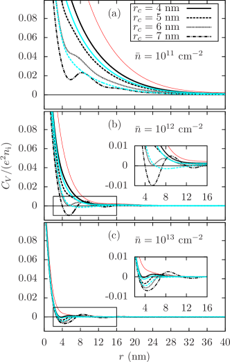
In Fig. 1 we consider a two-layer structure that consists of semi-infinite regions of SiO2 and air with graphene placed on the surface of SiO2, and a planar layer of point-charge impurities embedded in SiO2 a distance nm away from graphene. We show the radial dependence of the ACF for several values of and for different correlation lengths that are treated by both the SC and the HD models. One notices in Fig. 1 that the overall range of the ACF decreases with increasing owing to the screening by graphene, which is characterized by the screening length where is the Fermi wavenumber of graphene. More importantly, one notices in Fig. 1 that oscillations develop in the ACF for increasing and values, with no oscillations ever observed for the uncorrelated impurities with . For sufficiently large and values both the SC and the HD models give rise to negative values in the ACF over certain intervals of the radial distance . While the SC model gives more articulate oscillations than the HD model for the same value of , its domain of applicability is limited to correlation lengths nm for the given value of cm-2 because the SC model breaks down for . On the other hand, the HD model allows the use of much larger values than the SC model, giving rise to stronger oscillations in the ACF than those that could be achieved with the SC model. Remarkably, for the highest value of shown in Fig. 1(c), one notices that the second zero in the ACF in the HD model occurs at a distance that is approximately equal to the corresponding correlation length . This may be rationalized by noticing that, due to heavy screening by graphene at large , the fluctuations in both the electrostatic potential and the charge carrier density in graphene resemble the geometric structure of the underlying charged impurities represented by hard discs with the diameter . In view of this finding it is interesting to note that the values of the second zero in the ACF found in various experiments are quite large: 30 nm Zhang_2009 , 65-90 nm Deshpande_2011 , and 18 nm. Gomez_2012
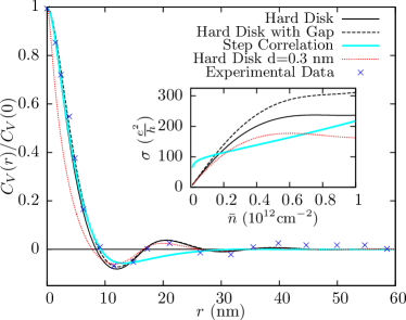

In Fig. 2 we attempt to model the normalized ACF of the potential, , deduced from the experimental data for graphene on SiO2, Gomez_2012 by using and the distance of impurities from graphene as fitting parameters, while assigning to and the values commensurate with those found in the experiment. We find the best fit to the experiment by using the HD model with nm for cm-2 (giving ) and cm-2, while setting nm, which is commensurate with distances used in modeling of the conductivity of graphene on SiO2. PNAS_2007 ; Sarma_2011 We also show in Fig, 2 two other results for the HD model with the same , and values, where we reduce the distance to 0.3 nm, or allow for a gap of air of thickness 0.3 nm between graphene and the SiO2 surface while keeping 1 nm. Ishigami_2007 ; Romero_2008 Also shown is the best fit with the SC model that is achieved for nm (giving ) with all other parameters having the same values as those used for the best fit with the HD model.
In the inset to Fig. 2 we show the conductivity as a function of for graphene on SiO2 evaluated from the semiclassical Boltzmann transport theory for the four cases discussed in the main panel.PNAS_2007 ; Sarma_2011 ; Anicic_2013 One notices a linear increase of at small (with a much larger slope for the SC model than for the HD model), followed by a sublinear behavior of at large values, which is represented by a reduction in the slope of for the SC model and a saturation in for the HD model.Anicic_2013
One notices in Fig. 2 that the existence of a finite gap of air has negligible effect on the ACF in the HD model, but noticeably reduces the saturation rate in the conductivity at high values. On the other hand, a reduction of the distance of impurities with zero air gap reduces the width of the main peak in the normalized ACF, which extends for distances from to the first zero in ACF, and accentuates the saturation in the conductivity in the HD model at high values. Most importantly, besides reproducing the main peak and the first zero of the normalized ACF, the SC model fails to reproduce the shape of the experimental ACF including its second zero and the subsequent peaks and valleys, which are well reproduced by the HD model. We note that our using the packing fraction of stretches the SC model to its breakdown point, whereas reduction in the packing fraction would further worsen the agreement of the SC model with the experiment. Therefore, one may conclude that the structure of the normalized ACF in this example is a result of a rather strong correlation among the charged impurities with the correlation length of nm that gives rise to a large packing fraction , which may be reliably described by the HD model.
It should come as no surprise that the correlation lengths among charged impurities may reach such large values in the presence of graphene. It was recently shown that the interaction potential between two point charges near doped graphene is heavily screened and, moreover, exhibits Friedel oscillations with inter-particle distance, giving rise to a repulsive core region of distances on the order of that resembles the interaction among hard disks with diameter .Radovic_2012
In Fig. 3 we consider single layer graphene sandwiched between a semi-infinite layer of SiO2 and a layer of HfO2 of finite thickness , which is typical for top-gating through a high- dielectric.Ong_2012 ; Fallahazad_2010 ; Hollander_2011 We show the radial dependence of the ACF for several combinations of the and values, and for several model distributions of point-charge impurities in the HfO2 layer having the areal number density cm-2. We consider a homogeneous 3D distribution of uncorrelated charges throughout the HfO2, which extends up to a distance 0.3 nm from graphene, as well as a 2D planar distribution placed in HfO2 a distance 0.3 nm away from graphene, with both uncorrelated () and correlated ( nm, ) charges that are described with the HD model. In comparison to Fig. 1, one notices that ACF has generally smaller magnitude in Fig. 3 because of stronger screening due to much larger dielectric constants involved. Moreover, comparing various cases of the distribution of impurities in Fig. 3, one notices that the ACF has a much lower magnitude in the case of a 3D distribution than in the corresponding 2D cases because the impurities are spread over larger distances from graphene in the 3D case and hence the resulting potential and its fluctuations are weaker. One further notices in Fig. 3 that a reduction in thickness suppresses the overall range of the ACF in a similar manner as does the increase in , which is caused by the increased screening due to the proximity of a perfectly conducting gate on the opposite boundary of the HfO2 layer from graphene. This increased screening by the gate is also responsible for the more articulated oscillations in the ACF for smaller thicknesses .
In conclusion, we have shown that both an increase of charge carrier density in graphene and a reduction of the distance of a nearby gate provide strong screening effects in the autocorrelation function (ACF) of the electrostatic potential in graphene. Those effects help reveal spatial correlation between charged impurities in the dielectric through appearance of oscillations of the ACF as a function of distance that exhibit well-defined intervals of anti-correlation in the potential. We have found that the second zero in the ACF is related to the correlation length for a 2D distribution of impurities, which may take quite large values, according to several experiments. Consequently, statistical models for the structure of charged impurities near graphene must be able to tackle systems with large packing fractions, resembling charged 2D fluids.
Acknowledgements.
This work was supported by the Natural Sciences and Engineering Research Council of Canada.References
- (1) Ph. Avouris and F. Xia, MRS Bulletin 37, 1225 (2012).
- (2) M. J. Allen, V. C. Tung, and R. B. Kaner, Chem. Rev. 110,132 (2010).
- (3) M. Ishigami, J. H. Chen, W. G. Cullen, M. S. Fuhrer, and E. D. Williams, Nano Lett. 7, 1643 (2007).
- (4) H. Romero, N. Shen, P. Joshi, H. R. Gutierrez, S. A. Tadigadapa, J. O. Sofo, and P. C. Eklund, ACS Nano 2, 2037 (2008).
- (5) J. Martin, N. Akerman, G. Ulbricht, T. Lohmann, J.H. Smet, K. Von Klitzing, and A. Jacoby, Nat. Phys. 4, 144 (2008).
- (6) Y. Zhang, V.W. Brar, C. Girit, A. Zettl, M.F. Crommie, Nat. Phys. 5, 722 (2009).
- (7) A. Deshpande, W. Bao, Z. Zhao, C. N. Lau, and B. J. LeRoy, Appl. Phys. Lett. 95, 243502 (2009).
- (8) A. Deshpande, W. Bao, Z. Zhao, C. N. Lau, and B. J. LeRoy, Phys. Rev. B 83, 155409 (2011).
- (9) A. Castellanos-Gomez, R. H. M. Smit, N. Agrait, and G. Rubio-Bollinger, Carbon 50, 932 (2012).
- (10) Y.-W. Tan, Y. Zhang, K. Bolotin, Y. Zhao, S. Adam, E. H. Hwang, S. Das Sarma, H. L. Stormer, and P. Kim, Phys. Rev. Lett. 99, 246803 (2007).
- (11) S. Adam, E. H. Hwang, V. M. Galitskii, and S. Das Sarma, Proc. Natl. Acad. USA 104, 18392 (2007).
- (12) S. Das Sarma, S. Adam, E. H. Hwang, and E. Rossi, Rev. Mod. Phys. 83, 407 (2011).
- (13) J. Yan and M. S. Fuhrer, Phys. Rev. Lett. 107, 206601 (2011).
- (14) Q. Li, E. H. Hwang, E. Rossi, and S. Das Sarma, Phys. Rev. Lett. 107, 156601 (2011).
- (15) H. Yan, T. Low, W. Zhu, Y. Wu, M. Freitag, X. Li, F. Guinea, P. Avouris, and F. Xia, Nat. Photonics 7, 394 (2013).
- (16) Z.-Y. Ong and M. V. Fischetti, Phys. Rev. B 86, 121409(R) (2012).
- (17) Z.L. Miskovic, P. Sharma and F. O. Goodman, Phys. Rev. B 86, 115437 (2012).
- (18) R. Anicic and Z. L. Miskovic, arXiv:1307.8169 (2013).
- (19) B. Fallahazad, S. Kim, L. Colombo, and E. Tutuc, Appl. Phys. Lett. 97, 123105 (2010).
- (20) M. J. Hollander, M. LaBella, Z. R. Hughes, M. Zhu, K. A. Trumbull, R. Cavalero, D. W. Snyder, X. Wang, E. Hwang, S. Datta, and J. A. Robinson, Nano Lett. 11, 3601 (2011).
- (21) Y. Rosenfeld, Phys. Rev. A 42, 5978 (1990).
- (22) B. Wunsch, T. Stauber, F. Sols, and F. Guinea, New J. Phys. 8, 318 (2006).
- (23) E. H. Hwang and S. Das Sarma, Phys. Rev. B 75, 205418 (2007).
- (24) I. Radovic, D. Borka, and Z. L. Miskovic, Phys. Rev. B 86, 125442 (2012).