Parameters Influencing the Optical Properties Of SnS Thin Films
Abstract
Tin Sulphide (SnS) thin films have been recognized as a potential candidate for solar cells. Many fabrication techniques have been used to grow SnS thin films. The band-gap, of SnS films as reported in literature, were found to vary from 1.2-2.5 eV depending on the film fabrication technique. The present work reports the structural, compositional, morphological and optical characterization of SnS thin films fabricated by thermal evaporation at room temperature. Results show that for the given fabrication technique/ condition, the band-gap functionally depends on the lattice parameter and grain size. The well-defined variation allows for tailoring SnS film as per requirement.
1 Introduction
Tin Sulphide (SnS) is formed from elements belonging to the IV-VI group of the periodic table [1]. Like other sulphide compounds ( and etc.), SnS too attracted attention in the 1970 and 1980’s for possible application as an optical storage medium [2, 3]. However, recent investigations are directed towards studying its potential as a photovolatic or solar cell essentially due to its high absorption coefficient, low cost and low toxicity [4, 5]. A pertinent point is that both applications require SnS to be in its thin film state. Being a layered chalcogenide [6, 7] of relatively low melting point [8], SnS has been found to be a suitable candidate for thin film fabrication. Depending on film thickness, the color of SnS films varies from orange to brown when viewed in transmission. Thus, the last 30-40 years has seen substantial work in fabrication of SnS thin films using various methods like thermal evaporation [9], RF sputtering [10], chemical vapor deposition [11], electrodeposition [12] and spray pyrolysis [13]. The reported optical band-gap of SnS films lies between 1.1-2.1 eV [14, 15] depending on the fabrication method used.
While there are large number of reports on SnS, more systematic studies should be undertaken considering its potential commercial application as a solar cell. Especially to understand why the band-gap of SnS varies so much. With this intention, we have carried out systematic studies on SnS thin films of varying thicknesses grown by thermal evaporation. The structural, morphological, compositional and optical properties of the films are reported here. The role of the intra-planar forces in the layer structured (as seen from the lattice parameters of unit cells within the nano-crystalline SnS grains) and the grain size on the band-gap of the films have been discussed.
2 Experimental
SnS thin films of varying thickness were grown on glass substrates maintained at room temperature by thermal evaporation at vacuum better than Torr. A Hind High Vac (12A4D), Bengaluru thermal evaporation coating unit was used for the thermal evaporation process. SnS powder of 99% purity supplied by Himedia (Mumbai) was used as the starting material. The thicknesses of the as grown films were then measured by a Veeco Dektak Surface Profiler (150). The standard structural, morphological and optical characterization of the films were done using Bruker D8 Diffractometer (in the mode), Renishaw Invia Raman Microscope, Field-Emission Scanning Electron Microscopy (FE-SEM FEI-Quanta 200F) and Systronics UV-VIS Double beam Spectrophotometer (2202). Chemical composition of the films were determined using Kratos Axis Ultra DLD’s X-Ray Photoelectron Spectroscopy (XPS) with target.
3 Results and Discussion
3.1 Structural Studies
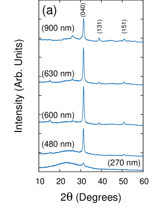
The X-Ray diffractograms of very thin SnS films (thickness less than 150 nm) were unmarked with a hump between () . The absence of peaks suggests that the samples were not crystalline. This is not surprising since chalcogenides grown at room temperature are usually amorphous in nature. However, the hump indicates that there might be some short range order among the atoms. As the sample thickness increases (270 nm and above), a small diffraction peak emerges on the hump around . Thus, it would appear that ordering increases with increasing film thickness. Fig (1a) shows the X-Ray diffraction patterns of samples of different thicknesses. The peak positions matched with those reported in ASTM Card No. 83-1758 implying an orthorhombic unit cell structure with lattice parameters of 4.148, 11.48 and 4.177 Å. The standard relationship [18] was used to determine the lattice parameters using the peak positions
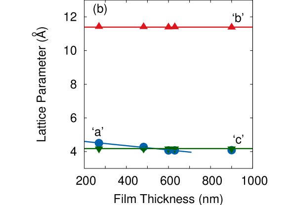
The lattice parameters ‘b’ and ‘c’ were found to be and respectively. The lattice parameters were found to remain constant with increasing film thickness within experimental error (fig 1b). Fig (1b) however, shows an initial decreasing trend of lattice parameter ‘a’ with increasing film thickness. However, for film thicknesses greater than 600 nm, there is no tensile stress acting on the films and ‘a’ remains constant.
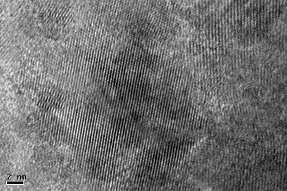
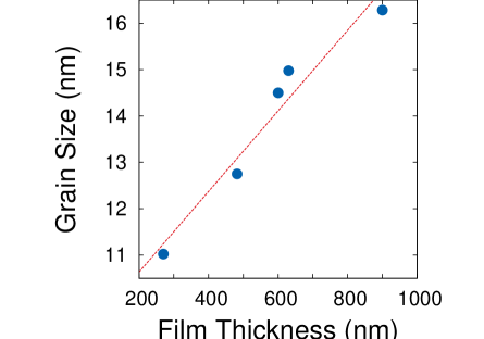
Fig 2 is a Transmission Electron Microscope (TEM) image of a 480 nm thick film. The image clearly shows the layered nature of the SnS films. The interplanar distances was found to be 2.45Å (). This would mean the films are oriented with the (040) plane lying parallel to the substrate. The oriented nature of the films is also seen in the XRD patterns with the (040) peak standing out as the most intense peak in agreement with observations reported [16, 17]. The X-Ray diffraction peak’s Full Width at Half Maxima (FWHM) gives the grain size using Scherrer formula [18]. Fig (3) shows a linear relationship between the average grain size and film thickness.
3.2 Raman Spectra and XPS Analysis
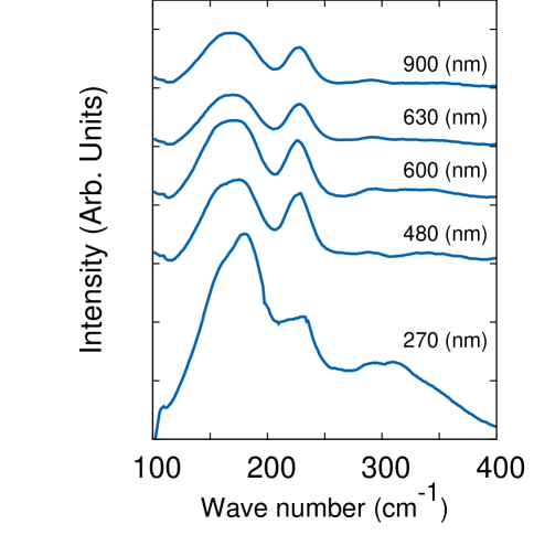
The Raman spectra of SnS thin films were collected using Argon laser in back scattering mode. The laser power (15 mW), exposure time (30 sec) and beam area were maintained constant for all the samples. Since SnS is known to show changes induced by photo-thermal absorption of light [2, 3], all the Raman spectra were collected using low power laser. The nano-crystalline samples showed three prominent peaks which were consistently present in all the samples (fig 4) in varying proportions around , and . However, each sample showed slight displacement in peak position compared to those reported for single crystal Raman peaks [6]. The consensus in literature is that the peak indicates existence of [19]. This may have resulted due to the growth technique, since starting material’s Raman does not exhibit peak at . The contribution decreases with thickness as is evident from the decreasing peak intensity and area with increasing film thickness.
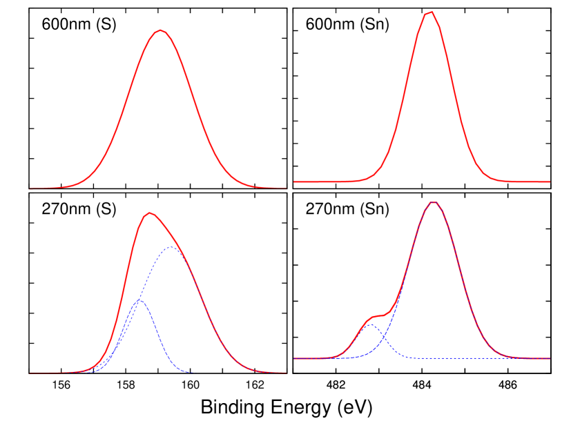
This was also confirmed by the chemical composition analysis done on the films of different thicknesses using X-Ray Photo-electron Spectroscopy (XPS). Fig 5 compares the XPS peaks of sulphur and tin for 270 and 600 nm thicknesses. The 600 nm thick sample had lone sulphur 2p and tin peaks that could not be deconvoluted. The number of sulphur () and tin atoms () in bonding per area can be evaluated using the area under the curve () and cross-sectional values () [20] in the standard formula [21]
The ratio of sulphur to tin in this sample was found to be , suggesting within experimental error that the 600 nm sample is of SnS. However, in comparison with this, the 270 nm sample’s sulphur (2p) and tin () peaks can be deconvoluted into two peaks. Based on the Raman results, we associate the major peaks with SnS and the minor ones with . Using the above mentioned formula and area under the curves, the ratio of S/Sn from the major peaks give 1.1 while from the minor peaks . Thus, thin samples (270 nm and 480 nm) have both species of SnS and . From the ratio of two tin peaks, we may say only of the film is .
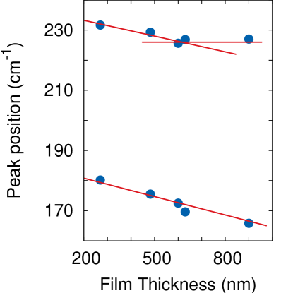
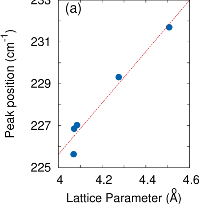
The peak or the peak is associated with interaction along the inter-layer ‘b’ axis [22] while the peak is the symmetric Sn-S bond’s stretching mode () [15]. As the film thickness increases, the position of these two peaks shifts (Fig 6 shows the variation). Initially, the peak position of was found to decrease with increasing film thickness, however, after 600 nm the peak position remained fixed . The region of saturation corresponds to where samples have constant lattice parameters. Hence, we believe that the peak position of is intimately related to the lattice size. A plot between and ‘a’ (fig 6a) confirms a linear relation between the two. An increase in wave-number (vibration frequency) marks the increase in restoring force (bond strength). Hence, the results suggest that increasing tensile stress along ‘a’ direction is accompanied with increased restoring force acting between the tin and sulphur atom.
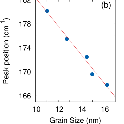
Fig 6 exhibits the variation in peak position with film thickness. This shows a monotonous decrease with film thickness. Shift in Raman peak position may also be related to grain size [23]-[27] and nature of defect on the grain boundaries [28]. Fig (7b) plots peak position with respect to the grain size. We find that the plot conforms to results of Zhu et al [29] where a shift to lower wave numbers takes place with increasing grain size. As reported, SnS are layered compounds with layers formed by ‘Sn’ and ‘S’ zig-zagged molecules. These layers arrange themselves normal to the ‘b’ axis with weak Van der-Waal “inter-planar” forces acting between them. The layers themselves, due to this zig-zagging, have finite thickness with strong “intra-planar” forces acting within it. If any stress acts along the ‘b’ axis, the “inter-planar” distances vary with no effect on the “intra-planar” distances [30]. Variation in grain size seems to effect “inter-planar” distances, thus effecting peak position. Increased grain size is accompanied with lower Raman wave-numbers and hence indicate lower restoring forces, which from our above analysis on , would imply lattice constant ‘b’ would decrease with increasing grain size. However, the variation in ‘b’ () as seen from X-Ray Diffraction results) is too small to justify this comment.
3.3 Morphological Studies
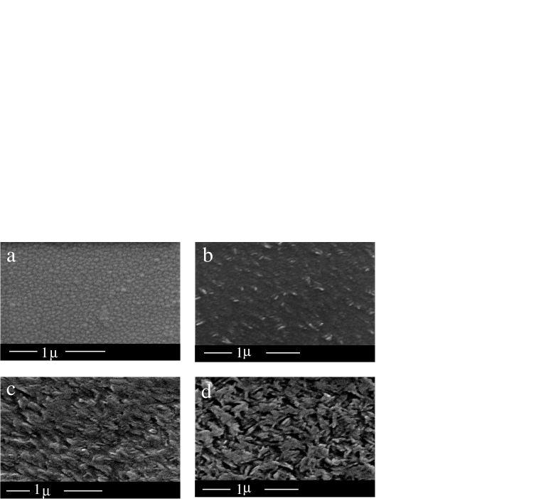
Fig (8) shows representative SEM images of SnS as grown films of different thicknesses, namely 150, 480, 600 and 900 nm. The grain morphologies are similar to those reported earlier [31]. In the case of the thicker films (480, 600 and 900 nm), the morphology of the films appear very similar to each other, with noticeable increase in grain density with increasing film thickness. However, the morphology of the 150 nm thick film is distinctly different consisting spherical grains. As discussed above, Raman spectra (fig 4) and XPS analysis clearly shows that this sample contains . This should explain the distinctly different morphology of this sample from the remaining samples. Though results related to this sample have not been used in this present study, we have included its SEM to show very thin films are dominated with marked by spherical grains. Grains of these morphology are absent in samples with thicknesses greater than 250 nm, highlighting, no or negligible contribution by in these samples.
3.4 Optical Studies
The absorption spectra of as grown SnS films with varying thicknesses were obtained between 300 and 1100 nm at room temperature. The band-gaps were evaluated using the absorption coefficient ‘’ obtained from the UV-visible spectra using standard formula [32]
where ‘A’ and ‘t’ are the film’s absorbance and thickness respectively. The band-gap of the films can be evaluated from this information. SnS is reported to have both indirect [15] and direct band-gap [33]. Band-gaps are usually evaluated using Tauc’s method [34] where a graph between is plot with respect to . The linear region of this plot is extrapolated to intersect the ‘X’-axis at y=0. The point of intersection gives the band-gap of the material. For direct allowed transitions, the absorption coefficient is related to the photon energy by equation [35]-[38]
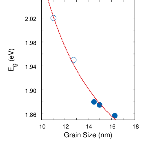
where ‘K’ is the proportionality constant. Fig (9) shows the variation of the band-gap with grain size. The 270 and 480 nm thin films have a considerably large band-gap. While one may suspect this to be due to the existence of in these samples, it should be noted that only of the sample is . They are predominantly SnS films. Also, the linear trends shown in fig 7(a) and (b) argue little or no significant contributions are made by . We hence shall assume the large energy band-gaps to be manifestations of structural and morphological trends of SnS. Before commenting on this however, notice the nature of band-gap variation with grain size. Experimental data fits to
| (1) |
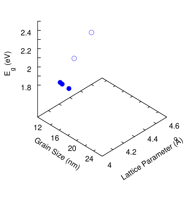
where ‘r’ is the radius of the nanoparticle and ‘M’ the effective mass of the system. In other words, the band-gap is inversely proportional to the grain size. This fit suggests quantum confinement of the electrons [39]. Note that the data points represented by unshaded circles in fig (9) have different ‘a’ lattice parameter. Fig (10) uses the same data points of fig (9), abid in three dimension. We can now see the band-gap dependence on both grain size and lattice parameter. Mathematically, the band-gap of SnS nano-crystalline thin films is a two variable function of grain size and lattice parameter, . While the relation between the band-gap and grain size is a well known (eqn 1), there is no known relation between the band-gap and lattice parameter (‘a’). Hence, more studies would be required to establish the observed two variable dependency.
Conclusion
Tin sulphide films grown on glass substrates at room temperature by thermal evaporation were found to be nano-crystalline in nature for thicknesses more than 270 nm. X-Ray diffraction shows that the grain size increased linearly with film thickness. Diffraction studies and Electron microscope images show that the atoms of SnS are arranged in an layered and oriented manner with ortho-rhombic structure and residual tensile stress acting along the ‘a’ axis. The films had direct band-gaps ranging from 1.8-2.1 eV depending on the grain size and lattice parameter. Thus, the study reveals that the band-gap of SnS is a two variable function, which can be tailored as per requirement by controlling the grain size and lattice parameter.
Acknowledgment
Authors are grateful to the Department of Science and Technology for funding this work under research project SR/NM/NS-28/2010.
References
- [1] Chakrabarti A., Lu J., McNamara A.M., Kuta L.M., Stanley S.M., Xiao Z., Maguire J.A., Hosmane N.S. Tin(IV) sulfide:Novel nanocrystalline morphologies. Inorg Chim Acta, 2011, 374:627
- [2] Yue G.H., Wang L.S., Wang X., Chen Y.Z., Peng D.L. Characterization and Optical Properties of the Single Crystalline SnS Nanowire Arrays Nanoscale Res Lett, 2009, 4:359
- [3] Patil S.G., Tredgold R.H. Electrical and photoconductive properties of crystals. J Pure Appl Phys, 1971, 4:718
- [4] Wang Z., Qu S., Zeng X., Liu J., Zhang C., Tan F., Jin L., Wang Z. The application of SnS nanoparticles to bulk heterojunction solar cells. J Alloys Comp, 2009, 482: 203
- [5] Noguchi H., Setiyadi A., Tanamora H., Nagatomo T., Omoto O. Characterization of vacuum-evaporated tin sulfide film for solar cell materials. Sol. Energy Mater. Sol. Cells, 1994, 35:325
- [6] Nikolic P.M., Miljkovic Lj., Mihajlovic P., Lavrencic B. Splitting and coupling of lattice modes in the layer compound SnS. J Phys C: Solid State Phys, 1977, 10: L289
- [7] Makinistian L., Albanesi E.A. Study of the hydrostatic pressure on the orthorhombic IV-VI compounds including many-body effects. J Comput Mater Sci, 2011, 50:2872
- [8] “CRC Handbook of Chemistry and Physics (1993-1994)” Edn., Ed. Linde D.R. (Boca RA Raton, FL: CRC Press).
- [9] El-Nahass M.M., Zeyada N.M., Aziz M.S., El-Ghamaz N.A. Optical properties of thermally evaporated SnS thin films. Opt Mater, 2002, 20:159
- [10] Hartman K., Johnson J.L., Bertoni M.I., Recht D., Aziz M.J., Scarpulla M.A., Buonassis T. SnS thin-films by RF sputtering at room temperature. Thin Solid Films, 2011, 519:7421
- [11] Nair M.T.S., Nair P.K. Simplified chemical deposition technique for good quality SnS thin films. Semicond Sci Technol, 1991, 6:132
- [12] Ghazali A., Zainal Z., Hussein M.Z., Kassim A. Cathodic electrodeposition of SnS in the presence of EDTA in aqueous media. Sol. Energy Mater. Sol. Cells, 1998, 55:237
- [13] Thangaraju B., Kaliannan P. Spray Pyrolytic deposition and characterization of SnS and . J Phys D: Appl Phys, 2000, 33:1054
- [14] Gao C., Shen H., Sun L. Preparation and properties of zinc blende and orthorhombic SnS films by chemical bath deposition. Appl Surf Sci, 2011, 257:6750
- [15] Sohila S., Rajalakshmi M., Ghosh C., Arora A.K., Muthamizhchelvan C. Optical and Raman scaterring studies on SnS nanoparticles. J Alloy Compd, 2011, 509:5843
- [16] Yue G.H., Wang W., Wang L.S., Wang X., Yan P.X., Chen Y., Peng D.L. The effect of annealing temperature on physical properties of SnS films. J Alloy Compd, 2009, 474:445
- [17] Jiang F., Shen H., Gao C., Liu B., Lin L., Shen Z. Preparattion and properties of SnS film grown by two-stage process. Appl Surf Sci, 2011, 257:4901
- [18] Cullity B.D., Stock S.R., “Elements of X-Ray Diffraction”, Ed., Prentice-Hall Inc (NJ, 2001)
- [19] Lucovsky G., Mikkelsen J.C., Liang W.Y., White R.M. Optical phonon anisotropies in the layer crystals and . Phys Rev B, 1976, 14:1664
- [20] Band I.M., Kharitonov Y.I., Trzhaskovskaya M.B. Photoionization cross sections and photoelectron angular distributions for x-ray line energies in the range 0.132–4.509 keV targets: 1 ≤ Z ≤ 100. At Data Nucl. Data Tables, 1979, 23:443
- [21] Briggs D. “Handbook of X-ray and Ultra-voilet Photo-electron Spectroscopy”, Perkin-Elmer Corportation. Physical Electronics Division, 1978
- [22] Chandrasekhar H.R., Humphreys R.G., Zwick U.,Cardona M. Infrared and Raman spectra of the IV-VI compounds SnS and SnSe. Phys Rev B, 1977, 15:2177
- [23] Choi H.C., Jung Y.M., Kim S.B. Size effects in Raman spectra of nanoparticles. J Vib Spectrosc, 2005, 37:33
- [24] Rajalakshmi M., Arora A.K., Bendre B.S., Mahamuni S. Optical phonon confinement in zinc oxide nanoparticles. J Appl Phys, 2000, 87:2445
- [25] Yang C.L., Wang J.N., Ge W.K., Guo L., Yang S.H., Shen D.Z. Enhanced Ultraviolet emission and optical properties in polyvinyl pyrrolidone surface modified ZnO quantum dots. J Appl Phys, 2001, 90:4489
- [26] Guo L., Yang S., Yang C., Yu P., Wang J., Ge W., Wong G.K.L. Highly monodisperse polymer-capped ZnO:nanoparticles: Preparation and optical properties. Appl Phys Lett, 2000, 76:2901
- [27] Alim K.A., Fonoberov V.A., Balandin A.A. Origin of the optical phonon frequency shifts in ZnO quantum dots. Appl Phys Lett, 2005, 86:053103-1
- [28] Kitahara K., Ishii T., Suzuki J., Bessyo T., Watanabe N. Characterization of Defects and Stress in Polycrystalline Silicon Thin Films on Glass Substrates by Raman Microscopy. INT J Spectrosc, 2011, 2011:1
- [29] Zhu J.S., Lu X.M., Jiang W., Tian W., Zhu M., Zhang M.S., Chen X.B., Liu X., Wang Y.N. Optical study on the size effects in BaTiO3 thin films. J Appl Phys, 1997, 81:1392
- [30] Ehm L., Knorr K., Dera P., Krimmel A., Bouvier P., Mezouar M. Pressure induced structural phase transition in the IV-VI semiconductor SnS. J Phys:Condens Mater, 2004, 16:3545
- [31] Devika M., Reddy N.K., Ramesh K., Ganesan V., Gopal E.S.R. ,Reddy K.T.R. Influence of substrate temperature on surface structure and electrical resistivity of the evaporated tin sulphide films. Appl Surf Sci, 2006, 253:1673
- [32] Streetman B. “Solid State Electronic Devices”, Ed., PHI (New Delhi, 1995).
- [33] Devika M., Reddy N.K., Prashantha M., Ramesh K., Reddy S., Hahn Y.B., Gunasekhar K.R. The physical properties of SnS films grown on lattice-matched and amorphous substrates. Phys Status Solidi A, 2010, 207:1864
- [34] Tauc J. Absorption edge and internal electric fields in amorphous semiconductors. Mat. Res. Bull., 1970, 5:721
- [35] Mott N.F., Davis E.A. “Electronic Process in Non-Crystalline Materials”, Clarendon Press (Oxford, 1979).
- [36] Pankove J.I. “Optical Processes in Semiconductors”, PHI, NY (1971).
- [37] Tauc J. “Amorphous and Liquid Semiconductors”, J. Tauc Ed., Plenum, London (1974).
- [38] Clark A.H. “Polycrystalline and Amorphous Thin Films and Devices”, Kazmerski L. Ed., Academic Press (NY, 1980).
- [39] Brus L.E. Electron–electron and electron‐hole interactions in small semiconductor crystallites: The size dependence of the lowest excited electronic state. J Chem Phys, 1984, 80:4403
Figure Captions
-
1.
Fig (a) compares the X-Ray Diffraction Pattern of SnS films of various thicknesses. The sample thicknesses and Miller indices are also indicated. Alongside, (b) shows the variation in lattice parameters with film thickness.
-
2.
TEM micrograph of a 480 nm thin film shows the layered structure of SnS thin film.
-
3.
The average grain sizes of SnS films were found to be linearly proportional to the film thickness.
-
4.
Raman spectra of SnS thin films of various thicknesses show existence of three prominent peaks at , and (Refer to text).
-
5.
XPS peaks of tin and sulphur for 270 and 600 nm thick films are visibly different. The 270 nm sample’s XPS peaks can be deconvoluted into two peaks, indicating presence of SnS (major contribution) and (minor contributrion). The peaks from are absent in the 600 nm sample, thus showing thicker films are of SnS.
-
6.
Variation of Raman peak positions with film thickness. Both and show a decreasing trend with film thickness. However, levels out for film thicknesses above 600 nm (the curve looks similar to that of fig 1b).
-
7.
The (a) peak position is found to depend on the lattice parameter ‘a’ while (b) peak position shows dependence on grain size.
-
8.
Scanning electron micrographs (SEM images) of SnS thin films of thicknesses (a) 150, (b) 480, (c) 600 and (d) 900 nm.
-
9.
Graph shows the variation in band-gap with grain size for as grown SnS thin films. The filled circles represent samples that have the same lattice parameters while unfilled circles represent samples with varying grain size and lattice parameter. The solid curve is the best fit of eqn (1) to the data points. The fit suggests band-gap variation is a result of the electron’s quantum confinement within the grain.
-
10.
Three dimension plot shows band gap dependence on lattice parameter ‘a’ and grain size. The filled and unfilled circles representing data points are as explained for fig 9.