Out of equilibrium charge dynamics in a hybrid cQED architecture
Abstract
The recent development of hybrid cQED allows one to study how cavity photons interact with a system driven out of equilibrium by fermionic reservoirs. We study here one of the simplest combination : a double quantum dot coupled to a single mode of the electromagnetic field. We are able to couple resonantly the charge levels of a carbon nanotube based double dot to cavity photons. We perform a microwave read out of the charge states of this system which allows us to unveil features of the out of equilibrium charge dynamics, otherwise invisible in the DC current. We extract relaxation rate, dephasing rate and photon number of the hybrid system using a theory based on a master equation technique. These findings open the path for manipulating other degrees of freedom e.g. the spin and/or the valley in nanotube based double dots using microwave light.
pacs:
73.23.-b,73.63.FgConfined electronic states in quantum dot circuits allow one to encode and manipulate quantum information. Double quantum dot structures are particularly appealing in that context because they can be described with a simple Hilbert space, yet providing the necessary control for quantum manipulation of spin or charge degrees of freedomHanson:05 .
Recently, on-chip photonic cavities coupled to the charge of double quantum dots have appeared as a promising new toggle for manipulating quantum informationFrey:12 ; Petta:12 ; Toida:13 ; Basset:13 . Such a hybrid circuit quantum electrodynamics (cQED) architecture can be used to read out single quantum dots Delbecq:11 and to couple distant quantum dot circuits Delbecq:13 . It could also be used to couple coherently distant spins and read them out in a quantum non-demolition manner Raimond:01 provided the strong spin/photon coupling is achieved. The latter requires a large spin photon coupling strength and long spin dephasing times. Both theses features remain to be observed in the double dots cQED structures demonstrated so far.
Single wall carbon nanotubes are interesting in that context because they provide, in contrast to the other platforms based on InAs nanowires or GaAs/AlGaAs two dimensional electron gas, a nuclear spin free environment if grown with isotopically pure . Furthermore, they can easily be coupled to various kinds of electrodes which could lead to new spin manipulation schemesTrif:08 ; Cottet:10 ; Nori:12 ; Cottet:12 ; Skoldberg:06 ; Jin:11 .
In this letter, we demonstrate that we can embed nanotube based double quantum dots into high quality factor microwave cavities. We demonstrate that these devices behave like an effective spin which can be brought into resonance with the cavity photons. We use the cavity to read-out this effective spin in out of equilibrium conditions e.g. when a large power is applied to the cavity or a finite bias is applied to the double quantum dot (DQD). Finally, we are able to observe the microwave spectroscopy of the charge levels using a two-tone drive scheme. This method could be easily generalized to characterize other types of degrees of freedom e.g. the spin and/or the valley Laird:13 .
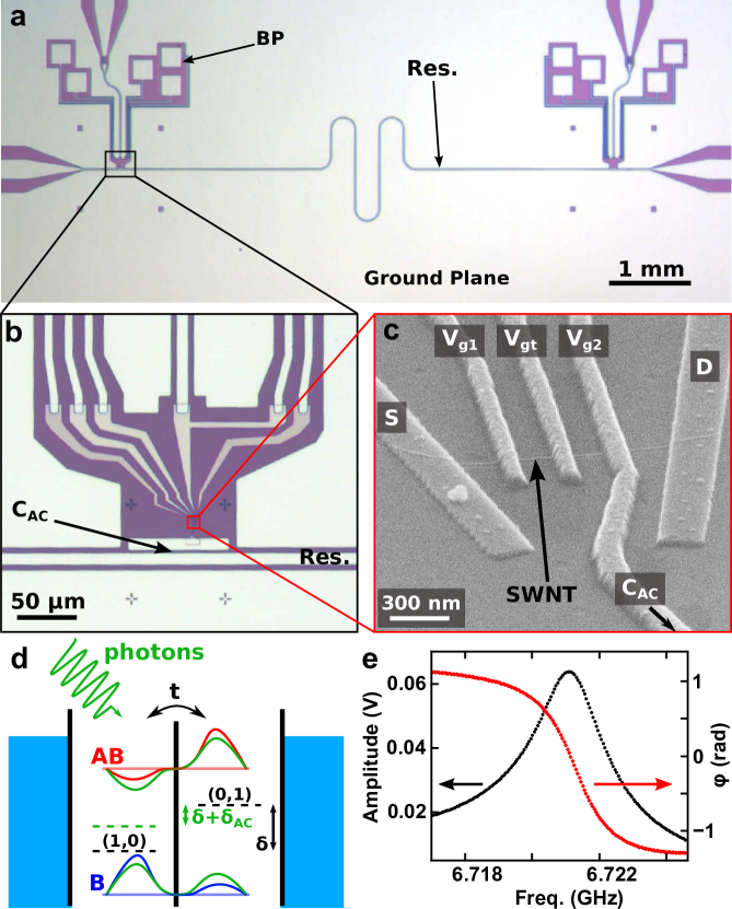
The devices are fabricated using a novel stamping techniquestampingViennot:13 which allows us to combine highly isolated nanotube based double quantum dot devices and high quality factor microwave cavities, adapted from Pei:12 ; ChineseNanolett:11 ; ChineseNanolett:11b . The nanotube device is fabricated using standard lithography techniques in two steps. The top gates are fabricated using 3 oxidations/evaporation of thick Al layers under a pressure of for 10 min. The top gates are subsequently covered by of Al and of Pd. The second lithography step allows us to fabricate the source and the drain electrodes which are thick PdNi electrodes (see figure 1d). The third step is the fabrication of the microwave cavity using photolithography which allows us to make thick Al superconducting microwave resonators. The novel stamping technique is essential here for obtaining reliably quality factors larger than . We think that it is also essential for getting double quantum dot devices with an internal hopping strength comparable with the cavity frequency, which is very difficult in nanotube based quantum dots. The device presented in the present paper had a quality factor of about (even for a photon number smaller than ). The transmission amplitude and phase close to the resonance frequency is shown in figure 1f. Note the hammer finger starting from one of the topgates of the nanotube which is made to increase the asymmetry between the electron-photon couplings to the right and left dot. The resulting device is shown in figure 1b,c and d. In each of our cavity, we embed two double-dot circuits which could be used to explore non-local transport properties mediated by photons in such devices Delbecq:13 ; Bergenfeld:13 ; Bergenfeld:13b ; Contrerapulido:13 ; Nori:13 . The microwave setup used to measure the microwave response of the cavity is essentially similar to the one used in Delbecq:11 but with a cryogenic amplifier stage with a noise temperature of about . All the microwave measurements are performed at a frequency of and at a temperature of (electronic temperature about ).
The natural state basis for the DQD is the molecular state basis of the bonding and anti-bonding states respectively. We define . Such a system is a charge quantum bit which is naturally coupled to the microwave photons of the cavity. Provided the coupling between the photons and the two dots is asymmetric, one can map the hamiltonian of the system onto a Jaynes-Cummings hamiltonian of the pseudo-spin coupled to the cavity Frey:12 ; Jin:11 ; Petta:12 . We assume that we drive the cavity with a classical field of pulsation . Solving the coupled dynamics of the spin-photon system Viennot:14 yields the following dispersive shift for the cavity photons :
| (1) |
where is the susceptibility of the system. The parameters entering in are the charge-photon coupling strength , the hybridization angle , the qubit-microwave drive detuning , the energy difference between the bonding and anti-bonding states , the effective spin relaxation and dephasing rates and respectively.

As shown in figure 2, the phase is finite only at the degeneracy lines between (N,M) and (N-1,M+1) charges states, which is highlighted by a dashed line between the two triple points visible in the DC current in figure 2a. Such a phase contrast shows that photons couple mainly asymmetrically to the two dots and induce transitions from the left (L) to the right (R) dot and vice versa in this gate region Petersson:09 ; Cottet:11 . In figure 2d, the peak with lateral satellite dips of the phase show that the B/AB doublet becomes resonant with the cavity when the phase changes sign. The red line in figure 2f fits this phase contrast with equation (1) and , and allows to get . Depending on the setting of the 3 gates, we get values for and ranging from to and from to respectively. These figures are comparable to what is found in 2DEGs Frey:12 ; Toida:13 and in InAs nanowires Petta:12 . The non-linear photonic and/or electronic regimes which have not been investigated so far, allow one to get a deeper understanding of the double-dot/cavity hybrid system.
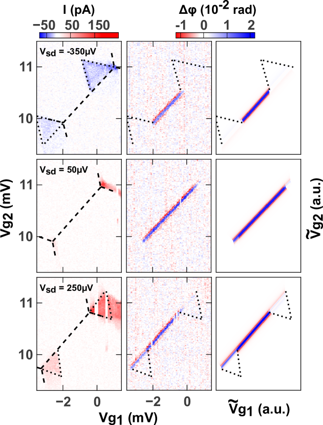
We now turn to the finite bias regime in the low power limit. Figure 3 displays the DC current and the cavity response for finite bias . This leads to characteristic transport triangles in the transport spectroscopy. These triangles indicate that the populations of the ground and first excited state are strongly out of equilibrium leading to which can a priori change sign under the triangles. As shown in figure 3, the phase contrast remains essentially identical at and in the linear regime of figure 2b, with a B/AB degeneracy line spanning between the two triple points of the double dot. At , the degeneracy line shrinks with weak phase contrast under the top red triangle and a finite residual contrast under the bottom red triangle. This means that is strongly reduced under the top triangle (equal population for the bonding and anti-bonding states) whereas it stays finite (negative) under the bottom triangle. This shows the interest of the microwave phase signal in this out of equilibrium situation. The top and bottom triangles are nearly identical and have similar current contrast, whereas the phase contrast is markedly different, because it directly reveals the value of . For opposite bias as illustrated in the top panel of figure 3 (), goes to zero under both triangles. This signals asymmetric coupling to the DQD leads. As shown in the rightmost panels of 3, we are able to reproduce the observed features with our theory Viennot:14 . Reproducing the features of the phase strongly constraints the bare lead couplings to for and for respectively. The latter large values probably signal that cotunneling contributes for this bias, although it is not visible in the current. In all cases, the internal relaxation rate is about .
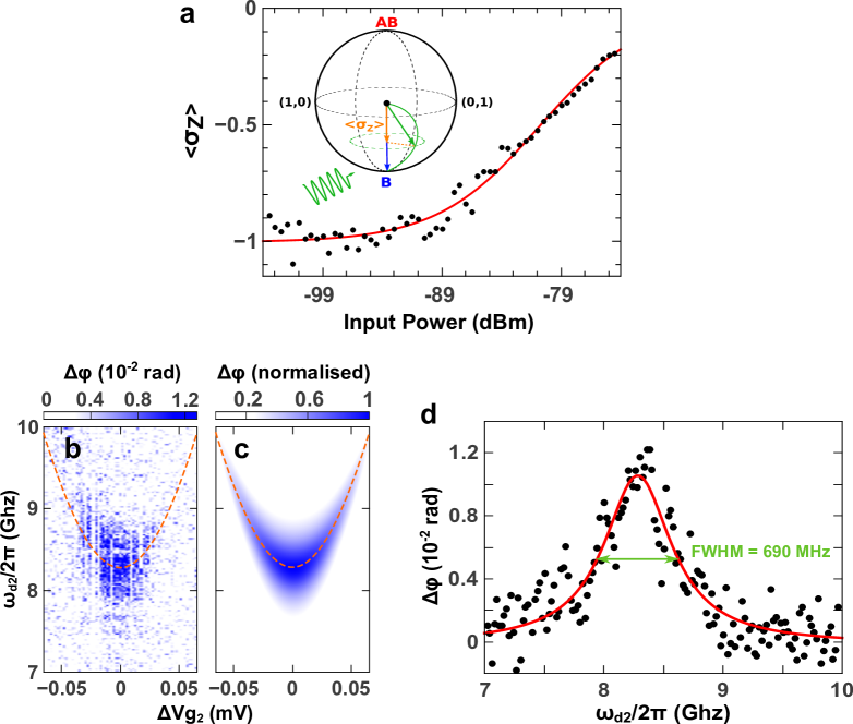
The power dependence of the phase contrast at zero detuning allows one to determine the ratio between the relaxation rate and the cavity photon number at a given power. As depicted in figure 4a in the inset, photons exert a transverse torque on average on the charge qubit effective spin towards the equatorial plane of the Bloch sphere, thereby reducing the value of . Since the photons drive the effective spin, the efficiency of this process is directly related to the relaxation rate of the effective spin. Our theory allows to fit quantitatively our data using the estimate of . Specifically, the fit with the red solid line of figure 4a corresponds to , being the number of photons in the cavity for an input power of . Using the estimate of , we find by fitting our data to the theory.
A microwave spectroscopy of the double dot can be performed by measuring the phase contrast at the cavity frequency while exciting the DQD with a second coherent field tone which one can bring in resonance with the bonding/antibonding doublet energy. This is conveniently done when the cavity and the DQD are not in resonance (). Defining the second microwave drive and , the overall dispersive shift reads :
| (2) |
The parameter is a coupling constant between the second tone drive amplitude which depends on whether the second tone is applied through the input port of the cavity or on a side port directly to a gate on the double quantum dot. We have used both methods and they give similar results. On figure 4b, we present such a measurement. We observe a spot in the detuning-second tone frequency plane around which is spreading around the zero detuning point. As highlighted by the dashed lines corresponding to the expected resonance frequency, this spot follows roughly the expected dispersion of the charge doublet. On figure 4c, we present the result of the modeling according to formula (2), in good agreement with the experimental map. As one can see from formula (2), such a measurement allows us to directly access to (which appears naturally in ) when the drive amplitude is sufficiently low (). We have checked that we were indeed in this regime for the measurements presented in figure 4. A cut of the measurement at zero detuning is presented in figure 4d. We observe a resonance centered around with a large amplitude of about . We can fit the data with the lorentzian line shape shown in red line in figure 4d, which is obtained from equation 2 (the large amplitude observed is however not fully understood). The full width at half maximum (FWHM) of about allows us to get , which is a bit lower than with the previous estimate of . The latter fact is consistent with the scaling law predicted by the simple dephasing model (see below), since is slightly higher here than in the previous sections (slightly different gate set).
The estimates made for allow us to determine for the gate setting presented in details in this paper and for another resonant region (not shown). Our lowest value reported is almost an order of magnitude lower than those reported in ref Frey:12 and Petta:12 . These figures are very important for future development of devices exploiting other degrees of freedom than the charge, like spin or valley, in carbon nanotubes. They allow us to give an upper bound of the typical charge noise in our device. Indeed, the magnitude of the dephasing rate is likely to be due to charge noise in the environment of the nanotube. Using a simple semiclassical model for dephasing at second order in the charge fluctuation Cottet:02 ; Ithier:05 (at zero detuning, the system is insensitive to charge noise at first order), we can make a link between the extracted and the power spectral density of charge noise. If the power spectral density is of the form , the dephasing rate is expected to be . Using we get typically when , which corresponds to a charge noise of . Generally, this allows us to give an upper bound for the charge noise in our device of . This value compares favorably to the record valuePetersson:10 reported in GaAs two dimensional electron gas () and is an important figure of merit for future carbon nanotube based quantum information devices Cottet:10 ; Jin:11 ; Laird:13 .
Acknowledgements.
We acknowledge discussions with B. Huard, F. Mallet, E. Flurin and P. Campagne. This work was financed by the EU-FP7 project SE2ND[271554] and the ERC Starting grant CirQys.References
- (1) R. Hanson, L.P. Kouwenhoven, J.R. Petta, S. Tarucha, and L.M.K. Vandersypen, Rev. Mod. Phys. 79, 1217 (2007).
- (2) T. Frey, P.J. Leek, M. Beck, et al., Phys. Rev. Lett. 108, 046807 (2012).
- (3) K.D. Petersson, et al., Nature 490, 380-383 (2012).
- (4) H. Toida, T. Nakajima, S. Komiyama, Phys. Rev. Lett. 110, 066802 (2013).
- (5) J. Basset, D.-D. Jarausch, A. Stockklauser, et al., Phys. Rev. B 88, 125312 (2013).
- (6) M.R. Delbecq, V. Schmitt, F. Parmentier, et al., Phys. Rev. Lett. 107, 25680, (2011).
- (7) M.R. Delbecq, L.E. Bruhat,, J.J. Viennot, et al., Nature Comm. 4, 1400, (2013).
- (8) J.-M. Raimond, M. Brune and S. Haroche, Rev. Mod. Phys. 73, 565-582 (2001).
- (9) M. Trif, V.N. Golovach & D. Loss, Phys. Rev. B 77, 045434 (2008).
- (10) A. Cottet and T. Kontos, Phys. Rev. Lett. 105, 160502 (2010).
- (11) X. Hu, Y.-X. Liu, and F. Nori, Phys. Rev. B 86, 035314 (2012).
- (12) A. Cottet, T. Kontos, and A. Levy Yeyati, Phys. Rev. Lett. 108, 166803 (2012).
- (13) J. Skoldberg, T. Löfwander, V.S. Shumeiko, and M. Fogelström, Phys. Rev. Lett. 101, 087002 (2008).
- (14) P.-Q. Jin, M. Marthaler, J.H. Cole, A. Shnirman, G. Schön, Phys. Rev. Lett. 108, 190506 (2012).
- (15) E.A. Laird, F. Pei, and L.P. Kouwenhoven, 8 565-568 (2013).
- (16) F. Pei, E.A. Laird, G.A. Steele, and L.P. Kouwenhoven, Nature Nanotech. 7 630 (2012).
- (17) C.C. Wu, C.H. Liu, and Z. Zhong, Nano Lett. 10, 1032 (2010)
- (18) D.R. Hines, S. Mezhenny, M. Breban, et al., Appl. Phys. Lett. 86, 163101 (2005).
- (19) J.J. Viennot et al. to be published elsewhere.
- (20) C. Bergenfeldt, P. Samuelsson, Phys. Rev. B 87, 195427 (2013).
- (21) C. Bergenfeldt, P. Samuelsson, B. Sothmann, C. Flindt, and M. Büttiker, arXiv:1307.4833.
- (22) L.D. Contreras-Pulido, C. Emary, T. Brandes, R. Aguado, New J. Phys. 15,095008 (2013).
- (23) N. Lambert, C. Flindt, and F. Nori, Europhys. Lett. 103, 17005 (2013).
- (24) K.D. Petersson, C.G. Smith, D. Anderson, P. Atkinson, G.A.C. Jones, D.A. Ritchie, Nano Letters 10, 2789 (2010).
- (25) J.J. Viennot et al. to be published elsewhere.
- (26) A. Cottet, C. Mora, and T. Kontos, Phys. Rev. B 83, 121311(R) (2011).
- (27) A.A. Clerk, M.H. Devoret, S.M. Girvin, et al., Rev. Mod. Phys. 61, 2472 (2010).
- (28) A. Cottet, PhD thesis, University Paris VI, (2002).
- (29) G. Ithier, E. Collin, P. Joyez, et al., Phys. Rev. B 72, 134519 (2005).
- (30) K.D. Petersson, J.R. Petta, H. Lu, A.C. Gossard, Phys. Rev. Lett. 105, 246804 (2010).