Non-volatile multilevel resistive switching memory cell: A transition metal oxide-based circuit
Abstract
We study the resistive switching (RS) mechanism as way to obtain multi-level memory cell (MLC) devices. In a MLC more than one bit of information can be stored in each cell. Here we identify one of the main conceptual difficulties that prevented the implementation of RS-based MLCs. We present a method to overcome these difficulties and to implement a 6-bit MLC device with a manganite-based RS device. This is done by precisely setting the remnant resistance of the RS-device to an arbitrary value. Our MLC system demonstrates that transition metal oxide non-volatile memories may compete with the currently available MLCs.
Index Terms:
Multilevel cell, Resistive switching, Non-volatile memory, ReRAM .I Introduction
During the last decade, the development of non-volatile electronic memories based on the resistive switching (RS) effect in transition metal oxides made a huge progress, becoming one of the promising candidates to substitute the standard technologies in a near future. RS refers to the reversible change of the resistance of a nanometer-sized media by the application of electrical pulses [1, 2, 3, 4, 5, 6].
Though immediately after the discovery of the reversible RS effect in transition metal oxides its application for multi-level cell memories (MLC) was envisioned [7, 8, 9, 10, 11], reports so far chiefly focused on single-level cell (SLC) devices [1, 3]. Unlike SLC, which can only store one-bit per cell, MLC memories may store multiple bits in a single cell [12]. MLCs of up to 4 bits (16 levels) are currently available based in both, standard Flash [13] and phase-change [14] technologies.”
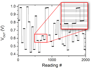
In an -bit RS-based MLC memory, one has to encode the memory levels as distinct resistance states. Thus, the memory states can be identified with each one of the consecutive and adjacent resistance “bins” of width , with . To store the memory state the device has to be “SET” to the corresponding bin, ie . The requirement of non-volatility implies that the value should remain within that bin, even after the input is disconnected or the memory state is read out. In Fig. 1 we plot data of a random sequence of stored memory states in our implementation of a 64-level (6-bit) MLC. For practical convenience resistance levels are translated into voltage levels by a fixed bias current.
The central component of the MLC is a RS device of a resistance , whose magnitude can be changed by application of a current pulse . The resistance change depends on through a highly non-trivial function ; The function is usually unknown, however, an important general requirement for non-volatile memory applications using RS is that for currents below a given threshold. This allows to sense (ie, read-out) a stored memory state, ie the so called remnant resistance , injecting a bias current without modifying the stored information. Thus, , . A two level memory can be simply implemented by pulsing a RS-device strongly with opposite polarities and sensing the corresponding high and low states with a weak bias current. However, the previous observation of a current threshold has an important consequence for the implementation of MLC memories. In fact, in order to implement an MLC one should be able to tune the value of to any desired value. The better the control on this tuning, the better the ability to define the “bins” and a larger number of bits could be coded in the MLC. In principle, a perfect knowledge of the function should allow for this, but in practice the function is not known. Yet, any reasonable form of would allow to tune any arbitrary memory state by applying a sequence of pulses of decreasing intensity, following a simple “zero-finding” algorithm as in standard control circuit. Nevertheless, the requirement of a threshold current difficult the fine tuning, as small corrections beneath have no effect. In practice, the dead-zone introduced by relatively large values of prevents a straightforward implementation of RS-device as MLC memories with a large number of levels. Below we shall demonstrate how this conceptual problem can be overcome, and exhibit the implementation of a 64-level MLC.
II Implementation
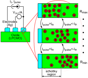
We adopt a manganite-based RS-device, made by depositing silver contacts on a sintered pellet of La0.325Pr0.3Ca0.375MnO3 (LPCMO) [15]. A RS-device is defined between the pulsed Ag/LPCMO and a second non-pulsed contact. A third electrode (earth) is required in a minimal 3-contact configuration setup.
A requirement for our MLC is that the RS-device operates in bipolar RS mode [1, 2, 3], ie, depending on the pulse polarity the remnant resistance either increases or decreases.
It is now well established that the mechanism behind bipolar RS is the redistribution of oxygen vacancies, within the nanometer-scale region of the sample in contact with the electrodes [2]. In the case of LPCMO, the oxygen vacancies significantly increase its resistivity because the electrical transport relies on the double-exchange mechanism mediated by the oxygen atoms [16].
Pulsing an electrical current trough the contact will produce a large electric field at the interface due to the high resistivity of the Ag/LPCMO Schottky barrier. If the pulse is strong enough, it will enable the migration oxygen ions across the barrier, modifying the concentration of vacancies and, hence, changing the interface resistance. The ionic migration remains always near the interface and does not penetrate deep into the bulk, since the much larger conductivity there prevents the development of high electric fields. Thus, the RS effect remains confined to a nanometer-sized region near the interface, as schematically depicted in Fig. 2.
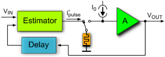
We now introduce a practical implementation of an RS-based MLC that produced the results shown in Fig. 1. We used an Ag/LPCMO interface and off-the-shelf electronic components. The block diagram of the concept is presented in Fig. 3 and the schematics and technical details are included in the Appendix. We envisage an implementation of an RS-based MLC memory chip where the storage core is a set of many RS-units with a single common control circuit. The common control would set each of the individual RS-units, one at a time, thus resembling the concept of the refresh logic circuit in the DRAMs. In this work we demonstrate the implementation of the control circuit with a single RS memory unit.
Key to our MLC implementation is to adopt a discrete-time algorithm that overcomes the problems discussed above [17], and which we describe next. The required memory state is coded in terms of a , while indicates the actual stored value (Fig. 3). The system iteratively applies pulses of a strength that is an estimate of the required value to set the target state , eventually converging to it. This discrete-time feedback loop continuously cycles between 2 stages; “probe” and “correct”. In probe stage the switch connects the RS-device to the current source in order to sense the remnant resistance. In the correct stage, the switch connects the RS-device to a pulse generator that applies a corrective pulse , of a strength that is obtained from the difference between the delayed and the target value as follows,
| (1) |
where the error signal is the change required in the output voltage and , being the frequency of the system clock and an integer. and are generic proportional and integral constants respectively with unit, being and the electric current and voltage units. The first term of the equation represents a proportional estimator. The second term prevents the system to get stuck in a condition where . In fact, for low a pulse of strength would lay below the threshold, thus not producing any further change in the state of the system. The magnitude of the second term linearly increases in time, thus making to eventually overcome the threshold and correct the output voltage in the desired direction.
Notice that even if this approach resembles a standard proportional-integral (PI) control loop with dead-zone, there are substantial differences. First, the remnant resistance reading and the correcting pulse application occur at different times. This requires the addition of the continuously commuting switch. Second, we also needed the introduction of a delay, implemented as a sample and hold circuit, as is required for the feedback path. These differences and the strong non-linearity in makes the stability analysis of this approach (which also depends on specific values of and ) a significant issue that we describe below.
III Stability analysis
III-A Discrete-Time Model
The study of the system stability is based on the discrete-time model presented in Fig. 4. In the z-domain, Eq. 1 becomes
| (2) |
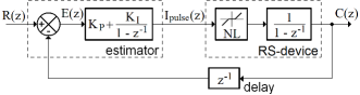
The resulting after these corrective pulses is probed by connecting the RS-device to the bias current source (), obtaining the output signal ( in z-domain). In the next cycle, it will be compared to the reference input generating the error signal . This fact implies the 1-cycle delay .
Central to the present proposal is the following equation, a discrete-time model for the RS-device:
| (3) |
where and , having resistance units, are an offset and a proportionality factor respectively. is a non-linear function that has to be defined on the basis of the general behavior of a RS-device operating in bipolar mode. In this model the is calculated by integrating the writing pulses after been weighted by the function. In this way, we model the possible change of the device resistance after the -th pulse as .
A concrete implementation of NL is presented below
| (4) |
The unit of is .When a negative signal exceeds the threshold , decreases as a linear function of with slope 1. For a positive signal greater than , increases with slope . For the sake of stability analysis Eq. 3 is simplified as:
| (5) |
In this way, the analysis is not considering any instability when sensing with . Indeed, our actual implementation did not present any critical issue at this level (see the Appendix). From now on, unit-step sequence is considered as input signal [18]. The steady-state error for the system with (just proportional control) and is , then the steady-state response is . In fact, Fig. 5(a) shows that the system converges to the required set-point only for . The system arrives to this condition because when the excitation of the RS-device is , i.e. lower than the minimum voltage required to produce a change in . A proportional control that enters into this condition, remains there indefinitely. The integral term in Eq. 2, that turns the system into a PI control, avoids the problem; when continuously integrated, makes to eventually overcome the threshold . See Fig. 5(b) and (c).
III-B Analysis without
We begin by considering the simplified situation where the stability is analyzed by removing the nonlinearities introduced by ( and ). The transfer function of the system is . For (typical value) the system is critically damped when , and remains stable for . Increasing moves the location of the poles following , arriving to when , where the system becomes unstable for any (see Fig. 5 (m)).
III-C Analysis with
Although the introduction of nonlinearities in Eq. 4 does not allow to study the system analytically, as in the previous section, its response might be numerically simulated. In fact, simulations where performed in the -space by solving Eq. 5, after substituting (Eq. 1) and (Eq. 4). For the computation of , we assigned and the unitary step function at the input (ie. ).
Fig. 5 (d-f) shows this simulated response of the system for three sets corresponding to representative position of the poles of the equivalent system without nonlinearities.
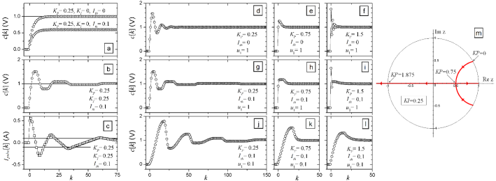
Fig. 5 (g-i) shows the effect of introducing the threshold () for the same set . The system response is qualitatively the same with the addition of periods where is “frozen” because , while the integral term is growing. Fig. 5 (j-l) shows the effect of further introducing asymmetry into the nonlinear function . The effect that this nonlinearity introduces when is equivalent to reducing the gain of the system for (see Eq. 4). In fact, Fig. 5(j) evidences a clear difference between the system speed when is increasing as compared to the speed when is decreasing. The case for is equivalent to a case where and .
Simulations also show a change in the stability limit as reported in the following table:
| stability limit () | ||
|---|---|---|
| 0 | 1 | |
| 0.1 | 1 | |
| 0.1 | 0.1 |
Summarizing, the simulations show that the system stability is not compromised after the introduction of nonlinearities, even if in some conditions, the system might require a considerably higher number of cycles to stabilize.
IV Results
Two tests were done to evaluate the performance of the MLC memory. Experimental results for the memory retention test are presented in Fig. 6. We emphasize that the relatively slow operation speed of our memory MLC would be dramatically improved upon device miniaturization and integration. For simplicity, we sampled a random subset of 16 out of 64 different voltages uniformly distributed along the operative range (Fig. 6(a)). Each write and read cycle had a duration of 13 seconds. In the first 5 s the WR signal was active and a memory value was SET. After a memory value was SET, we observed a small relaxation of with time constant of 1.6 s. The value of remained essentially stable afterwards. Thus, for the sake of performing a large number measurements, we only monitored the memory retentivity during the 5 time-constants (ie, 8 seconds) that immediately followed the SET. Within that period, the WR signal was inactive, and the memory state stored in was probed every 0.1 s (ie, the memory was read out 80 times).
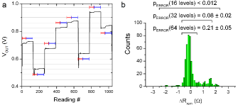
In Fig. 6(b) we present the histogram of the distribution of observed errors in the reading of a given stored memory value. The observed values correspond to the remnant resistance of the memory cell, after reading it 80 times at a 10 Hz rate, following the SET. The histogram is constructed from a sequence of 460 memory state recordings.
The finite dispersion of the histogram is the main limitation for implementing a high number of memory levels. To easily visualize the retentivity performance of the memory for increasing number of levels, we indicate with horizontal bars the resistance interval ( =) that corresponds to having a 16, 32 and 64 MLC memory (ie, 4, 5 and 6 bits, respectively). The probability of error in storing a memory state corresponds to the area of the histogram that lays outside the resistance interval normalized to the total area. With a confidence level of 95%, the probability that the MLC fails to retain a stored state is 0.210.05 for a 64-level system (6 bit MLC). This error probability rapidly improves as the number of levels is decreased, being 0.012 for a 16-level MLC.
The previous data on the performance of the memory can also be expressed in terms of the bit error rates (BER). In our MLC, we find BER0.006 for the 16-level system, BER0.07 for the 32-level system and BER0.1 for the 64-level system. Lower error probabilities for bits than for levels, reflects the fact that, typically, the error corresponds to the memory level drifting to an immediate neighbor level (that often shares a large number of bits).
V Conclusions
In conclusion, we have introduced a feedback algorithm to precisely set the remnant resistance of a RS-device to an arbitrary desired value within the device working range. This overcomes the conceptual problem of fine tuning a resistance value in non-volatile RS-devices for MLC applications, due the presence of a threshold current behavior. The feedback configuration is intrinsically time-discrete, since it is based on read / write sequences. The overhead in the writing time introduced in this feedback system may be a limitation for its utilization as primary memory in a computer system, but it can easily compete with actual speed of the current mass storage devices (flash memories). The applicability of the concept to implement an n-bit MLC memory was successfully demonstrated for = 4, 5 and 6, with an LPCMO-based circuit; which clearly illustrates the critical trade-off between BER, number of memory levels and (power and area) overhead of the control circuitry.
[Schematics and technical details of the circuit]
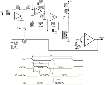
Fig. 7 shows a simplified circuit of our implementation. The “estimator” circuit (see Fig. 3 and Fig. 4) is implemented by IC100D, IC101A and the high-current buffer A3 (and associated components). It compares the output of the “sample and hold” (S&H) against the input signal divided by 2, and then computes the PI function. and are set by means of P101 and P100 respectively.
During the “correct” state, corrective pulses are applied to the RS-devices (LPCMO), by closing S1 during s. C102 and R109 introduce a time constant of s, reducing the rise time of the pulses in order to avoid overshoots. In the “probe” state, IC103B closes first and ms after, IC103A. Also, S4 clamps the inverting input of A3 to V+. The timing of the circuit is generated by a timing circuit based on the master clock CLK (see Fig. 7). A current flows trough the LPCMO (V+ = 7.5V, V- = -7.5V). The voltage drop at the switching interface of the RS-device (ranging 20-50 mV) is amplified by the instrumentation amplifier A1 (gain=21), eventually setting the voltage at the output of the S&H. Both interfaces of the RS-device behave complementary (ie. when one interface reduces its resistance, the other increases [2]), then the total drop across the device is 70 mV and quite insensitive to the state, and therefore, .
References
- [1] A. Sawa, “Resistive switching in transition metal oxides,” Materials Today, vol. 11, no. 6, pp. 28–36, 2008.
- [2] M. J. Rozenberg, M. J. Sánchez, R. Weht, C. Acha, F. Gomez-Marlasca, and P. Levy, “Mechanism for bipolar resistive switching in transition-metal oxides,” Phys. Rev. B, vol. 81, p. 115101, Mar 2010.
- [3] R. Waser, R. Dittmann, G. Staikov, and K. Szot, “Redox-Based Resistive Switching Memories - Nanoionic Mechanisms, Prospects, and Challenges,” Advanced Materials, vol. 21, no. 25-26, pp. 2632–2663, 2009.
- [4] D. B. Strukov, G. S. Snider, D. R. Stewart, and R. S. Williams, “The missing memristor found,” Nature, vol. 453, pp. 80–83, May 2008.
- [5] “International technology roadmap for semiconductors.” http://www.itrs.net/, 2011.
- [6] H. Lee, P. Chen, T. Wu, Y. Chen, C. Wang, P. Tzeng, C. Lin, F. Chen, C. Lien, and M. Tsai, “Low power and high speed bipolar switching with a thin reactive Ti buffer layer in robust HfO2 based RRAM,” in Electron Devices Meeting, 2008. IEDM 2008. IEEE International, pp. 1–4, IEEE, 2008.
- [7] A. Beck, J. G. Bednorz, C. Gerber, C. Rossel, and D. Widmer, “Reproducible switching effect in thin oxide films for memory applications,” Appl Phys Lett, vol. 77, no. 1, pp. 139–141, 2000.
- [8] F. Alibart, L. Gao, B. D. Hoskins, and D. B. Strukov, “High precision tuning of state for memristive devices by adaptable variation-tolerant algorithm,” Nanotechnology, vol. 23, no. 7, p. 075201, 2012.
- [9] H. Kim, M. P. Sah, C. Yang, and L. O. Chua, “Memristor-based multilevel memory,” in Proc. 12th Int Cellular Nanoscale Networks and Their Applications (CNNA) Workshop, pp. 1–6, 2010.
- [10] C. He, Z. Shi, L. Zhang, W. Yang, R. Yang, D. Shi, and G. Zhang, “Multilevel Resistive Switching in Planar Graphene/SiO2 Nanogap Structures,” ACS Nano, vol. 6, no. 5, pp. 4214–4221, 2012.
- [11] C. Schindler, S. Thermadam, R. Waser, and M. Kozicki, “Bipolar and Unipolar Resistive Switching in Cu-Doped SiO2,” Electron Devices, IEEE Transactions on, vol. 54, no. 10, pp. 2762–2768, 2007.
- [12] B. Ricco, G. Torelli, M. Lanzoni, A. Manstretta, H. E. Maes, D. Montanari, and A. Modelli, “Nonvolatile multilevel memories for digital applications,” vol. 86, no. 12, pp. 2399–2423, 1998.
- [13] S. Tanakamaru, C. Hung, and K. Takeuchi, “Highly Reliable and Low Power SSD Using Asymmetric Coding and Stripe Bitline-Pattern Elimination Programming,” vol. 47, no. 1, pp. 85–96, 2012.
- [14] N. Papandreou, H. Pozidis, A. Pantazi, A. Sebastian, M. Breitwisch, C. Lam, and E. Eleftheriou, “Programming algorithms for multilevel phase-change memory,” in Proc. IEEE Int Circuits and Systems (ISCAS) Symp, pp. 329–332, 2011.
- [15] N. Ghenzi, M. J. Sanchez, F. Gomez-Marlasca, P. Levy, and M. J. Rozenberg, “Hysteresis switching loops in Ag-manganite memristive interfaces,” J Appl Phys, vol. 107, no. 9, p. 093719, 2010.
- [16] E. Dagotto, Nanoscale Phase Separation and Colossal Magnetoresistance: The Physics of Manganites and Related Compounds. Springer Series in Solid-State Sciences, Springer, 2003.
- [17] K. Ogata, Discrete-Time Control Systems. Prentice Hall International editions, Prentice-Hall International, 1995.
- [18] C. Chen, Analog and Digital Control System Design: Transfer-Function, State-Space, and Algebraic Methods. Saunders College Publishing Electrical Engineering, Oxford University Press, USA, 1993.