Effect of Temperature and Charged Particle Fluence on the Resistivity of Polycrystalline CVD Diamond Sensors
Abstract
The resistivity of polycrystalline chemical vapor deposition diamond sensors is studied in samples exposed to fluences relevant to the environment of the High Luminosity Large Hadron Collider. We measure the leakage current for a range of bias voltages on samples irradiated with 800 MeV protons up to p/cm2. The proton beam at LANSCE, Los Alamos National Laboratory, was applied to irradiate the samples. The devices’ resistivity is extracted for temperatures in the C to C range.
1 Introduction
Polycrystalline chemical vapor deposition (CVD) diamond [1, 2, 3, 4] is presently used in particle physics experiments for beam monitoring [5, 6], and it is being further developed [7] for use in vertexing and tracking detectors planned for the challenging radiation environment of the inner layers of High Luminosity Large Hadron Collider (HL-LHC) detectors. At distances shorter than about 24 cm from an LHC collision (i.e., the regime covered by inner pixel detectors), the dominant source of radiation damage is charged particles. Any effect of radiation damage upon the resistivity of the detection material will, if uncompensated, propagate to the leakage current; the result would be that all assessments of the material properties that depend upon leakage current measurement, including active volume and charge collection distance, would be impacted. Accordingly we have studied the resistivity of polycrystalline CVD diamonds as a function of temperature and proton fluence. The 800 MeV proton beam at LANSCE, Los Alamos, was used in the irradiation. This study was carried out in the framework of the RD42 Collaboration at CERN.
2 Method
The devices (see Table 1), manufactured by Element Six [8], are polycrystalline and structured with metalized pads and backplane. The cleaning and metalization process is based on a technique in [9]. That process begins with application of three heavily oxidizing acids to remove all organic residues and leave the surface oxygen terminated. The sequence is HCl-HNO3 (3:1), H2SO4 (3:2), then H2SO4-H2O2 (1:1). This is followed by an oxygen plasma etch for 4 minutes. After the high energy sputter by composite TiW, the contacts are annealed for another 4 minutes at C in an inert atmosphere.
The device thicknesses were measured with an Eichhorn and Hausmann Contactless Wafer Thickness and Geometry Gauge (model MX 203-6-33) and confirmed optically with a microscope; their lengths and widths were measured optically. These diamonds are taken from the same series, number 1006115, produced in 2008. As the results from the two devices are consistent, for clarity the graphs in this paper display the 1006115-36 data unless otherwise indicated (these are indicated in the legends of the graphs as “15-36.”) Device 1006115-36 was exposed to fluences , , , and p/cm2. Device 1006115-46 (indicated in the graphs as “15-46”) was exposed to fluences and p/cm2.
| Diamond sensor | Dimensions (cmcmm) |
|---|---|
| 1006115-36 | |
| 1006115-46 |
Resistivity is computed as
| (1) |
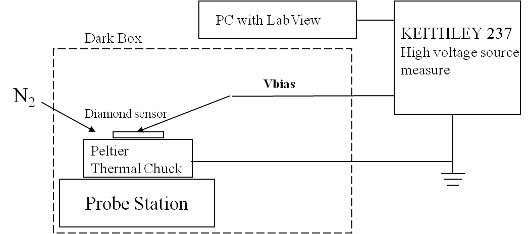
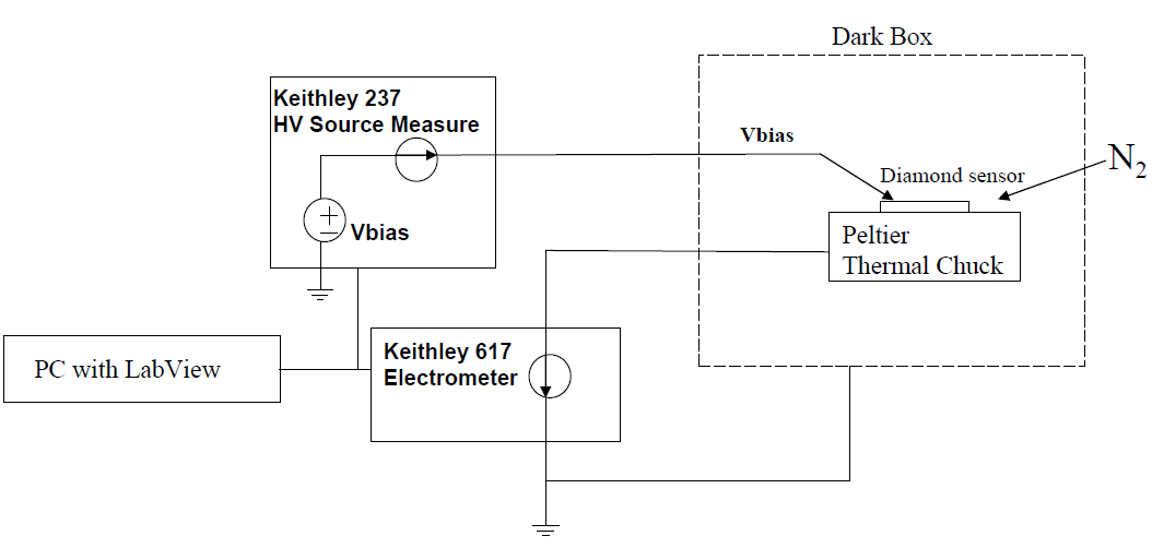
where is the inverse of the slope of a linear fit to a graph of leakage current versus bias voltage (“IV”); is the area of the sensor under test; and is the sensor thickness. Two slightly different setups, see Figure 1, were used for the IV measurement in order to quantify systematic uncertainty associated with the instrument configuration. With ground applied to the detector back side and high voltage applied to the front, the bulk leakage current data are acquired by the Keithley 237 source measure unit in Setup 1 and by the Keithley 617 electrometer in Setup 2. The advantage of Setup 1 is its simplicity: a single instrument is used to measure the sourced current. The advantage of Setup 2 is the fact that the measurement is made instead on the returned current (so sourced current that did not cross the bulk is excluded); the disadvantage is that this setup requires two instruments, each with its own intrinsic contribution to measurement uncertainty. Dry N2 is applied continuously to the environment to prevent condensation. The sensor temperature is maintained at approximately C, C, C or C by the thermal chuck on which the sensor rests. Relative humidity is less than 5% for all measurements below and less than 35% for room temperature measurements. Bias voltage is ramped over the range from -500 V to +500 V with confirmation measurements in both directions. Data taken with positive and negative voltage are fitted separately for voltages with magnitude of 200 V and higher. (We exclude data for voltages in the realm of 100 V, as these currents are comparable to the intrinsic accuracy of the Keithley devices which is 100 fA.) The separate fits are consistent, and the slope is their average.
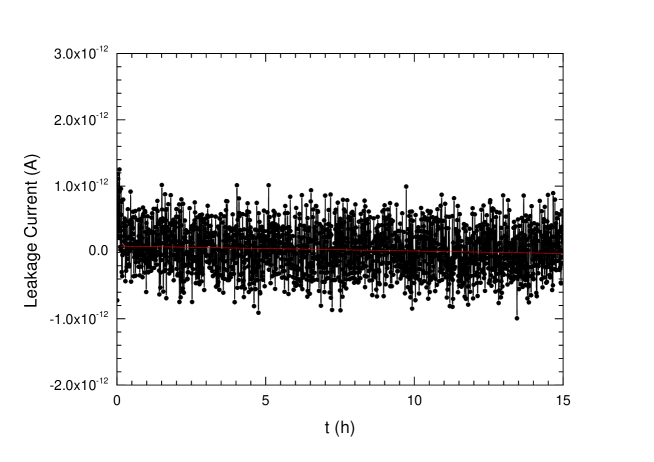
The standard deviation on any measured current varies between 3 and 9 A, depending upon the setup, derived from three to five measurements under identical conditions. The standard deviation is unaffected by the temperature or humidity within the ranges used here. An interval of a few hours is typically allocated to the measurement of a single IV point. After being mounted to the thermal chuck, the diamond’s current and temperature are monitored continuously. The temperature of the diamond is recorded through a thermal sensor mounted directly to the thermal chuck. Temperature uncertainty is less than C for any individual measurement and falls in the range to C for the full voltage scan of most devices. Equilibration takes approximately 30 minutes. An average current and temperature are extracted from data during the period beginning about one hour after installation and continuing up to four hours. We do not observe any deviations of the average slope from flatness during these intervals. Figure 2 demonstrates the stability of the current at a typical bias point and illustrates the size of a standard deviation on any measured current. That particular measurement involved application of 500 V over 15 hours at C to diamond 1006115-36 after it had received p/cm2. The line fitted to the graph for all data after 30 minutes intercepts current fA with slope of A/hr, i.e., consistent with zero. For the interval from 1 hr to 4 hr over which a measurement is taken, the slope of the data is A/hr.
3 Results
3.1 Leakage Current
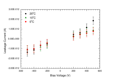
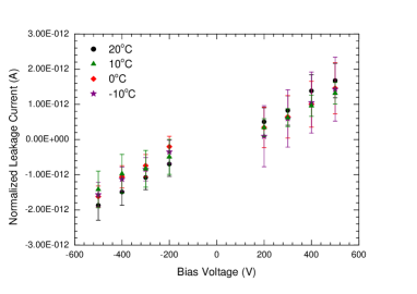
Figure 3 shows the leakage current in diamond 1006115-36 for positive and negative bias voltages up to 500 V. This diamond showed breakdown just above 500 V prior to irradiation, and that set the scale for our studies. After receiving fluences of and p/cm2, however, it was tested to 1000 V without breakdown. At fluence p/cm2, it again displayed breakdown just above 500 V. Diamond 1006115-46 similarly showed breakdown near 500 V before irradiation. After irradiation it was tested up to 800 V without breakdown.
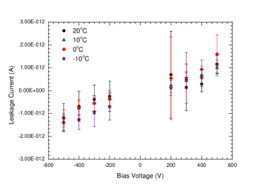
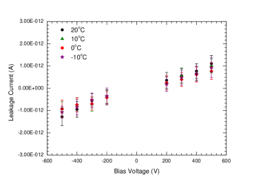
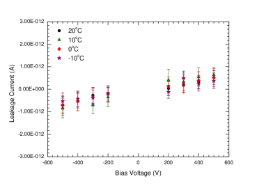
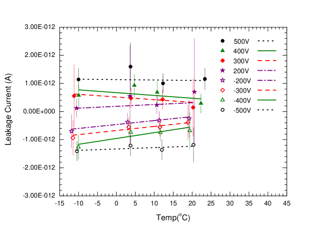
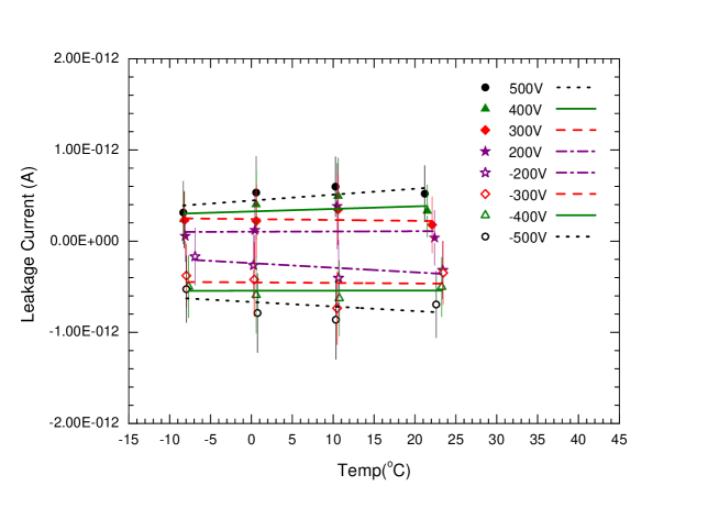
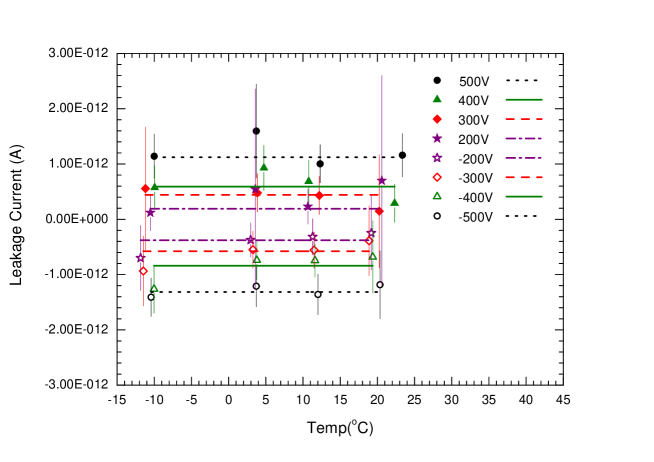
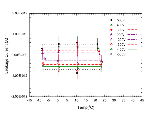
The IV characteristics are consistent for temperatures in the range to C for fluences up to p/cm2. (An instrument failure caused the data taken at C after the exposure to be lost.) We observe no dependence of leakage current upon temperature in this range: Figure 4 displays this information for two example fluences with straight-line fits, slope unconstrained, to the data. The values of /dof for the fits in Figure 4 range from 0.1 to 1.1. If the fits are redone for slopes fixed to zero (Figure 5), the range of /dof values is 0.1 to 1.5.
3.2 Resistivity
The data in each IV graph are fitted to straight lines for the two separate ranges [-500 V, -200 V] and [200 V, 500 V]. For each temperature and fluence combination, those two slopes are extracted and averaged, and this average is converted to a resistivity using Equation 1. To illustrate the method, Figure 6 shows the set of fitted lines resulting from this procedure applied to sensor 1006115-36 after exposure to 800 MeV protons/cm2.
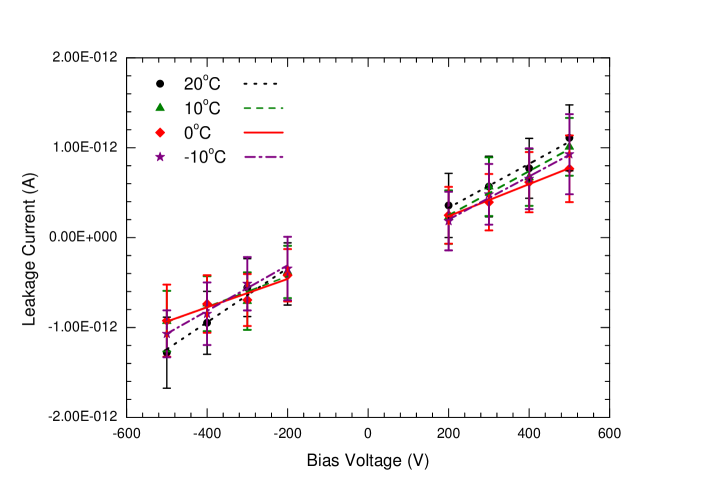
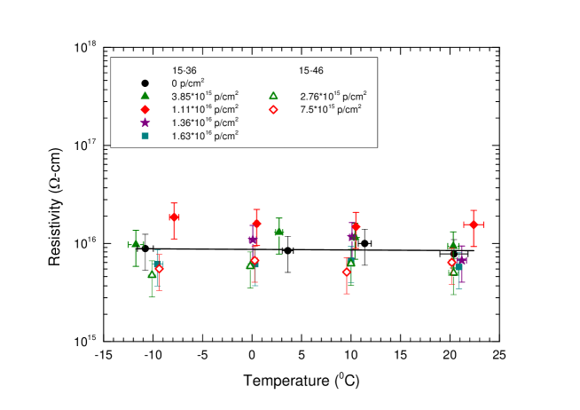
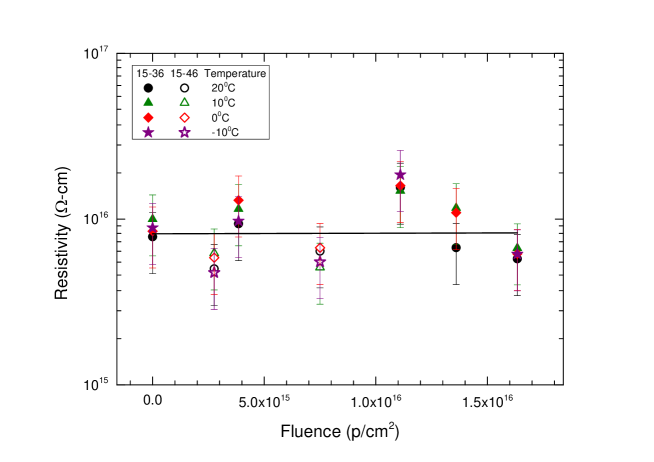
Figure 7 summarizes the resistivity versus temperature for all fluences and both diamonds. Figure 8 summarizes the resistivity versus fluence for all temperatures and both diamonds. The error bars on these graphs are the quadrature sum of statistical and systematic uncertainties (see below). A linear fit to the data in Figure 7 returns an intercept of -cm and slope -cm/∘C, with /dof 0.62. A linear fit to the data in Figure 8 returns an intercept of -cm and slope -cm/(p/cm2) with similar /dof. Thus diamond 1006115-36 and diamond 1006115-46 both have resistivity approximately Ohm-cm, independent of fluence up to 800-MeV p/cm2 and independent of temperature over the range [ C, C]. The propagated uncertainties on the resistivity of the diamonds range from 10 to 30% for 1006115-36 and 10 to 40% for 1006115-46. Setup 2 was used for the measurements of diamond 1006115-36 at fluence p/cm2 and temperatures C, C, and C and for the measurements of diamond 1006115-46 at fluences p/cm2 and p/cm2 and temperatures C, C, C, and . Setup 1 was used for the complement of the measurements. Measurements of diamond 1006115-36 at C after fluence p/cm2 were made with both setups.
3.3 Systematic Uncertainties
The systematic uncertainties on the bias voltage and leakage current derive from the manufacturer’s accuracy specifications for the Keithley 237 and 617 and are and fA) respectively. The uncertainties on the measured dimensions are given in the caption of Table 1. The fluences are known to 10-30%. The systematic uncertainty on the measured value of for each temperature and fluence condition is obtained by shifting the measured voltages standard deviation while shifting the measured currents standard deviation, then separately refitting the data in Figure 3. All of these contributions yield a systematic uncertainty of magnitude 1 to Ohm-cm, about one order of magnitude smaller than the statistical uncertainties. The systematic uncertainty associated with the setup configuration is 40%. This was determined experimentally by measuring a device with both setups under the same conditions. This uncertainty is traceable to the fact that in the current and temperature regime of this study, the intrinsic accuracy of the Keithley 617 (used in Setup 2) is 1.6% of the reading whereas the intrinsic accuracy of the Keithley 237 (used in Setup 1) is 0.3%.
4 Conclusions
The resistivity of chemical vapor deposition polycrystalline diamond sensors has been measured for samples irradiated with 800 MeV protons in several steps to a fluence of p/cm2. The measurements were made in a controlled-humidity environment over the temperature range approximately to C. We find no evidence for significant dependence of the resistivity upon either temperature or particle fluence within the ranges studied. The resistivity of two diamonds in the same series was found to be very consistent and of order of magnitude of Ohm-cm.
5 Acknowledgements
We thank Harris Kagan for providing the diamond sensors. This work was supported by the U.S. Department of Energy.
References
- [1] M. Marinelli, et al., “High-Quality Diamond Grown by Chemical-Vapor Deposition: Improved Charge Collection Efficiency in -Particle Detection,” Appl. Phys. Lett. vol. 75, no. 20 (1999) 3216-3218.
- [2] P.J. Sellin, et al., “Imaging of Charge Transport in Polycrystalline Diamond Using Ion-Beam-Induced Charge Microscopy,” Appl. Phys. Lett. vol. 77, no. 6 (2000) 913-915.
- [3] M. Schloegl and B.E. Fischer, “Investigation of the Detection Efficiency of Polycrystalline Diamond Detectors with a Heavy Ion Microprobe,” Proc. 1999 Fifth European Conf. on Radiation and its Effects on Components and Systems, Fontevraud, France (2000) 132-135.
- [4] A. Brambilla, et al., “Thin CVD Diamond Detectors With High Charge Collection Efficiency,” IEEE Trans. Nucl. Sci. vol. 49, no. 1 (2002) 277-280.
- [5] A. Gorisek, et al., “ATLAS Diamond Beam Condition Monitor,” Nucl. Instr. and Meth. A 572 (2007) 67-69.
- [6] E. Bartz et al., “The PLT: A Luminosity Monitor for CMS Based on Single-Crystal Diamond Pixel Sensors,” Nucl. Phys. B Proc. Suppl. 197 (2009) 171-174.
- [7] D. Asner et al., “Diamond Pixel Modules,” Nucl. Instr. and Meth. A 636 (2011) S125-S129.
- [8] www.e6.com.
- [9] S. Zhao, “Characterization of the Electrical Properties of Polycrystalline Diamond Films,” Ph.D. dissertation, The Ohio State University, 1994 (unpublished).