Influence of Dielectric Environment on Role of Spin-Orbit Interaction for Image Potentials
Abstract
We present a formalism for calculating the image potential for a two-dimensional electron gas (2DEG) with Rashba spin-orbit interaction (SOI) as well as for a 2D topological insulator (TI). The formalism is further generalized for including the Coulomb coupled multiple layers. Roles of broken inversion symmetry near the surface and the dielectric environment are investigated by using a surface-response function. The insignificant role of SOI in 2DEG is dramatically enhanced in TI by selecting a small relative permittivity for the dielectric environment. Manipulating is proven to provide an efficient way to drive electrons with opposite spins into two different integral quantum Hall states. The prediction made in this paper is expected to be experimentally observable for a 2DTI system, such as Bi2Se3, with a helical spin behavior and a dominant linear Rashba SOI-like term in the energy dispersion.
__
Keywords: Image potential; spin-orbit interaction; two-dimensional electron gas; topological insulator.
I Introduction
In recent times, there has been a considerable amount of research studies on the role played by the Rashba rashba spin-orbit interaction (SOI) on the collective-excitation properties of the two-dimensional electron gas (2DEG) formed in a semiconductor heterostructure. Special focus was placed on its affluence of plasma excitations gg ; manvir1 ; manvir2 ; wenxu ; 1 ; 2 ; 3 ; exact1 ; exact2 and electron transport 3 . It has been predicted theoretically that plasmon propagation becomes tunable in the presence of an external electric field via SOI. This provides a way for transmitting quantum information in a quantum device and opens up a new possibility for the so-called plasmon-field effect transistor. Experimentalists are specifically interested in exploiting the Rashba SOI in InAs or InGaAs so as to gain control over the spin population by increasing a lateral or gate field and then pumping electrons. There were some papers M1 ; M2 ; M3 ; M4 ; M5 on ballistic quantization in InAs, even though the mobility was much less than GaAs. However, in a theoreti cal study, we found that SOI plays a significant role in the conductance quantization of quantum wires dh1 ; dh2 .
In Refs. [exact1, ; exact2, ], the authors evaluated charge and spin density response functions gg of a 2DEG with Rashba spin-orbit coupling at finite momenta and frequencies. The polarization function is the basis for calculating the plasmon dispersion and the quasi-classical approximations. Additionally, one can employ the polarization function to obtain the surface-response function which is a crucial ingredient in the analysis of the electronic properties of single and Coulomb coupled 2DEG layers book .
Here, we investigated the effect of the Rashba SOI on the image potential for a single-layer 2DEG as well as for two layers which are Coulomb coupled. Using the static limit for the surface-response function with and without SOI calculated self-consistently, we were able to analyze the role played by adjoining dielectric media on the image potential. In 2DEG, the linear- (in-plane wave vector) term (hereafter referred as Rashba term) lifts the spin degeneracy of the dispersion away from . But it only serves as a small perturbation to the dominant quadratic mass term . In 2D topological insulators (TIs) Science , such as Bi2Se3, their roles are inverted, that is, the Rashba term dominates the dispersion providing helical flavor to the topological conductance and valence surface states. This type of helical behavior also occurs in conventional 2DEG with SOI due to broken inversion symmetry near the sample surface. We compare the image potentials of both 2DEG and TI when the dielectric environment is varied. Related image-potentials for the semi-infinite metal/vacuum interface as well as for graphene have been studied 17 ; image1 ; image2 . Recently, the image states have been observed in pyrolytic graphite 18 and metal supported graphene 19 . We analyze how the SOI and the strong interlayer Coulomb coupling affect the image states. The image states for the double layer are formed through the interlayer hybridization of the image-potential state in individual 2DEG layer. The situation may be compared with that of double-layer graphene 4+ .
If a stationary external change, i.e. having velocity , is introduced to our two-dimensional electronic systems, we need only consider the static limit with , where is the wave vector of an induced collective excitation of the electron gas. Therefore, we can neglect the force contribution from the change of a vector potential with time and simply assume a zero Lorentz force for the external charge. As indicated previously mop , there exists a magnetoelectric polarizability associated with 3D topological insulators due to the so-called axion electrodynamics. As a result of this, the displacement field will also depends on the magnetic field, and the magnetic field in turn depends on the electric field as well. However, Poisson’s equation for the scalar potential still holds if we select the Coulomb gauge for our system. Additionally, the equation for the vector potential will maintain its form if the material considered is non-magnetic. In this sense, the image potential for the two-dimensional electron gas and topological insulator models discussed in Sec. II is well defined.
In addition, the image states of metallic carbon nanotubes 7 and double-wall non-metallic nanotubes 8 ; 8b were investigated. Experimental work 8c includes photoionization 8c+ and time-resolved photoimaging of image-potential states in carbon nanotubes 8cc+ . There has been general interest 8c++ in these structures because of electronic control on the nanoscale using image states. This has led to wide-ranging potential applications including field ionization of cold atoms near carbon nanotubes 8d , and chemisorption of fluorine atoms on the surface of carbon nanotubes 8e . We anticipate that the image states we investigate would lead to the experimental study of spin-orbit effects on electronic control devices, for example. Furthermore, the significance of the role played by the image-potential should become pronounced under suitable conditions which are discussed in the present paper.
In the rest of the paper, we first derive a formalism in Sec. II for calculating the image potential by a point charge in terms of a surface-response function. The surface-response function is further related to a single-particle density-density response function for both single- and double-layer systems. In Sec. III, the density-density response function is calculated explicitly for both 2DEG and TI systems. The numerical results for image potentials are compared in Sec. IV for both single- and double-layer 2DEG and TI as well embedded in different dielectric environments and with or without a Rashba SOI term. Finally, a brief conclusion is drawn in Sec. V with a remark.
II The image potential formalism
Consider a stationary external point charge located at with on the polar axis in vacuum. We assume that there is a material with background dielectric constant in the region . The external potential at r due to the presence of such a point charge can be obtained by solving Poisson’s equation
| (1) |
where the standard units is adopted with denoting the permittivity of free space. For , we obtain from Eq. (1)
| (2) |
Also, for , the induced potential is given by
| (3) |
where is the static surface-response function to be determined. Therefore, the force exerted on the external charge due to the induced charge in the medium is given by
| (4) | |||||
The relation in Eq. (4) defines the image potential as
| (5) | |||||
If we assume that there is a layer of 2DEG at and a second layer at distance from the first with material having dielectric constant between but vacuum for and , then the dynamical surface-response function for this double layer is given by
| (6) |
where and is the single-particle density-density response function.
In the limit of , we obtain the surface response from Eq. (6) for a single layer as
| (7) |
which was previously derived in the paper by Persson bnj . We find that if we replace the vacuum regions in our calculations above by a material with background dielectric constant and the material between the double layers by a material with background dielectric constant , then the corresponding surface-response function would still be given by Eq. (6), but with defined as the ratio of the two dielectric constants, i.e., . This then allows us to vary the nature of the dielectric environment to study the corresponding effect on the image potential.
To proceed further with our calculations, we need to calculate the polarization function. A natural first step in this direction is the energy eigenstates which we turn to in Sec. III. However, if we neglect the effect from the density-density response on the surface-response function (i.e. by taking ), the image potential (in units of with Rashba parameter and electron density ) for single and double layer configurations can be simply calculated as
| (8) | |||||
where is a hypergeometric function and is in units of .
III The Polarization Function
For a noninteracting ideal 2D electron or heavy hole (HH) gas in the -plane with SO coupling, the single-particle Hamiltonian is well known rashba . In fact, for a given spin, the Hamiltonian leads to a momentum-dependent force on the electron/hole, somewhat like a magnetic field. Moreover, the spin-dependence means that the time-reversal symmetry of SO coupling is different from a real magnetic field. For this case we can write down the Hamiltonian as
| (9) |
where is the effective mass of an electron or HH, , . In addition, is the Rashba parameter for an electron or HH system with for electrons and for HHs. The energy eigenvalues for the Hamiltonian in Eq. (9) are, in terms of an in-plane wave vector , given by
| (10) |
showing Dirac dispersion and helical spin texture, with eigenfunctions
| (11) |
where and is a normalization area. Also, for a chosen total electron () or hole () density, the spin “” or spin “” carriers will be distributed between the two sub-bands with density determined by
| (12) |
where for electrons and for HHs, for electrons and for HHs. Both and must be less than to ensure the validity of Eq. (12). If , then only the spin-“” sub-band is occupied. In such a model, electron spin is conserved, and there exists a spin current. An applied electrical field causes oppositely directed Hall currents with ‘+’ and ‘’ spins, respectively. The net charge current is zero, while the net spin current is nonzero, and even becomes quantized. However, in real solids there is no conserved direction of spin. Consequently, it is expected that /+ and / would always mix and the effect arising from the edge will be canceled out. The model state in this theory is just two copies of the integer quantum Hall (IQH) state. It was shown by Kane and Mele Kane-Mele that, in real solids with all spins mixed and a zero net spin current, only some part of physics outcome in this model can survive. Kane and Mele Kane-Mele further found a new topological invariant in time-reversal-invariant systems of fermions.
It is known that there exists a surface state, called a “holographic metal”, in Bi2Se3 family materials, where the surface state is 2D but still determined by the 3D bulk topological property. Such surface states can exist only in the range from to before their merging with (quadratic) bulk states and paring with surface states of the other boundary. Therefore, the number of Fermi-surface crossing for a single Kramers partner at one surface can be an odd integer, which is different from an even integer in a 1D time-reversal invariant system.
| (13) |
where the first term is related to quadratic bulk states, is the unit matrix and are the Pauli matrices. The parameters are phenomenological, taken from experiment and their values are indicated in the text. The parameters are specific for the material and can be calculated from the four-band tight-binding model (See Liu, et al., in Ref. [liu2010model, ]). We also present them in the text for . The similarity between the surface TI Hamiltonian and that for SOI was indicated in Ref. [liu2010model, ]. The model of Bernevig, Hughes and Zhang BHZ has been widely used for the TI description. Of course, one is justified in noticing the even (SOI) and odd (TI) number of dispersion crossing points with the Fermi surface. This arises from the dominantly quadratic term in the case of the SOI compared with the mostly linear TI dispersion. That is, for TIs, the quadratic part merges with the bulk valence band and is subsumed. In the model Hamiltonian, this property is of course not apparent. However, in the derivation of the polarization function (See Pletyukhov, et al., in Ref. [exact2, ]), a cut-off function for the wave vector was introduced. The value of the cut-off is much smaller than the crossing point where the quadratic part creates a non-physical crossing point. Therefore, there is no error introduced by those possible excitations. Consequently, in some way, the odd number of crossing points has to be built into the degree of accuracy for calculating the polarization function. From a mathematical point of view, the crossing points are and , where the Rashba wave vector is in Eq. (2) of Ref. [exact2, ]. The cut-off in Eq. (10) of Ref. [exact2, ] is . The first branch cut-off is much less than so that our method of calculation is reasonable. But, the second branch which is unphysical for TI must be removed so that it does not contribute numerically to the static polarization function.
It is interesting to note that the Hamiltonian describing surface states for Bi2Se3 TI may also be formally written in the form given by Eq. (9) with energy eigenvalues in Eq. (10) for topological surface states rashba ; winkler2003 . Consequently, we shall refer to the linear term in the energy dispersion as a Rashba-like term for TIs. As a matter of fact, for the TI with the material parameters liu2010model , , eVÅ, eVÅ2, eVÅ2, we get an effective mass where is the free electron mass. The Rashba-like parameter is given by . The above parameters were confirmed by ab initio calculations zhang2010first and experimentally verified via spin-resolved photo-emission spectroscopy (SRPES) hsieh2009tunable . Note that the sign of is determined by underlying atomic SOI.
The interplay between the two quantities, i.e. and , indicates that the Rashba-like term in TI is dominant in contrast with conventional 2DEG. As a result, the surface states show almost linear dispersion with helical spin structure, which has the opposite direction for the conduction and valence bands. Such helical structure is also characteristic for conventional 2DEG with SOI and arises from broken inversion symmetry near the sample surface. This symmetry breaking also manifest itself in the electron density distribution, as given by Eq. (12).
The linear screening of an external potential by the 2DEG (or TI surface states) embedded in a medium with background dielectric constant is given by
| (14) |
where the inverse dielectric function is expressed in terms of the density-density response function through
| (15) | |||||
In the self-consistent-field theory, the dielectric function takes in the form of , where the dynamic polarization function is given by
| (16) | |||||
is the Fermi function for electrons in a thermal-equilibrium state and is the angle between the wave vectors and . It is convenient to make double transformation , in the second term of Eq. (16). In the calculation for image potentials, we only require the static polarization function . For zero temperature regime it leads to:
| (17) | |||
Here, are the cut-off functions for the intra- and inter-band excitations. It is convenient to take it in the form of Gaussian:
| (18) |
with and being defined in the next section. Numerical simulations of the next section show that the polarization does not change perceptibly for the adjustable parameter to be in the range .
IV Numerical Results and Discussion
In this section, we first introduce unitless quantities:
| (19) |
where is the electron effective mass, is the surface electron density, is the Rashba parameter, is the Wigner-Seitz radius which is the ratio of the average inter-electron Coulomb interaction to the Fermi energy . In terms of these variables, we can rewrite appearing in Eqs. (6) and (7) in its unitless form: . Here, the static polarization function obtained from Eq. (16) with is given by the closed-form analytic expressions. Following the same procedure as in Ref. [exact2, ] and setting the cut-off functions for 2DEG with SO we obtain:
| (20) | |||||
where we have used and .
For the TI the Fermi energy crosses the dispersion curves in odd number of points, unlike for 2DEG with SO where the number of crossing points is even. Therefore there are no intraband excitations for . This can be modeled by the cut-off function in Eq. (18).
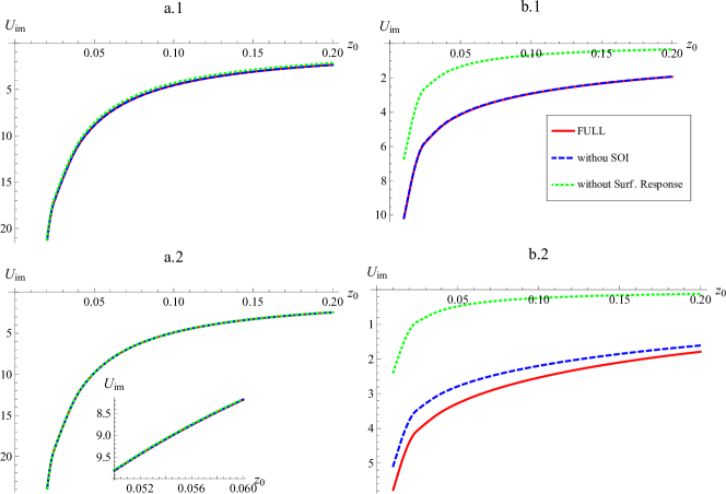
The necessary condition for showing SOI effect on image potential is a large Rashba parameter and a strong effect from a density-density response function, i.e., becomes comparable to . In Fig. 1, we plotted the image potential as a function of for the single-layer 2DEG and TI. In addition, in Fig. 2, we present results for 2DEG and TI with a double-layer structure and a layer separation Å. We have used Eq. (20) in the calculation of required in the surface-response function as well as the following numerical parameters. The electron density is cm-2. We chose the background dielectric constant appropriate for GaAs/AlGaAs as for the 2DEG, and for the TI (Be2Se3). The remaining parameters used in our calculations are as follows. For the 2DEG: and the Wigner-Seitz cell parameter . For the TI: and .
For these chosen values, our calculations have discovered that there is no difference for the image potential with/without the Rashba SOI for either the single-layer or the double-layer TI and 2DEG (with Å) when the ratio of the background dielectric constants for the materials on either side of the layers is large (i.e., for the 2DEG and for the TI) and the point charge is placed in the region with a smaller dielectric constant. It is clear from Eq. (7) that the surface-response function for the single-layer case (with ) approaches unity as and . As a result, no effect from SOI, which is included in the density-density response function, should be seen. For the double-layer case, the surface-response function in Eq. (6) does deviate from unity as long as is met. However, still holds, implying no visible SOI effect. In this case, the long-range part of the inter-layer Coulomb interaction dominates the density-density response function, leading to a spin-independent contribution to the image potential. When is assumed, we find from two panels (b.1) of Figs. 1 and 2 for 2DEG that the effect of surface-response function is greatly enhanced although the SOI effect is still invisible due to small Rashba parameter involved for the 2DEG. However, the SOI effect for TI becomes much more significant as can be seen from two panels (b.2) of Figs. 1 and 2 due to a much larger Rashba-like parameter involved for the TI. Consequently, the effect of SOI may be manipulated by adjusting the dielectric environment. For example, for the TI with a Rashba-like term to be comparable with the quadratic term in the energy dispersion due to a large value for , Fig. 2 demonstrates a spin-dependent sign switching with decreasing for the double-layer TI system.
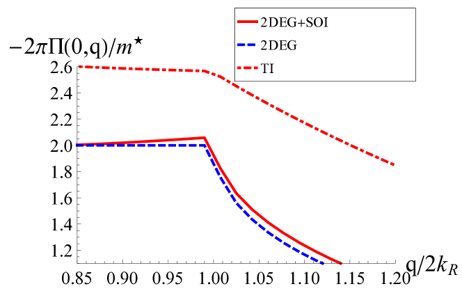
From the single-layer result presented in Fig. 1 we find that the effect of surface response function becomes significant for small values of . In addition, the SOI effect is more important for TIs than for 2DEGs. For the double-layer result displayed in Fig. 2, we further observe that the inter-layer Coulomb interaction can enhance the the effect of surface response function and change the sign of image potential from negative to positive. Again, the SOI effect is seen much more significant in TIs, where the SOI effect is contained within the static density-density response function and is independent of the layer separation. The higher the value is, the larger the asymmetry of the dielectric environment will be. Physically, the low values of implies a robustness of the system to an induced depolarization field by the Coulomb field from an external point charge. This mechanism is reflected in the calculated surface response function. For double-layer 2DEG/TI systems, the capability of the system to screen the depolarization field produced by the external point charge is further enhanced due to the existence of additional inter-layer Coulomb coupling. In order to see the role of static density-density response function, we compare in Fig. 3 the required static polarization function determined from Eq. (20) as a function of for the 2DEG in the presence and absence of the linear Rashba term. For comparison, we also plotted for the TI with a built-in Rashba-like linear term. The polarization function assumes a universal form for single layer 2DEG and TI. The SOI effect on the polarization function of the 2DEG is only enlarging it slightly. This minor enhancement becomes somewhat stronger as is increased. Such an enhancement is also accompanied by an upward shift in the plasmon frequency in the long wavelength limit for a 2DEG when SO coupling is included gg . For TI, on the other hand, becomes much stronger due to a large Rashba-like parameter. Furthermore, the difference in the static polarization function becomes pronounced for the image potential when the dielectric environment is adjusted as we described above.

V Concluding Remarks
In this paper, we considered a point charge placed above a 2D conducting layer at the interface between two dielectric media with relative permittivity . We have found from our study that the role played by the SOI on the image potential may be modified by varying . It has been shown that the SOI makes a nontrivial difference when the relative permittivity between the two dielectric media is reduced, thereby effectively separating the spin-‘’ (+) and spin-‘ ’ () electrons into different IQH states. Electron spin is conserved in this case, but there is still a spin current. The applied electric field due to the external point charge induces oppositely directed Hall currents associated with ‘+’ and ‘’-spins, respectively. Although the net charge current is zero, the net spin current is finite. The whole system becomes conducting due to the metallic nature of the sample edges. This net spin current, however, does not significantly affect the image potential of 2DEGs in our model. In the work of Kane and Mele Kane-Mele , it was shown that, in real solids when all spins mixed, there is no net spin current. It was further found that there exists a new topological invariant in time-reversal-invariant systems of fermions. As a matter of fact, a topological phase is insulating but always has metallic edges/surfaces when the sample is put next to vacuum or an ordinary phase. These considerations motivated us to explore the 2DEG with SOI as well as the 2D topological insulator using our formalism. Interestingly, for the TI the role played by the helical linear energy dispersion on the image potential is dramatically enhanced, in comparison with 2DEG. This occurs when the relative permittivity of adjoined media is reduced.
Acknowledgments
This research was supported by contract # FA 9453-11-01-0263 of AFRL. DH would like to thank the Air Force Office of Scientific Research (AFOSR) for its support.
References
- (1) Yu A. Bychkov and E. I. Rashba, J. Phys. C: Solid State Phys. 17, 6039 (1984).
- (2) G. Gumbs, Phys. Rev. B 72, 165351 (2005).
- (3) M. S. Kushwaha, Phys. Rev. B 74, 045304 (2006).
- (4) M. S. Kushwaha and S. E. Ulloa, Phys. Rev. B 73, 205306 (2006).
- (5) W. Xu, Appl. Phys. Lett. 82, 724 (2003).
- (6) M. K. Tahir and K. Sabeeh, Physica E 42, 1915 (2010).
- (7) S. M. Badalyan, A. Matos-Abiague, G. Vignale and J. Fabian, Phys. Rev. B 79, 205305 (2009).
- (8) C. Li and X. G. Wu, Appl. Phys. Lett. 93, 251501 (2008).
- (9) M. Pletyukhov and S. Konschuh, Eur. Phys. J. B 60, 29 (2007).
- (10) M. Pletyukhov and V. Gritsev, Phys. Rev. B 74, 045307 (2006).
- (11) G. Grabecki, J. Wróbel, T. Dietl, E. Janik, M. Aleszkiewicz, E. Papis, E. Kamińska, A. Piotrowska, G. Springholz and G. Bauer, Phys. Rev. B 72, 125332 (2005).
- (12) S. J. Koester, C. R. Bolognesi, M. J. Rooks, E. L. Hu and H. Kroemer, Appl. Phys. Lett. 99, 243114 (2011).
- (13) S. J. Koester, C. R. Bolognesi, E. L. Hu, H. Kroemer and M. J. Rooks, Phys. Rev. B 49, 8514 (1994).
- (14) S. J. Koester, C. R. Bolognesi, M. Thomas, E. L. Hu and H. Kroemer, Phys. Rev. B 50, 5710 (1994).
- (15) S. J. Koester, B. Brar, C. R. Bolognesi, E. J. Caine, A. Patlach, E. L. Hu, H. Kroemer and M. J. Rooks, Phys. Rev. B 53 13063 (1996).
- (16) G. Gumbs, A. Balassis and D. H. Huang, J. Appl. Phys. 108, 093704 (2010).
- (17) G. Gumbs, A. Balassis, D. H. Huang, S. Ahmed and R. Brennan, J. Appl. Phys. 110, 073709 (2011).
- (18) G. Gumbs and D. H. Huang, Properties of Interacting Low-Dimensional Systems (Wiley-VCH, Weinheim, Germany, 2011), pp. 275, 303.
- (19) X.-L. Qi, R. Li, J. Zang and S.-C. Zhang, Sci. 323, 1184 (2009).
- (20) P. M. Echenique and J. B. Pendry, J. Phys.: Condens. Matt. 11, 2065 (1978).
- (21) G. Gumbs, D. H. Huang and P. M. Echenique, Phys. Rev. B 79, 035410 (2009).
- (22) V. M. Silkin, J. Zhao, F. Guinea, E. V. Chulkov, P. M. Echenique and H. Petek, Phys. Rev. B 80, 121408(R) (2009).
- (23) J. Lehmann, M. Merschdorf, A. Thon, S. Voll and W. Pfeiffer, Phys. Rev. B 60, 17037 (1999).
- (24) I. Kinoshita, D. Ino, K. Nagata, K. Watanabe, N. Takagi and Y. Matsumoto, Phys. Rev. B 65, 241402(R) (2002).
- (25) M. Posternak, A. Baldereschi, A. J. Freeman, E. Wimmer and M. Weinert, Phys. Rev. Lett. 50, 761 (1983).
- (26) A. M. Essin, J. E. Moore and D. Vanderbilt, Phys. Rev. Lett. 102, 146805 (2009).
- (27) B. E. Granger, P. Král, H. R. Sadeghpour and M. Shapiro, Phys. Rev. Lett. 89, 135506 (2002).
- (28) G. Gumbs, A. Balassis and P. Fekete, Phys. Rev. B 73, 075411 (2006).
- (29) S. Segui, C. Celedon L pez, G. A. Bocan, J. L. Gervasoni and N. R. Arista, Phys. Rev. B 85, 235441 (2012).
- (30) K. Schouteden, A. Volodin, D. A. Muzychenko, M. P. Chowdhury, A. Fonseca, J. B. Nagy and C. Van Haesendonck, Nanotechn. 21, 485401 (2010).
- (31) M. A. McCune, M. E. Madjet and H. S. Chakraborty, J. Phys. B: At. Mol. Opt. Phys. 41, 201003 (2008).
- (32) M. Zamkov, N. Woody, S. Bing, H. S. Chakraborty, Z. Chang, U. Thumm and P. Richard, Phys. Rev. Lett. 93, 156803 (2004).
- (33) S. Segui, G. A. Bocan, N. R. Arista and J. L. Gervasoni, J. Phys.: Conference Series 194, 132013 (2009).
- (34) A. Goodsell, T. Ristroph, J. A. Golovchenko and L. V. Hau, Phys. Rev. Lett. 104, 133002 (2010).
- (35) V. L. A. Margulis and E. E. Muryumin, Physica B: Condensed Matter 390, 134 (2007).
- (36) B. N. J. Persson, Sol. State Commun. 52, 811 (1984).
- (37) C. L. Kane and E. J. Mele, Phys. Rev. Lett. 95, 146802 (2005).
- (38) C. X. Liu, X. L. Qi, H. J. Zhang, X. Dai, Z. Fang and S.-C. Zhang, Phys. Rev. B 82, 045122 (2010).
- (39) B. A. Bernevig, T. L. Hughes and S. C. Zhang Sci. 314, 1757 (2006).
- (40) K. Winkler, Spin-orbit coupling effects in two-dimentional electron and hole systems (Springer, Tracts in Modern Physics, 2003).
- (41) W. Zhang, R. Yu, R. H. J. Zhang, X. Dai and Z. Fang, New J. Phys. 12, 065013 (2010).
- (42) D. Hsieh, Y. Xia, D. Qian, L. Wray, L. J. H. Dil, F. Meier, J. Osterwalder, L. Patthey, J. G. Checkelsky, N. P. Ong, A. V. Fedorov, H. Lin, A. Bansil, D. Grauer, Y. S. Hor, R. J. Cava and M. Z. Hasan, Nat. 460, 1101 (2009).