Comparison of Fast Amplifiers for Diamond Detectors.
Abstract
The development of Chemical Vapour Deposition (CVD) diamond detectors requests for novel signal amplifiers, capable to match the superb signal-to-noise ratio and timing response of these detectors. Existing amplifiers are still far away from this goal and are the dominant contributors to the overall system noise and the main source of degradation of the energy and timing resolution. We tested a number of commercial amplifiers designed for diamond detector readout to identify the best solution for a particular application. This application required a deposited energy threshold below 100 keV and timing resolution of the order of 200 ps at 200 keV. None of tested amplifiers satisfies these requirements. The best solution to such application found to be the Cividec C6 amplifier, which allows 100 keV minimal threshold, but its coincidence timing resolution at 200 keV is as large as 1.2 ns.
I Introduction
Recent progress in the growth of Chemical Vapour Deposition (CVD) diamonds is challenging readout electronics developers. Because of its large bandgap of 5.5 eV and very low Boron and Nitrogen impurity concentrations 1-5 ppb E6 CVD diamond has a negligible intrinsic noise at room temperature. In fact, the mean leakage current of a typical device is less than 1 pA. Combining this with a very high carrier mobility of about c/(V/m), allowing for a complete charge collection in few ns (8 ns for 500 m thick device biased at 1 V/m), results in an intrinsic noise charge collected within the duration of the signal of the order of 0.05 electrons. Except for very slow, cryogenic, charge sensitive amplifiers, able to reduce the RMS noise to a few electrons, such precision is out of reach of modern fast amplifiers. Indeed, the best broadband amplifiers have input referred noise RMS of electrons corresponding to the input referred noise of 10 V (50 input impedance) in 8 ns signal. Even conventional charge amplifiers with 50-300 s decay time have more than 200 electrons RMS noise. Therefore, for diamond detector applications the dominant (by three-five orders of magnitude) source of noise is the readout electronics.
In the present note we present a series of tests on various fast amplifiers aimed to identify the best solution for nuclear and particle physics applications. These applications demand a measurement of both the energy released in the bulk of the diamond by ionizing particles and the time. These tests were performed using various radioactive sources.
II Experimental Setup
We selected a 4.7 x 4.7mm2, 500 um thick single crystal CVD diamond detector capacitance can be estimated according TO the plain
We selected 4.74.7 mm2, 500 m thick single crystal CVD diamond detector produced by Diamond Detectors Ltd DDL . The crystal has two electrodes deposited on its upper and lower major surfaces, made of few nm of DLC followed by 100 nm of Gold. Each contact is bonded via a gold microwire onto PCB and then to its SMA connector in such a way that both contacts can be read out independently. Detector capacitance can be estimated according to the plane capacitor equation (neglecting eventual fringe field contribution):
| (1) |
This result is in good agreement with the value measured by HP 4280A capacimeter.
The diamond detector was polarized at 1 V/m by means of Ortec 710 Bias Supply. This value remains below detector breakdown voltage (at 1.4 V/m discharges, likely to be attributed to crystal defects or contact disuniformity, occur) allowing for complete charge collection kagan .
In the present work, we used two types of readout: one-side readout, shown in Fig. 1 and two-side readout, shown in Fig. 2. The one-side readout was used to characterize energy resolution of of various amplifiers. In this case the diamond was polarized by applying 1 V/m bias voltage from the readout side and the other contact was connected to ground.
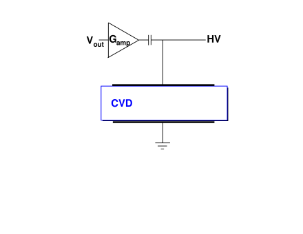
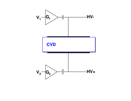
The two-side readout was used to study ideal timing resolution of the CVD diamond detector. Indeed, the major contribution to both energy and timing resolutions come from the readout electronics and in particular from the first amplification stage. Using the same diamond detector signal read out independently from opposite sides by two separate amplifiers allows to study the electronic contribution to the timing resolution using realistic signals.
For single amplifier characterization measurements the diamond detector was connected to the amplifier input through a 2.4 cm Huber & Suhner SMA “I” connector, while the second SMA connector of the detector was shorted to ground by SMA tap. The overall capacitance of the system in front of the amplifier (“I” connector, two SMA connectors of detector case and SMA tap) was found to be 6.6 pF.
The amplifier output was connected to the digitizer via 1.5 m Huber & Suhner SucoFlex 104 cable. The amplified signal was read out by SIS3305 digitizer with analog bandwidth of 2.2 GHz. The digitizer was operated in four-channel interleaved 5 Gs/s mode. For timing response measurements with small signals an additional amplifier Philips Scientific 744 with bandwidth of 1.8 GHz and gain was inserted between primary amplifier output and digitizer input.
The data measured by the digitizer was acquired through the VME bus by Concurrent Technologies VX 813/091 Single Board Computer (SBC) which incorporates a Tsi148 VME controller. A simple DAQ program was developed using DMA transfer of digitizer memory to the SBC memory. The data were saved on the local Compact Flash disk and transferred to workstation for the off-line analysis.
III Coincidence Trigger
In order to measure coincidence events and to reduce accessible energy threshold the standard SIS3305 digitizer firmware rev.1C.0B had to be modified. SIS3305 digitizer features three Xilinx FPGAs on-board, two Virtex 5 FPGAs serve as interfaces for the two 2.5 Gs/s ADC cores, and one Virtex 4 FPGA manages the board VME interface.
Partially precompiled firmware of ADC FPGAs was acquired from the manufacturer for our purposes. This firmware version 1C.0B included only simple internal triggers: data acquisition is started when one ADC sample goes above or below imposed threshold in one of digitizer channels. It also includes a Schmidt trigger, which fires when one ADC sample goes above (below) a first threshold and turns off when after another single ADC sample is below (above) a second threshold.
The trigger was modified using the Xilinx ISE Design Suite version 13.2.
First of all a trigger that fires when a configurable number of samples is above (below) a given threshold was implemented. For the initialization of this parameter for each channel we used bits 30-26 of the corresponding SIS3305_TRIGGER_GATE_GT_THRESHOLDS_ADC1-8 and SIS3305_TRIGGER_GATE_LT_THRESHOLDS_ADC1-8 (0x2020-0x203C and 0x3020-0x303C) registers SIS3305 . This allows to select the number of consecutive samples above/below threshold in selected channel in the range from 1 to 32 (5-bit word) corresponding to time interval from 0.8 ns to 25.6 ns. The 4.8 ns long channel’s trigger-valid signal goes on when the number of consecutive samples above/below threshold in given channel reaches the configured value. In case of the 2 or 4 channel interleaved modes (2.5 Gs/s and 5 Gs/s, respectively) an asynchronous AND of the corresponding channel trigger-valid signals is taken and then synchronized with 250 MHz system clock to give the final ADC core internal trigger. The acquisition mode is determined by the first three bits of SIS3305_EVENT_CONFIG_ADC1_4 (0x2000) or SIS3305_EVENT_CONFIG_ADC5_8 (0x3000) register. In this way the real number of samples above/below threshold in 2 or 4 channel interleaved modes is equal to the configured value multiplied by 2 or 4, respectively. The ADC core internal trigger signal can be extended from its natural length of 4 ns up to 128 ns by configuring bits 14-10 of SIS3305_TRIGGER_GATE_GT_THRESHOLDS_ADC1 (0x2020) register. This 5-bit word allows to modify the coincidence time window with precision of 4 ns.
It has to be mentioned that since many firmware blocks were provided in a precompiled form we had to follow its existing design. In particular, the data from each ADC input channel acquired at 1.25 Gs/s rate are split in ADC-FPGA in six parallel 208.3 MHz flows. This architecture limits the trigger selectivity in the 2 or 4 channel interleaved modes. Indeed, the length of trigger-valid signal from each ADC channel is 4.8 ns, therefore imposing only one sample above/below threshold in one of interleaved modes (2 or 4 channels) there is a probability to trigger on accidental coincidence of background hits (whose rate ) in selected channels within ns time window of ). In order to prevent this possible background the continuity of trigger condition among interleaved channels can be activated by an additional configuration flag. Setting bit-15 of SIS3305_TRIGGER_GATE_GT_THRESHOLDS_ADC1 (0x2020) register the difference between indexes of trigger samples within 6-sample data blocks from interleaved ADC channels is checked to be not larger than unity.
The coincidence between two ADC cores (channels 1-4 and 5-8) is implemented in the VME-FPGA by an asynchronous AND between two ADC core internal trigger signals, then synchronized with 125 MHz system clock and extended to 32 ns length. Setting bit-20 of SIS3305_TRIGGER_OUT_SELECT_REG (0x40) register allows to route the coincidence signal onto a Lemo Trigger Out connector. Thus connecting the latter to the Lemo Trigger In connector and enabling the External Lemo Trigger In bit in SIS3305_CONTROL_STATUS (0x0) register and External Trigger bit in SIS3305_EVENT_CONFIG_ADC1_4/5_8 (0x2000 and 0x3000) register allows to measure coincidence events only. The coincidence interval can be configured with 4 ns steps up to 128 ns as explained above.
Similarly, bit-21 of SIS3305_TRIGGER_OUT_SELECT_REG (0x40) register allows to trigger on OR of two ADC core internal triggers. This feature permits to acquire both ADCs when one of two ADC cores had an internal trigger.
It has to be noticed that in this modified firmware the Schmidt trigger has been removed and therefore trigger-off setting in bits 25-16 of SIS3305_TRIGGER_GATE_GT_THRESHOLDS_ADC1-8 and SIS3305_TRIGGER_GATE_LT_THRESHOLDS_ADC1-8 registers (0x2020-0x203C and 0x3020-0x303C) are not more significant. Moreover, the internal trigger logic in the 2 channel interleaved mode (2.5 Gs/s) assumes that two pairs of channels are: 1 and 2, 3 and 4.
This modified firmware is available at firmware2c .
IV Noise Figure
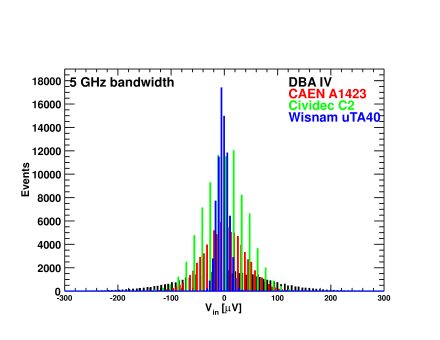
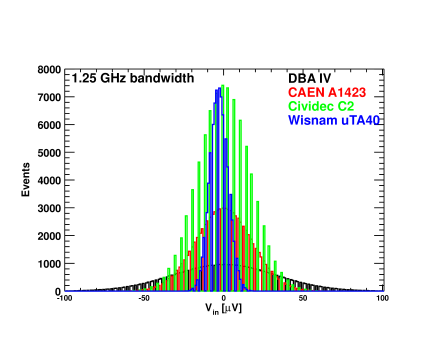
The noise level referred to the input was measured simultaneously with signal acquisition by comparing the voltages in the samples before the signal peak to the baseline voltage. This was done for the full digitizer sampling rate of 5 Gs/s and summing four interleaved channel amplitudes to restrict the sampling rate to 1.25 Gs/s (SIS3305 digitizer analog bandwidth is 2.2 GHz). The resulted distributions are shown in Fig. 3 and their RMS values are indicated in Fig. 4.
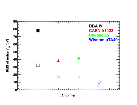
| Amplifier | ||
| [V] | [V] | |
| DBA IVDBA | 78 | 30 (5 dB at 2 GHz) |
| CAEN A1423CAEN | 38 | 26 (5 dB at 1 GHz) |
| Cividec C2Cividec | 41 | 25 |
| Wisnam TA40Wisnam | 10 | NA |
| Cividec C6Cividec | 6 | 1.2 |
We converted these observed noise distributions in projected uncertainty on the collected charge and therefore on deposited energy. To this end we integrated noise output of the amplifier in the same time interval chosen to acquire the signal. The width of the Gaussian distribution of such integrals was extracted. The obtained resolution due to amplifier noise is shown in Fig. 5. In this graph, charge (Cividec Cx) and transimpedance (Cividec C6) amplifier resolutions are also given for comparison. These were obtained with the same technique described so far, but converting noise amplitude into deposited energy equivalent.
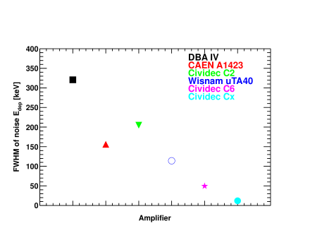
The results shown in Fig. 5 demonstrate the expected superiority of charge and transimpedance amplifiers in terms of energy resolution. Among broadband amplifiers the best resolution of 150 keV was achieved with CAEN A1423.
V Energy resolution
The resolution on the measured charge generated by ionizing particle in CVD diamond is dominated by the amplifier noise. Therefore to compare different amplifiers we measured the charge generated by 5.5 MeV particles produced by 241Am source placed at 6 mm distance. To calibrate the energy scale we assumed that the peak observed in the spectra corresponded to 5.05 MeV as shown in Fig. 6.
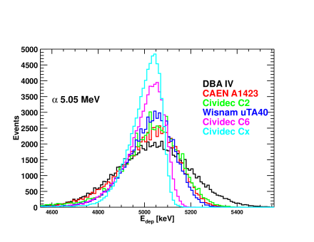
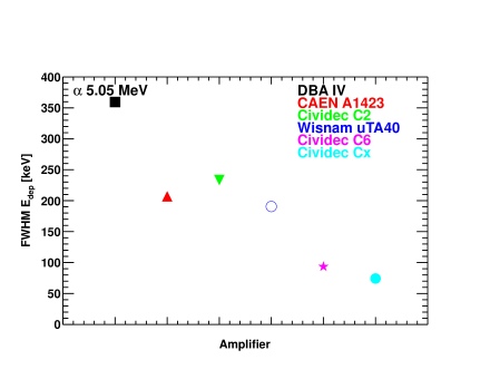
Current amplifiers have poorer resolution, which does not allow to distinguish secondary peaks at lower energy, leading to almost Gaussian peak shapes. Instead both charge and transimpedance amplifiers show more detailed energy distributions. The experimental resolution was measured for each amplifier by a fit of the observed peak by a Gaussian function. For charge and transimpedance amplifiers only the high energy side of the peak was fitted. The measured resolution of all current amplifiers lies around 200 keV FWHM, except for DBA IV amplifier which shows a resolution inferior by a factor two. The experimental resolution of charge and transimpedance amplifiers was found to be larger than the expectation based on their noise. This additional peak broadening is ascribed to fluctuations of energy loss in the 6 mm of air (about 400 keV).
VI Minimal threshold
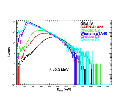
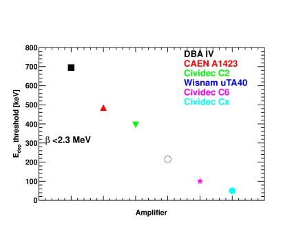
Another important aspect of diamond detector readout is the minimal achievable threshold. This depends on the amplifier noise and gain characteristics. In order to measure the threshold values we used 90Sr source with maximum energy of 2.3 MeV. The digitizer threshold was set to the minimal value that limit noise rate to 100 Hz. The response of the diamond detector, read out by means of different amplifiers, is shown in the left plot of Fig. 7. For different amplifiers the decay spectrum is cut at different energies. The cut-off energy determines the minimal achievable threshold. In the right plot of Fig. 7 the values of the threshold estimated as the energy at which the spectrum reaches half of its maximum.
However, because the physical -spectrum was not flat in energy, at low deposited energies keV these estimates were not always valid. Indeed, the real threshold of the charge amplifier Cividec Cx was about 50 keV, while the transimpedance amplifier Cividec C6 had the real threshold around 100 keV. Instead, the threshold estimate for the fast current amplifier Wisnam TA40 came out correctly to be 200 keV.
VII Pulse shape and timing resolution
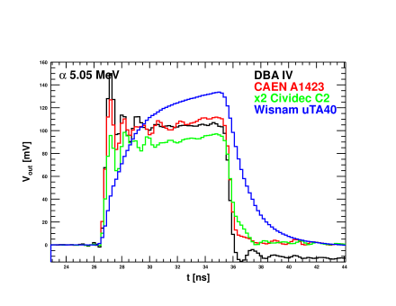
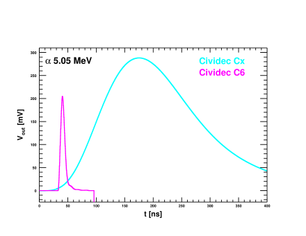
We performed timing and pulse shape measurements by studying coincidences between signals from the two opposite electrodes of the diamond detector, which were acquired by the SIS3305 digitizer in 5 Gs/s mode. Waveforms of both signals were stored on disk. The timing resolution was determined off-line. First of all the signal shapes were acquired for each amplifier as shown in Fig. 8 in one-side readout mode. The obtained pulse shapes were parametrized with opportune RC and semi-Gaussian functions. The pulse shapes of the three broadband amplifiers: DBA IV, CAEN A1423 and Cividec C2 are very similar and reproduce the corresponding input signals. In these pulse shapes fast oscillations were observed at the beginning of the pulse. The period of these oscillations is about 1 ns, which is similar to twice the length of closed circuit from the amplifier input connector pole through the diamond to the short at the opposite diamond electrode (about 16 cm). Therefore, these oscillations can be explained by the reflections of the signal due to incomplete impedance matching. The Wisnam TA40 amplifier showed reduced bandwidth of about 500 MHz, compared to 1.5-2 GHz of DBA IV, CAEN A1423 and Cividec C2. The bandwidth was deduced from its pulse shape, altered by the RC-integration and having much larger rise-time. The transimpedance amplifier Cividec C6 gives relatively fast, 15 ns long, signals with semi-Gaussian shaping rising in about 5 ns. The charge amplifier Cividec Cx generates 350 ns long signals with semi-Gaussian shaping and rise-time of about 130 ns. The latter signal was not suitable for timing applications, but exhibited best energy resolution. It was used only as a reference for diamond energy response.
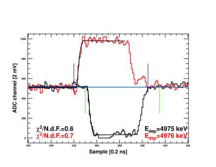
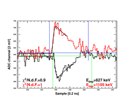
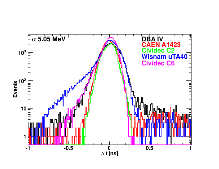
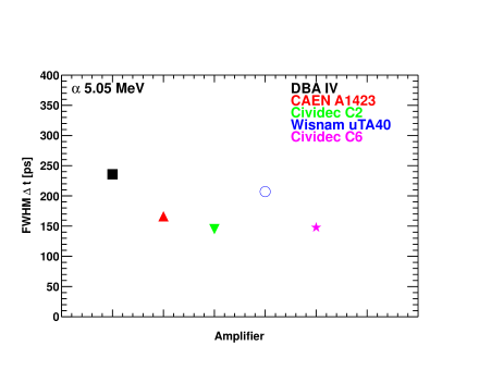
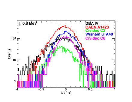
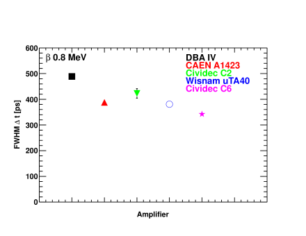
For each measured coincidence event both waveforms, shown for example in Fig. 9, were fitted with selected functions to determine two start times. The difference between these two start times was taken to be the coincidence time difference. For large signals of 5.05 MeV s shown in Fig. 10 the coincidence time difference is nearly Gaussian, except for Wisnam TA40 amplifier, which exhibits some tail at the l.h.s. of the main peak. This tail is due to inaccurate description of the pulse shape. The best overall timing resolution at 5.05 MeV was about 150 ps FWHM, achieved with Cividec C2 and Cividec C6 amplifiers. Wisnam TA40 and DBA IV amplifiers showed ps resolution at 5.05 MeV.
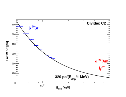
For smaller signals of 800 keV left by s from 90Sr source the timing resolution was considerably worse. The energy dependence of the measured timing resolution can be compared to the naive expectation:
| (2) |
which, assuming linear signal rise, can be rewritten as:
| (3) |
where signal-to-noise ratio can be calculated as the input signal peak voltage to the input referred noise RMS :
| (4) |
Assuming triangular pulse shape, as in case of signals produced by particles, the peak voltage can be related to the total energy deposited in the detector as following:
| (5) |
where is the amplifier input impedance. The signal width, in turn, can be expressed as following:
| (6) |
where carrier drift velocity for a given bias voltage can be measured as the length of signals:
| (7) |
In our case at V/m and m we measured ns. This corresponds to the carrier mean velocity:
| (8) |
Combining the above equations, the input signal peak voltage can be rewritten as following:
| (9) |
Finally substituting this into Eq. 3 we obtain the approximate expression for timing resolution:
| (10) |
In the case of Cividec C2 amplifier and therefore at MeV we obtain:
| (11) |
The above expression describes well the measured timing resolution for ps. This value is in agreement with observed rise time in Fig. 9, and consists of detector capacitance ps, Cividec C2 amplifier risetime of 170 ps and a smaller contribution due to secondary amplifier and cables.
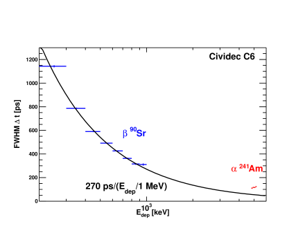
In the case of Cividec C6 amplifier the resolution can be estimated from its sensitivity of 3 mV/fC and its linear gain :
| (12) |
This combined with the amplifier noise value gives the timing resolution:
| (13) |
At MeV and Cividec C6 rise time ns this estimate would imply timing resolution of ps, which is factor of 6 larger than the measured ps. Our noise RMS was measured with 2 GHz bandwidth for a 100 MHz amplifier, using instead the declared noise value allowed to describe the measured timing resolution.
| Amplifier | FWHM at 1 MeV | for MIPs in 500 m |
| [ps] | [ps] | |
| DBA IV | 377 | 516* |
| CAEN A1423 | 240 | 329* |
| Cividec C2 | 226 | 310* |
| Wisnam TA40 | 181 | 248 |
| Cividec C6 | 191 | 262 |
VIII Remote Detector
In many experiments the amplifier cannot be installed close to the detector. Insertion of a cable between detector and the amplifier introduces noise and signal distortions, in particular when the impedance of the cable and amplifier is not well matched. This is particularly important for charge and transimpedance amplifiers. Standard broadband amplifiers featuring 50 input impedance are almost insensitive to the insertion of the input cable. In our application the presence of a 1.5 m long cable is mandatory. Hence we tested transimpedance and charge amplifiers Cividec C6 and Cividec Cx with four different cables: 150 cm of 50 /87 pF/m SF105 (indicated as RG58), 150 cm of 75 /67 pF/m RG59, 166 cm of 93 /44 pF/m RG62, 616 cm of 185 /22.3 pF/m RG114.
The comparison of signals produced by Cividec C6 and Cividec Cx amplifiers connected to the detector via different cables is shown in Fig. 13.
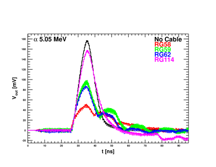
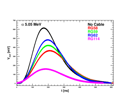
Using the Cividec C6 amplifier, the insertion of a cable leads to strong signal reflections, reducing for higher impedance cables and almost absent for 185 RG114 cable111However, for another amplifier of the same model we observed reflections also with RG114 cable.. From this we deduce that the amplifier input impedance is about 200 . Using Cividec Cx amplifier cable insertion leads to signal suppression proportional to the overall capacitance of the cable. Indeed, the RG62 cable with 44 pF/m capacitance shows smallest suppression, while RG114 with 22.3 pF/m capacitance exhibits larger suppression because its 4 times larger length. This can be better quantified by measuring peak amplitude of the output signals as shown in Fig. 14.
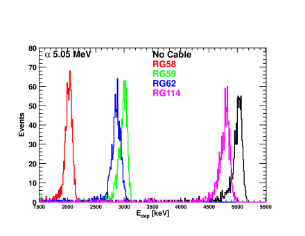
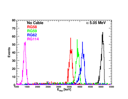
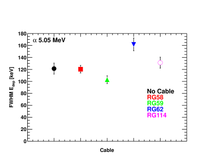
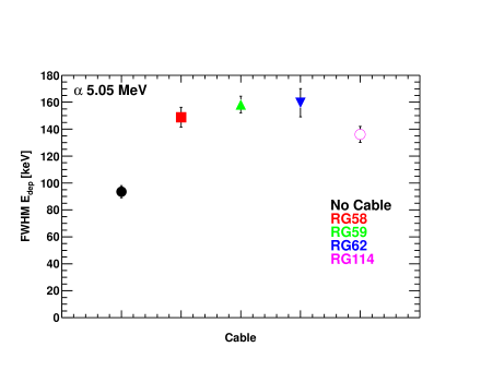
The energy resolution variations due to insertion of different cables are different for two amplifiers as shown in Fig. 15. Cividec C6 amplifier energy resolution changes by about 10% with RG114 and RG62 cables, while no effect is observed for other cables. For Cividec Cx amplifier insertion of any cable leads to 30-40% resolution loss.
IX Summary
A number of modern commercial amplifiers for diamond detectors were characterized for typical nuclear and particle physics applications. These include four broadband amplifiers one transimpedance amplifier and one charge amplifier. We compared their energy and timing resolutions in order to select the best candidate for measuring 200 keV deposited energy signals. Among these amplifiers only Cividec C6 and Cividec Cx amplifiers are able to reach energy thresholds as low as 100 keV. However, the latter one is charge amplifier featuring very long signals, not suitable for for timing application. The obtained timing resolution at 200 keV of the only amplifier which met our requirements, the Cividec C6, was found to be 1.2 ns (resolution of two Cividec C6 amplifiers in coincidence), which was factor of 6 larger than our target resolution of 200 ps. This resolution could be further reduced by a factor by differential readout of the detector, but would remain factor of 4 above the requirement.
The Wisnam TA40 amplifier allows to measure 200 keV signals, but the resolution is similar to the one of Cividec C6.
These results call for development of a new amplifier with signal-to-noise ratio improved by a factor of 10 with respect to the tested ones.
References
- (2) E6 Element Six Ltd, http://www.e6cvd.com/cvd
- (4) Struck Innovative Systeme, http://www.struck.de/sis3305.html
- (5) H. Kagan and W. Trischuk, CVD Diamond for Electronic Devices and Sensors, Wiley, p.207 (2009).
- (6) Diamond Detector Ltd, http://www.diamonddetectors.com
- (7) http://www.ge.infn.it/~osipenko/sis3305/sis3305_rev2c.zip
- (8) P. Moritz, E. Berdermann, K. Blasche, H. Stelzer and F. Zeytouni, Diamond detectors for beam diagnostics in heavy ion accelerators, Frascati, 153-155 (1997).
- (9) CAEN S.p.A., http://www.caentechnologies.com
- (10) CIVIDEC Instrumentation GmbH, http://www.cividec.at
- (11) WiSNAM S.r.l., http://www.wisnam.com