Controlling the Spontaneous Emission Rate of Monolayer MoS2 in a Photonic Crystal Nanocavity
Abstract
We report on controlling the spontaneous emission (SE) rate of a molybdenum disulfide (MoS2) monolayer coupled with a planar photonic crystal (PPC) nanocavity. Spatially resolved photoluminescence (PL) mapping shows strong variations of emission when the MoS2 monolayer is on the PPC cavity, on the PPC lattice, on the air gap, and on the unpatterned gallium phosphide substrate. Polarization dependences of the cavity-coupled MoS2 emission show a more than 5 times stronger extracted PL intensity than the un-coupled emission, which indicates an underlying cavity mode Purcell enhancement of MoS2 SE rate exceeding a factor of 70.
The recent finding that a single atomic layer of transition metal dichalcogenides (TMDs) can exhibit a large, direct bandgap Wang2012o ; Mak2010b ; Han2011a ; Kadantsev2012 opens the possibility of a new range of atomically thin materials for electronic and electro-optic devices. Monolayer molybdenum disulfide (MoS2) has been used to fabricate field-effect transistors (FETs) with a carrier-mobility of 200 cm2V-1s-1 and On/Off ratios exceeding 108 at room temperature, comparable to those obtained in graphene nanoribbon-based FETs Radisavljevic2011 . Optical studies have shown that monolayer MoS2 exhibits a photoluminescence (PL) quantum yield that is enhanced by a factor more than 104 compared with the bulk crystal Mak2010b ; Splendiani2010 . However, the PL efficiency of monolayer MoS2 is still very low at because the nonradiative recombination rate far exceeds the spontaneous emission (SE) rate Mak2010b . For MoS2 monolayers on SiO2 substrate, values of ps and ns were estimated at room temperature Korn2012 ; Mak2010b . Here, we show that the SE efficiency of an MoS2 monolayer can be greatly enhanced by exploiting the strong Purcell effect in photonic crystal nanocavities to shorten the radiative recombination time. After depositing an MoS2 monolayer onto a planar photonic crystal (PPC) nanocavity, we observe an enhancement of the external extracted PL intensity by a factor of 5.4 above the background. This strong enhancement exists even though the collection is from the sub-wavelength cavity mode and the surrounding focal spot region. Taking into account this spatial averaging, we deduce that the SE rate enhancement into the cavity mode corresponds to nearly a factor of 70, in close agreement with theory. These results indicate that by exploiting the strong Purcell effect in optical cavities with wavelength-scale mode volume and high quality () factor, it is possible to achieve roughly two orders of magnitude improvement in the MoS2 PL efficiency. This gain opens the door to efficient light emissions from, and strong light-matter interactions with, materials of atomic thickness.

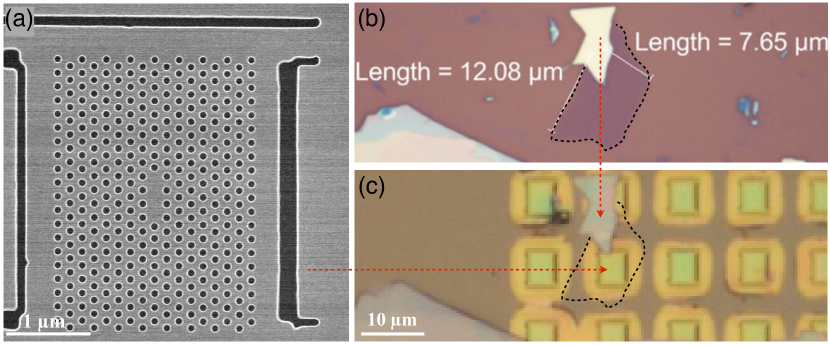
The experiment employs PPC nanocavities fabricated in a 138 nm thick gallium phosphide (GaP) membrane using electron-beam lithography, dry etching, and wet chemical undercutting of an AlGaP sacrificial layer Gan2012b . The cavity design is a linear three-missing hole (L3) defect Noda2003Nature with a lattice spacing nm and an air-hole radius , yielding resonant modes in the wavelength range of 600 nm-700 nm to overlap the PL spectrum of the monolayer MoS2. Figure 1(a) shows a scanning electron microscope (SEM) image of the PPC nanocavity before the deposition of MoS2. Trenches around the PPC lattice aid in the removal of the sacrificial layer in a hydrofluoric acid bath. The monolayer MoS2 is prepared by mechanical exfoliation onto a polymeric sacrificial substrate, as shown in the optical microscope image in Fig. 1(b). Due to the optical interference, MoS2 monolayer is clearly visible in the purple region indicated by the dashed black line, which is also confirmed by a micro-Raman spectroscopy Mos2010 . The MoS2 sheet is then transferred onto PPC nanocavities through a precision transfer technique with the help of the polymeric sacrificial substrate, which is removed from the final device by high-temperature annealing 2010.NNano.Hone.graphene . Figure 1(c) shows the finished device. An PPC nanocavity is covered uniformly by the MoS2 monolayer, which is clearly distinguished by correlating the above multi-layer MoS2 flake.

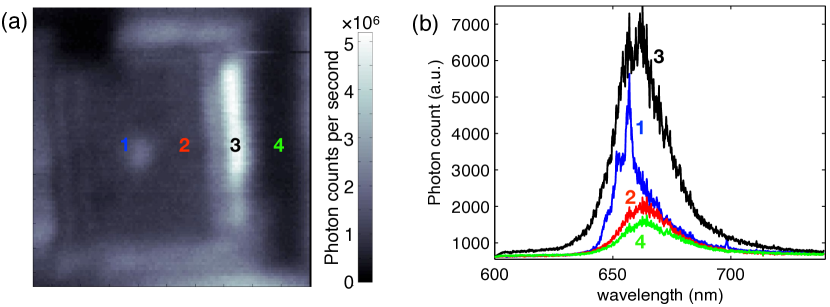
We characterize the device on a micro-PL confocal microscope with a 532 nm continuous-wave excitation laser, focused to a beam diameter of 400 nm and with a power of 50 W. To study the modifications on the MoS2 SE, we spatially scan the device in 50 nm steps on a piezo stage and detect the MoS2 PL using an avalanche photodiode. Figure 2(a) shows the spatially resolved PL. By correlating it with the SEM image shown in Fig. 1(a), we observe four individual emission profiles of MoS2 due to different substrates, as marked in Fig. 2(a). The spectrally resolved PL of the four regions are shown in Fig. 2(b). The result reveals that the PL collected from region 3, where the MoS2 sheet is suspended over a 300 nm wide trench, is significantly brighter than that obtained from region 4 on the bulk GaP membrane. This is expected due to the suppression of the PL quantum yield by the substrate Mak2010b and the total internal reflection of the high-index GaP slab 2005.Science.Noda.SE_control , which sharply reduces the PL collection efficiency. On both regions, the monolayer MoS2 emits the same fluorescence spectrum centered around 660 nm due to the direct electronic bandgap Mak2010b .
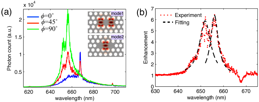
On the PPC, we observe both an enhancement and a suppression of the MoS2 PL emission. In region 2, due to the coupling between the periodic air-holes of the PPC lattice and the MoS2 sheet, the in-plane emission channel is inhibited by the in-plane photonic bandgap, which overlaps with the emission band of the monolayer MoS2. Therefore, the SE should be re-directed into near-vertical -vectors within the PPC light cone 2005.Science.Noda.SE_control . This SE redistribution and the higher collection efficiency from the PPC lattice enhances the collection of emission into the vertical direction via the suppression of emission into in-plane PPC modes. Hence, the collected photon flux from region 2 is brighter than that from the bulk GaP membrane, as confirmed from the PL spectra. However, the PL collected from the L3 defect (region 1) shows even brighter emission than that from region 2. Comparing the spectra acquired from region 1 and region 2, it is clear that this enhancement mainly results from a greatly amplified photon flux of the two peaks at the wavelengths of 655.4 nm and 656.9 nm. The polarization dependences of the two peaks from region 1 are then resolved by rotating a polarizer in the PL collection path of the microscope setup. The obtained spectra are shown in Fig. 3(a), where denotes the angle between the cavity -axis and the polarization direction of the polarizer. These spectra indicate the two peaks at 655.4 nm and 656.9 nm are the resonant modes of the L3 cavity with expected polarization and wavelength dependences matching the three-dimensional finite difference time domain (FDTD) simulations 2007.APL.UK_ppl.mode_structure_L3 ; Schwagmann2012 , which also confirm other resonant modes of the peaks at longer wavelength. Therefore, over the cavity defect region, the simultaneous suppression of SE into in-plane PPC modes together with the cavity mode Purcell enhancement of SE rate results in a dramatic reshaping of the MoS2 SE, as was previously shown for single emitters 2005.PRL.Englund ; Kress2005 ; Kaniber2007 and quantum wells 2005.Science.Noda.SE_control in PPC cavities.
For simplicity, we designate the two resonant modes at 655.4 nm and 656.9 nm as mode 1 and mode 2, respectively. Fitting the peaks to Lorentzian lineshapes, we find that the factors of the two modes are and 320, respectively, which degrade from the initial factors of 880 and 800 of the unloaded cavity due to the spectrally overlap with the absorption resonance of the monolayer MoS2 Mak2010b ; Gan2012 ; Gan2013b . The simulated cavity fields of modes 1 and 2 are shown in the inset of Fig. 3(a), which have mode volumes () of 0.63 and 0.33, where is the refractive index of GaP.

To quantitatively anaylse the cavity enhancement of MoS2 SE rate, we model the coupled MoS2-cavity system by considering the MoS2 as a collection of excitonic dipole emitters. The exciton recombination rate is given by a sum over radiative and non-radiative recombination rates, . In our experiments, the PL intensities at the resonant wavelengths show linear dependence on the excitation power, verifying that the SE processes are far below the saturation rate of the MoS2 sheet. Therefore, the emission power is proportional to where is the excitation power and is the absorbance of monolayer MoS2 at the excitation wavelength. Because in MoS2 and the finite collection angle of optics, we can approximate for all of our experiments that , where is the collection efficiency of the PL emission. Here, we consider the excitons as an ensemble of emitters in the MoS2 on a bulk substrate have a natural SE rate with a transition rate corresponding to the spectral range from to . The modified SE distribution when the MoS2 sheet is on the PPC nanocavity is given by
| (1) |
Here, denotes the cavity’s Lorentzian spectrum with as the resonant wavelength, and denotes the spatial and angular overlaps between the emitter dipole and the cavity field . The factor is the maximum SE enhancement (Purcell) factor of the cavity mode when the emitter dipole is on resonance with the cavity and spatially aligned with the cavity field. The term accounts for the suppression of the SE rate by the PPC lattice and modes other than the cavity mode 2005.PRL.Englund ; 2005.Science.Noda.SE_control .
The total cavity-coupled MoS2 emission spectrum with different polarizations can be fitted to a model that considers both the SE rate modifications and the collection efficiencies of the cavity mode and averaged PPC leaky modes. We calculate by integrating the SE rate given in Eq. (1) over the spatial and in-plane orientation densities of the emitter dipoles
| (2) |
Here, and are the coupling efficiencies into the objective lens of the PL emissions coupled with the cavity mode and averaged PPC leaky modes. Due to the primarily linear polarization dependence of the cavity modes 1 and 2, the PL spectra shown in Fig. 3(a) with polarizations as and indicate the off- and on-resonance emissions. We calculate the spectrally resolved cavity-enhancement of the collected emission from the two spectra, as shown in Fig. 3(b), which is governed by
| (3) |
By integrating the far-field radiations of a dipole spectrally on- or slightly off-resonance with the cavity mode over the numerical aperture (NA=0.95) of the objective lens, which locates on the cavity defect, we obtain the coupling efficiencies ratios for modes 1 and 2 are 87% and 73%, respectively Gan2013c . The integral over the angle of the dipole with respective to the cavity field equals to due to the random orientations of dipoles on the two-dimensional MoS2 sheet. The spatial density of the dipoles corresponds to the excitation of a uniform MoS2 area by a Gaussian beam with a full width at half maximum of about 400 nm in the plane. Over this excitation area, the spatial integral of are 0.169 and 0.079 for modes 1 and 2, respectively, as calculated from their simulated cavity fields. With the calculated and the factors derived from the experimental spectra, we calculate the maximum Purcell factor for modes 1 and 2 are about 26.5 and 73.8. The suppression factor is estimated by simulating the emission power ratio of a dipole on the L3 cavity defect and on the bulk membrane 2005.PRL.Englund . The emission frequency of the dipole is chosen in the photonic bandgap of PPC but off-resoance with the cavity mode. The obtained is approximately 0.4, which is close to the values found in similar PPC structures 2005.PRL.Englund ; 2005.Science.Noda.SE_control ; 2005.APL.Fushman.PbS . Combining the above calculations and the Lorentizan functions of modes 1 and 2, the theoretical model described in Eq. (3) shows a good fit to the experimentally obtained enhancement spectrum, as shown in Fig. 3(b).
In conclusion, we have shown that by coupling monolayer MoS2 to an PPC nanocavity, it is possible to dramatically enhance its internal quantum efficiency for transitions on resonant with the cavity. The experimental results and theoretical calculations reveal that the maximum enhancement of the MoS2 SE rate by the cavity modes can be higher than 70, with a suppression factor of about 0.4 due to the PPC lattice. In this work, the strong Purcell enhancement was limited to the sub-wavelength size of the cavity; however, a high Purcell enhancement across a larger area could be realized using slow light near the bandedge of photonic crystals or coupled cavity arrays Altug2005 . The cavity-enhanced light-matter coupling in monolayer MoS2 indicated by the strong Purcell effect expands the scope of solid state cavity quantum electrodynamics to atomically thin materials with large bandgaps, which has implications for a range of optical devices, including efficient photodetectors Lopez-Sanchez2013 and electroluminescent systems, cavity-enhanced nonlinearities Kumar2013 and potentially even lasers employing atomically thin gain media.
Acknowledgment: The authors thank Kangmook Lim and Edo Waks for the dry etching of PPC cavities. Financial support was provided by the Air Force Office of Scientific Research PECASE, supervised by Dr. Gernot Pom- renke, the DARPA Information in a Photon program, through Grant No. W911NF-10-1-0416. Device fabrication was partly carried out at the Center for Functional Nanoma- terials, Brookhaven National Laboratory, which is supported by the U.S. Department of Energy, Office of Basic Energy Sciences, under Contract No. DE-AC02-98CH10886. R.S. was supported in part by the Center for Excitonics, an Energy Frontier Research Center funded by the U.S. Department of Energy, Office of Science, Office of Basic Energy Sciences under Award Number DE-SC0001088. X.G. was partially supported by the 973 program (2012CB921900) and NSFC (61377035).
References
- (1) Q. H. Wang, K. Kalantar-Zadeh, A. Kis, J. N. Coleman, and M. S. Strano, Nature Nanotech. 7, 699 (2012).
- (2) K. F. Mak, C. Lee, J. Hone, J. Shan, and T. F. Heinz, Phys. Rev. Lett. 105, 136805 (2010).
- (3) S. W. Han, H. Kwon, S. K. Kim, S. Ryu, W. S. Yun, D. H. Kim, J. H. Hwang, J. S. Kang, J. Baik, H. J. Shin, and S. C. Hong, Phys. Rev. B 84, 045409 (2011).
- (4) E. S. Kadantsev and P. Hawrylak, Solid State Commun. 152, 909 (2012).
- (5) B. Radisavljevic, A. Radenovic, J. Brivio, V. Giacometti, and A. Kis, Nature Nanotech. 6, 147 (2011).
- (6) A. Splendiani, L. Sun, Y. Zhang, T. Li, J. Kim, C. Chim, G. Galli, and F. Wang, Nano Lett. 10, 1271 (2010).
- (7) T. Korn, S. Heydrich, M. Hirmer, J. Schmutzler, C. Schuller, and C. Schu, Appl. Phys. Lett. 99, 102109 (2011).
- (8) X. Gan, N. Pervez, I. Kymissis, F. Hatami, and D. Englund, Appl. Phys. Lett. 100, 231104 (2012).
- (9) Y. Akahane, T. Asano, B. S. Song, and S. Noda, Nature 425, 944 (2003).
- (10) C. Lee, H. Yan, L. Brus, T. F. Heinz, J. Hone, and S. Ryu, ACS Nano 4, 2695 (2010).
- (11) C. R. Dean, A. F. Young, I. Meric, C. Lee, L. Wang, S. Sorgenfrei, K. Watanabe, T. Taniguchi, P. Kim, K. L. Shepard, and J. Hone, Nature Nanotech. 5, 722 (2010).
- (12) M. Fujita, S. Takahashi, Y. Tanaka, T. Asano, and S. Noda, Science 308, 1296 (2005).
- (13) A. R. A. Chalcraft, S. Lam, D. OBrien, T. F. Krauss, M. Sahin, D. Szymanski, D. Sanvitto, R. Oulton, M. S. Skolnick, A. M. Fox, D. M. Whittaker, H. Y. Liu, and M. Hopkinson, Appl. Phys. Lett. 90, 241117 (2007).
- (14) A. Schwagmann, S. Kalliakos, D. J. P. Ellis, I. Farrer, J. P. Griffiths, G. C. Jones, D. Ritchie, and A. J. Shields, Opt. Express 20, 28614 (2012).
- (15) D. Englund, D. Fattal, E. Waks, G. Solomon, B. Zhang, T. Nakaoka, Y. Arakawa, Y. Yamamoto, and J. Vuckovic, Phys. Rev. Lett. 95, 13904 (2005).
- (16) A. Kress, F. Hofbauer, N. Reinelt, M. Kaniber, H. Krenner, R. Meyer, G. B?ohm, and J. Finley, Phys. Rev. B 71, 241304 (2005).
- (17) M. Kaniber, A. Kress, A. Laucht, M. Bichler, R. Meyer, M. C. Amann, and J. J. Finley, Appl. Phys. Lett. 91, 061106 (2007).
- (18) X. Gan, K. F. Mak, Y. Gao, Y. You, F. Hatami, J. Hone, T. F. Heinz, and D. Englund, Nano Lett. 12, 5626 (2012).
- (19) X. Gan, R. Shiue, Y. Gao, K. F. Mak, X. Yao, L. Li, A. Szep, D. Walker, J. Hone, T. F. Heinz, and D. Englund, Nano Lett. 13, 691 (2013).
- (20) X. Gan, H. Clevenson, C. Tsai, L. Li, and D. Englund, Sci. Rep. 3, 2145 (2013).
- (21) I. Fushman, D. Englund, and J. Vuckovic, Appl. Phys. Lett. 87, 241102 (2005).
- (22) H. Altug and J. Vuckovic, Appl. Phys. Lett. 86, 111102 (2005).
- (23) O. Lopez-Sanchez, D. Lembke, M. Kayci, A. Radenovic, and A. Kis, Nature Nanotech. 8, 497 (2013).
- (24) N. Kumar, S. Najmaei, Q. Cui, F. Ceballos, P. M. Ajayan, J. Lou, and H. Zhao, Phys. Rev. B 87, 161403 (2013).