Effects of interface electric field on the magnetoresistance in spin devices
Abstract
An extension of the standard spin diffusion theory is presented by introducing a density-gradient (DG) term that is suitable for describing interface quantum tunneling phenomena. The magnetoresistance (MR) ratio is modified by the DG term through an interface electric field. We have also carried out spin injection and detection measurements using four-terminal Si devices. The local measurement shows that the MR ratio changes depending on the current direction. We show that the change of the MR ratio depending on the current direction comes from the DG term regarding the asymmetry of the two interface electronic structures.
pacs:
72.25.-b,73.43.Qt,85.75.HhSpin injection and detection between silicon and magnetic material via tunneling barriers constitute one of the most important issues in spintronics, and the key factor that determines the performance of spin devices such as spin transistors Tanaka ; Appelbaum ; Dash ; Crowell ; Suzuki ; Li ; Uemura ; Jeon ; Ando ; Jansen ; Saito1 ; InokuchiJAP ; Ishikawa ; Tanamoto ; Zhang ; TanaRT ; Miao . The difference in electronic structure between ferromagnet (FM) and semiconductor (SC) generates the conductance mismatch between the two materials, which has inspired much important research regarding spin transport properties through the interface. With regard to the spin diffusion theory (standard theory) ValetFert ; Schmidt ; Fert2001 ; Jaffres ; Fukuma , which has to a great content succeeded in explaining tunneling phenomena of nonmagnet (NM) sandwiched by two FMs, the challenge is to explain new phenomena that appears in SC: Jansen et al. showed the effect of the depletion layer in the SC interface Jansen0 and pointed out the importance of the consideration of band structure at the interface. Tran et al.Tran ; Jansen1 discussed the relation between the localized states and the enhancement of spin accumulation signal at Co/Al2O3/GaAs interface. Yu et al. Yu derived the drift-diffusion equation without depletion layer and Kameno et al. Kameno experimentally showed the contribution of the spin-drift current in the substrate. Considering the usefulness of the standard spin diffusion theory and the fact that the effects of bulk properties such as spin drift can be taken into account by changing the lifetime or other parameters of the standard theory, it is desirable to extend the present standard theory so that it includes interface effects that are specific to SC.
Here we theoretically extend the standard spin diffusion theory by taking into account the density-gradient (DG) theory that is derived from the quantum diffusion equation Ancona1990 . The DG theory can describe the interface phenomena such as quantum tunneling through SiO2 sandwiched by an electrode and Si substrate Ancona2 ; Ancona3 . This DG term appears when the electron density changes at the interface as a result of the band bending. We apply this DG term which has been studied in the conventional silicon transistors to the two-spin-current model, and we provide an analytic formula of the magnetoresistance (MR) ratio for FM/SC/FM structure. We show that the DG term increases or decreases the MR ratio depending on the current direction through FM/SC/FM structure when there is an electronic structure between the source interface and the drain interface. The direct way to realize the asymmetric electronic states at the two interfaces is to make the areas of the two electrodes different. The different areas of the electrodes generate different depletion region depending on current direction. We have carried out both local and nonlocal measurements for four-terminal silicon devices that have asymmetric electrodes. We show that experimentally obtained MR ratios differ depending on the current direction (from source to drain or from drain to source). The standard theory cannot explain this directionality of MR ratio, because the solution of the diffusion equation in the SC is symmetric between the source and the drain tanaJJAP . The different electronic interfaces break this symmetric state in which the MR ratio has a maximum at the symmetric point.
Formulation.— We take into account the DG term in the spin current to describe the quantum tunneling at the FM/SC interface through a tunneling barrier. The generalized chemical potential is described by
| (1) |
where is the conventional chemical potential (). express a density of electron Ancona1990 ; Ancona2 ; Ancona3 . The second term express the DG term and is a coefficient of this term. The parameter changes depending on the physical environment. Although Ancona et al. use for high-temperature region, and for low-temperature region, we take as a fitting parameter when we apply our theory to experiments. The generalized spin current is given by Ohm’s law given by , where is a spin-dependent conductivity.
We assume that the same macroscopic diffusion equations as those of the standard theories ValetFert ; Fert2001 ; Schmidt hold: and with as an average spin diffusion length. Combining with the current conservation relation given by (const), we have solutions for the differential equations in ferromagnetic region:
| (2) | |||||
| (3) |
with , and ( is a center of -ferromagnet), for both ferromagnetic electrodes . is the resistivity of the FM. We obtained a similar formulation of the chemical potential and the current in the SC region. and are unknown coefficients to be determined by the boundary conditions. with is the DG term (the second term in Eq. (1)), and is its derivative given by .
The same boundary conditions are applied to chemical potential and current at in the standard theories ValetFert ; Fert2001 are applied: and . We also have a current conservation condition other than the interface regions such as where and are areas of -FM and the SC. We define , , and , where is the resistivity of the SC region. The relations of the spin accumulation and the DG term can be derived from Eqs.(2) and (3), and related equations given by
| (4) | |||
| (5) |
Similar equations are obtained at the right interface depending on the parallel (P) and the antiparallel (AP) states. Here include the DG terms given by
Eqs. (4) and (5) indicate that the spin accumulation is determined by the modified current when the DG term exists. Next, we show that the DG term is related with the interface electric field.
Interface electric field.— Strictly speaking, the DG terms are numerically determined by solving the Poisson equations and the Schrödinger equation. However, because many approximations are required to obtain interface electronic structure even without spin accumulation Stern , we would like to take the following simple approximation. From the Schrödinger equation , and the relation , the DG term can be approximately evaluated by
| (6) |
Then we obtain with for the FM region and with for the SC region at the interface of . From the current conservation condition, we have new boundary conditions given by
| (7) |
where is the boundary position. From this condition, we have . Thus, is determined by of the FM regions. Then we obtain . Note that, in the present framework, the thickness of the tunneling barrier between FM/SC is neglected and the connection between the FC and the SC is described at the boundary point ( ). Therefore, we consider that Eq.(6) can include the main effect of the tunneling phenomena.
Magnetoresistance.— Total resistance through the FM/SC/FM structure is obtained by summation of each resistance of the FM and SC elements. The resistance difference is given by
| (8) | |||||
where , , , , and
with being the degree of the asymmetry. The MR ratio is obtained from divided by the total resistance of the parallel magnetic alignment. In the impedance matching region Fert2001 , we have
| (9) |
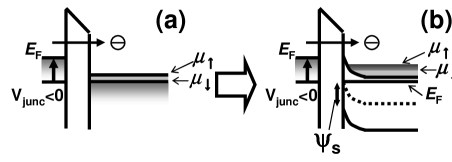
is the MR ratio without the interface effect Fert2001 . We can see that the interface effect modifies the MR ratio by the modified current weighted by area. When , , therefore the asymmetric area is important for increasing the MR ratio. For the symmetric point , and the MR ratio coincides with the conventional formula. When the electrons flow from the left electrode to the right electrode, and (Fig.1), and when the electrons flow from the right electrode to the left, and . Thus, by setting the different interface electric fields depending on the current direction, we can obtain a different MR ratio. These are the main theoretical results of this paper.
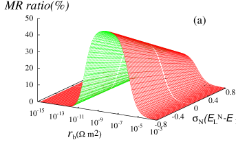
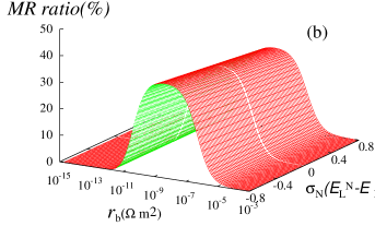
Let us confirm these analyses by numerical calculations assuming . Figure 2 shows the numerical results of the MR ratio as a function of the asymmetry for (a) and (b) . When the asymmetry of the area is large ((a)), the effect of the asymmetric local field becomes large. Moreover, in the region of , which corresponds to , MR ratio increases. This can be understood as follows: the larger depletion region generates larger electric field that accelerates electrons resulting in the larger MR ratio.
In Ref. tanaJJAP , we theoretically showed the MR ratio has its maximum at the symmetric structure () in the range of the standard theory. When there is no interface electric field, , then Eq.(9) becomes . Thus, the MR ratio has its maximum when . This means that a new degree of freedom, , local electric field, enables the change of the MR ratio.
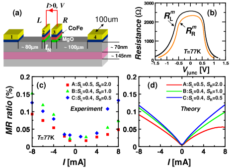
Experiments.— In order to realize the asymmetric electric field, areas of two FM electrodes should be different. We fabricated four-terminal devices for Hanle-effect measurements, as shown in Fig. 3(a) for three types of different area configurations: [A] , and nm, [B] , and nm, [C] , and nm. The CoFe/MgO(1nm) is patterned on a phosphorus-doped () (100) textured Si of an insulator (SOI) substrate, where ohmic pads consisting of Au/Ti were formed for all the contacts. The structures will be discussed in detail elsewhere Ishikawa2 . Figure 3(b) shows the resistance-voltage (-) characteristics of the left () and the right () tunneling junctions for the device , which are derived from current-voltage (-) measurements. Here, positive bias corresponds to a case where electrons flow from SC to FM. The measured resistance of the junction, , is always larger than that of the right electrode, , because . In addition, it is found that the resistances of are larger than those of . This means that the depletion layer in SC appears when electrons flow from FM to SC while there is no depletion layer in SC when electrons from SC to FM. Hence, the resistance can be regarded as the intrinsic junction resistances ( and ).
Figure 3(c) shows MR ratio as a function of current through the terminals 2 and 3 (local measurement, see also Fig. 3(a) for the current direction). In the standard theory, MR ratio is described as a function of current, and therefore, hereafter we analyze our experiments as a function of current through terminal 2 and 3. We can see that (i) the MR ratio changes in proportion to the current (or bias), and (ii) the MR ratio differs depending on or . Remember that MR ratio of the single junction has a peak at the zero bias (zero current) Jansen0 ; Luders . In addition, the MR ratio derived by the standard theoryFert2001 does not include the direction of current. These phenomena can be understood by considering the local electric fields as follows: () corresponds to a case when () for -junction and () for -junction. Because of the area difference and Fig. 3(b), the depletion region of the right junction for is smaller than that of the left junction for , and is realized. Then, MR ratio for is larger than that for . These results show a new picture of the spin transport in the local measurement. The result that this asymmetry is clearest for device and least for supports the view that the asymmetry comes from the strength of the interface electric field.
Next let us quantitatively compare the theory with the experiment. In the metal-insulator-semiconductor(MIS) interface, we have , where , , ,, and are the flat-band shift, the voltage fluctuation by trap states, the electric field applied to the junction, the thickness of the junction and the surface potential, respectively Sze . is estimated by donor density and temperature K with nm at low-bias region ( 2 V). In this region, the number of holes is neglected and electrons at are in a depletion region with . The coefficient is used as a fitting parameter, because the interface electric field is not uniform in view of the geometry and the interface roughness. Concretely we take assuming 5 nm depletion layer with the average resistance and current estimated from the experiment. When the parameters such as Fig. 3(b) are included, the numerical MR ratio is given in Fig. 3(d). As can be seen, we can realize the overall tendency of the experiment. If we apply the experimental parameters to the standard theory, the MR ratio for is larger than that for . From Fig.3, the difference between the left and the right junction resistances is smaller for than that for . By considering that the symmetric structure produces larger MR in the standard theory, the MR ratio of is larger than that of in the standard theory.
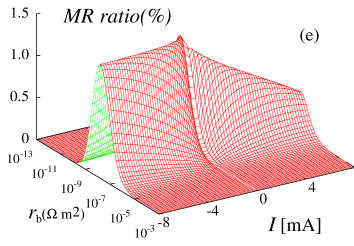
Figure 3(e) shows the MR ratio of devices as functions for the interface resistance and the current. The difference from Fig. 2 is that we use the experimental - characteristics (Fig. 3) in which and increases when decreases. This is the reason why MR ratio increases as a function current in Fig. 3 (c) ( of our experiments is larger than the conductance matching peak). The MR ratio of the device is larger than that of the device because the distance between two electrodes of the former is smaller than that of the latter. From Fig. 3(e), it is also predicted that the MR ratio decreases as current increases when is smaller than its impedance matching point(backside of Fig. 3(e)).
Discussion.— Kameno et al. showed that the spin drift makes lifetime depend on applied voltage Yu ; Kameno . We conducted a lifetime measurement in a three-terminal setup and found there was no bias-voltage dependence on the lifetime Ishikawa2 . This is considered to be because the FM areas of our devices are more than two times larger than those in Ref. Kameno . Note that even a small change in the MR ratio requires a larger change of the lifetime because . Thus, the spin drift seems not to be the main cause of the change of the MR ratio in our devices. Thus, the change of the MR ratio mainly comes from the asymmetric electronic structure, including the area difference indicated by Eq.(8).
The effect of trap sites has not yet been explicitly included in the proposed theory. Change of lifetime as shown in Ref. Tran might be the direct way to include the effect of trap sites. The trap sites could also affect the MR ratio through the change of from which is estimated. Here, we treat the coefficient as a fitting parameter, because the determination of the coefficient requires more detailed experiments. The estimation of the effect of traps is a subject for future work.
In summary, we introduced the density-gradient effect into the standard spin diffusion theory, and conducted both the local and nonlocal measurements on n-type Si devices. We showed that the increase/decrease of the MR ratio comes from the asymmetry of the two interface electronic structures and explained why the experimentally obtained MR ratio depends on the current direction.
We thank A. Nishiyama, K. Muraoka, S. Fujita and K. Tatsumura for fruitful discussions.
References
- (1) S. Sugahara and M. Tanka, Appl. Phys. Lett. 84, 2307 (2004).
- (2) I. Appelbaum, B. Huang, and D. J. Monsma, Nature (London) 447, 295 (2007).
- (3) S. P. Dash, S. Sharma, R. S. Patel, M. P. Jong, and R. Jansen, Nature (London) 462, 491 (2009).
- (4) X. Lou, C. Adelmann,, M. Furis, S. A. Crooker, C. J. Palmstrom, and P. A. Crowell, Phys. Rev. Lett. 96, 176603 (2006).
- (5) T. Suzuki, T. Sasaki, T. Oikawa, M. Shiraishi, Y. Suzuki, and K. Noguchi, Appl. Phys. Express 4, 023003 (2011).
- (6) C. H. Li, O. M. J. van’t Erve, and B.T. Jonker, Nat. Commun. 2, 245 (2011).
- (7) T. Uemura, T. Akiho, M. Harada, K.-i. Matsuda, and M. Yamamoto, Appl. Phys. Lett. 99, 082108 (2011).
- (8) K. R. Jeon, B. C. Min, I. J. Shin, C. Y. Park, H. S. Lee, Y. H. Jo, and S. C. Shin, Appl. Phys. Lett. 98, 262102 (2011).
- (9) Y. Ando, K. Kasahara, S. Yamada, Y. Maeda, K. Masaki, Y. Hoshi, K. Sawano, M. Miyao, and K. Hamaya, Phys. Rev. B 85, 035320 (2012).
- (10) R. Jansen, Nat. Mater. 11, 400 (2012).
- (11) Y. Saito, M. Ishikawa, T. Inokuchi, H. Sugiyama, T. Tanamoto, K. Hamaya, N. Tezuka, IEEE Tran. Magn. 48, 2739 (2012).
- (12) T. Inokuchi, M. Ishikawa, H. Sugiyama, Y. Saito, N. Tezuka, J. Appl. Phys. 111, 07C316 (2012).
- (13) M. Ishikawa, H. Sugiyama, T. Inokuchi, K. Hamaya and Y. Saito, Appl. Phys. Lett. 100, 252404 (2012).
- (14) T. Tanamoto, H. Sugiyama, T. Inokuchi, T. Marukame, M. Ishikawa, K. Ikegami, and Y. Saito, J. Appl. Phys. 109, 07C312 (2011).
- (15) X. Zhang, B. Li, G. Sun, and F. Pu, Phys. Rev. B 56, 5484 (1997).
- (16) T. Tanamoto and S. Fujita, Phys. Rev. B 59, 4985 (1999).
- (17) G.X. Miao, M. Muller, and J. S. Moodera, Phys. Rev. Lett. 102, 076601 (2009).
- (18) T. Valet and A. Fert, Phys. Rev. B 48, 7099 (1993).
- (19) G. Schmidt, D. Ferrand, L.W. Molenkamp, A.T. Filip, and B.J. van Wees, Phys. Rev. B 62, R4790 (2000).
- (20) A. Fert and H. Jaffrés, Phys. Rev. B 64, 184420 (2001).
- (21) H. Jaffrés, J. -M. George, and A. Fert, Phys. Rev. B 82, 140408(R) (2010).
- (22) Y. Fukuma, L. Wang, H. Idzuchi, and Y. Otani, Appl. Phys. Lett. 97, 012507 (2010).
- (23) R. Jansen and B. C. Min, Phys. Rev. Lett. 99, 246604 (2007).
- (24) M. Tran, H. Jaffrés, C. Deranlot, J.-M. George, A. Fert, A. Miard, and A. Lemaitre, Phys. Rev. Lett. 102, 036601 (2009).
- (25) R. Jansen, A. M. Deac, H. Saito, and S. Yuasa, Phys. Rev. B 85, 134420 (2012).
- (26) Z. G. Yu and M. E. Flatte, Phys. Rev. B 66, 201202(R) (2002).
- (27) M. Kameno, Y. Ando, E. Shikoh, T. Shinjo, T. Sasaki, T. Oikawa, Y. Suzuki, T. Suzuki, and M. Shiraishi, Appl. Phys. Lett. 101, 122413 (2012).
- (28) M.G. Ancona, Phys. Rev. B 42, 1222 (1990).
- (29) M.G. Ancona, Phys. Rev. B 46, 4874 (1992).
- (30) M.G. Ancona Z. Yu, R.W. Dutton, P.J.V. Voorde, M. Cao and D. Voook, IEEE Trans. ED-47, 2310 (2000).
- (31) T. Tanamoto, H. Sugiyama, T. Inokuchi, M. Ishikawa, and Y. Saito Jpn. J. Appl. Phys. 52, 04CM03 (2013).
- (32) F. Stern, Phys. Rev. B 5, 4891 (1972).
- (33) M. Ishikawa, H. Sugiyama, T. Inokuchi, K. Hamaya and Y. Saito, in preparation.
- (34) U. Lüders, M. Bibes, S. Fusil, K. Bouzehouane, E. Jacquet, C. B. Sommers, J.-P. Contour, J.-F. Bobo A. Barthelemy, A. Fert, and P. M. Levy, Phys. Rev. B 76, 134412 (2007).
- (35) S. M. Sze and K. K. Ng. Semiconductor Devices, Physics and Technology (Wiley-Interscience, New York, 2006).