Graphene nanoribbon based spaser
Abstract
A novel type of spaser with the net amplification of surface plasmons (SPs) in doped graphene nanoribbon is proposed. The plasmons in THz region can be generated in a dopped graphene nanoribbon due to nonradiative excitation by emitters like two level quantum dots located along a graphene nanoribbon. The minimal population inversion per unit area, needed for the net amplification of SPs in a doped graphene nanoribbon is obtained. The dependence of the minimal population inversion on the surface plasmon wavevector, graphene nanoribbon width, doping and damping parameters necessary for the amplification of surface plasmons in the armchair graphene nanoribbon is studied.
pacs:
78.67.Wj, 42.50.Nn, 73.20.Mf, 73.21.-bI Introduction
The essential achievements in nanoscience and nanotechnology during the past decade lead to great interest in studying nanoscale optical fields. The phenomenon of surface plasmon amplification by stimulated emission of radiation (spaser) was proposed in Ref. Bergman_Stockman, (see also Refs. Stockman_review, ; Protsenko, ). Spaser generates coherent high-intensity fields of selected surface plasmon (SP) modes that can be strongly localized on the nanoscale. The properties of localized plasmons are reviewed in Refs. Agranovich, ; Klyuchnik, ; Zayats, ; Bozhevolnyi, . The spaser consists of an active medium formed by two-level systems (semiconductor quantum dots (QDs) or organic molecules) and a plasmon resonant nanosystem where the surface plasmons are excited. The emitters transfer their excitation energy by radiationless transitions through near fields to a resonant plasmon nanosystem.
By today theoretical and experimental studies are focused on metal-based spasers, where surface plasmons are excited in different metallic nanostructures of different geometric shapes. A spaser consisted of the nanosystem formed by the V-shaped silver nanoinclusion embedded in a dielectric host with the embedded PbS and PbSe QDs was considered in Ref. Bergman_Stockman . A spaser formed by a silver spherical nanoshell on a dielectric core with a radius of , and surrounded by two dense monolayers of nanocrystal QDs was considered in Ref. Stockman, . The SPs propagating along the bottom of a groove (channel) in the metal surface were studied in Ref. Lisyansky, . The SPs are assumed to be coherently excited by a linear chain of QDs at the bottom of the channel. It was shown that for realistic values of the system parameters, gain can exceed loss and plasmonic lasing in a ring or linear channels in the silver surface surrounded by a linear chain of CdSe QDs can occur. In Refs. Andrianov_ol ; Andrianov_oe ; Andrianov_prb1 ; Andrianov_prb2 the spaser formed by the metal sphere surrounded by the two-level quantum dot was studied theoretically. The spaser consisting of the spherical gain core, containing two-level systems, coated with a metal spherical plasmonic shell was theoretically analyzed in Ref. Baranov . The experimental study of the spaser formed by diameter nanoparticles with the gold spherical core surrounded by dye-doped silica shell was performed in Refs. Noginov_2007 ; Noginov . In this experiment the emitters were formed by dye-doped silica shell instead of QDs. It was demonstrated that a two-dimensional array of a certain class of plasmonic resonators supporting coherent current excitations with high quality factor can act as a planar source of spatially and temporally coherent radiation Zheludev . This structure consists of a gain medium slab supporting a regular array of silver asymmetric split-ring resonators. The spaser formed by -thick gold film with the nano-slits located on the silica substrate surrounded by PbS QDs was experimentally studied in Ref. Plum, . Room temperature spasing of surface plasmon polaritons at wavelength has been demonstrated by sandwiching a gold-film plasmonic waveguide between optically pumped InGaAs quantum-well gain media Flynn .
Since plasmons can be excited also in graphene, and damping in graphene is much less than in metals Varlamov ; Falkovsky_prb ; Falkovsky_conf , we propose to use graphene nanoribbon surrounded by semiconductor QDs as the nanosystem for the spaser. Plasmons in graphene provide a suitable alternative to plasmons in noble metals, because they exhibit much tighter confinement and relatively long propagation distances, with the advantage of being highly tunable via electrostatic gating Koppens . Besides, the graphene-based spaser can work in THz frequency regime. Recently there were many experimental and theoretical studies devoted to graphene known by unusual properties in its band structure Castro_Neto_rmp ; Das_Sarma_rmp . The properties of plasmons in graphene were discussed in Refs. Hwang_Das_Sarma ; Lozovik_u ; Mikhailov ; Geim_plasmons . The electronic properties of graphene nanoribbons depend strongly on their size and geometry Brey_Fertig_01 ; Brey_Fertig . The frequency spectrum of oblique terahertz plasmons in graphene nanoribbon arrays was obtained Popov . Besides, graphene-based spaser seems to meet the new technological needs, since it works at the infrared (IR) frequencies, while the metal-based spaser works at the higher frequencies. Let us mention that the graphene-based photonic two- and one-dimensional crystals proposed in Refs. BBKKL, ; BK, also can be used effectively as the frequency filters and waveguides for the far infrared region of electromagnetic spectrum.
In this Paper we propose the graphene nanoribbon based spaser consisting of a graphene nanoribbon surrounded by semiconductor QDs. The QDs excited by the laser pumping nonradiatively transfer their excitation to the SPs localized at the graphene nanoribbon, which results in an increase of intensity of the SP field. We calculate the minimal population inversion that is the difference between the surface densities of QDs in the excited and ground states needed for the net SP amplification and study its dependence on the surface plasmon wavevector, graphene nanoribbon width at fixed temperature for different doping and damping parameters for the armchair graphene nanoribbon.
II Surface plasmon amplification
The system under consideration is the graphene nanoribbon, which is the stripe of graphene at in the plane , that is infinite in direction and has the width in direction. This stripe is surrounded by the deposited dense manolayers of nanocrystal quantum dots with the dielectric constant at and . When the quantum dots are optically pumped, the resonant nonradiative transmission occurs by creating a surface plasmon localized in the graphene nanoribbon. Our goal is to show that amplification by QDs can exceed absorption of the surface plasmon in the graphene nanoribbon. As a result we obtain an increase of intensity of the surface plasmon field. In other words, the competition between gain and loss of the surface plasmon field in the graphene nanoribbon will result in favor of the gain.
Below we derive the expression for the minimal population inversion per unit area , needed for the net amplification of SPs in a doped graphene nanoribbon from the condition that for the regime of the plasmon amplification the rate of the transfer of the average energy of the QDs is greater than the heat released per unit time due to the absorption of the energy of the plasmon field in the graphene nanoribbon.
Let us start from the Poynting theorem for the rate of the transfer of the energy density from a region of space , where is the Poynting vector and assume that the plasmon frequency equals the QD transition frequency. From the other side the rate of the transferred energy related to the rates of the average energy of the QDs and the heat released due to the absorption of the energy by the graphene nanoribbon can be presented as
| (1) |
where is the volume of the system. Therefore, from the Poynting theorem we have the following expression
| (2) |
Let us consider now each term in the left hand side of Eq. (2) separately. The excitation causing the generation of plasmons in the graphene nanoribbon comes from the transitions in the QDs between the excited and ground states. The average energy of the QDs characterized by the dipole moment is given by Tamm
| (3) |
where is the electric field of the graphene nanoribbon plasmon, and is the polarization of QDs, which is the average total dipole moment of the unit of the volume . When the plasmon frequency equals the QD transition frequency, and, and , the relation between the polarization of QDs and electric field of the graphene nanoribbon plasmon has the form Lisyansky
| (4) |
where , is the difference between the concentrations of quantum dots in the excited and ground states, is the inverse line width, and is the average off-diagonal element of the dipole moment of a single QD.
Substituting Eq. (4) into Eq. (3), we obtain the rate of the transfer of the average energy of the QDs
| (5) |
We assume that the distances between the quantum dots are small, so their effect on a plasmon is the same as that of a continuous (constant) gain distribution along the graphene nanoribbon. We consider the two-dimensional graphene nanoribbon at and assume it is infinite in direction, has the width in direction and therefore, , where is the difference between the numbers of the excited and ground state quantum dots per unit area of the graphene nanoribbon, and at , at and . Then, taking into account mentioned above, we obtain from Eq. (5)
| (6) | |||||
Taking into account the spatial dispersion of the dielectric function in the graphene nanoribbon Brey_Fertig_01 ; Brey_Fertig , we use the following expression for the rate of the heat released due to the absorption of the energy of the plasmon field in the graphene nanoribbon Agranovich ; Landau
| (7) | |||||
where is the imaginary part of the dielectric function of graphene nanoribbon given by Eq. (17).
The plasmons in a graphene nanoribbon are excited due to the radiation caused by the transitions from the excited state to the ground state on the QDs. Therefore, according to the conservation of energy, the regime of the amplification of the plasmons in the graphene nanoribbon is established, if the rate of the transfer of the average energy of the QDs given by Eq. (6) is greater than the heat released rate due to the absorption of the energy of the plasmon field in the graphene nanoribbon:
| (8) |
Substituting Eqs. (6) and (7) into Eq. (8), we get
| (9) |
From Eq. (9), one can obtain the condition for the difference between the surface densities of the quantum dots in the excited and ground state corresponding to the amplification of plasmons:
| (10) |
where is the critical density of the QDs required for the amplification of the plasmons. The evaluation of the integrals in Eq. (10) requires the knowledge of the electric field of a plasmon in a graphene nanoribbon. The electric field of a plasmon in a graphene nanoribbon is derived in Appendix B. Using Eq. (31) for the electric field of a plasmon, we have:
| (11) |
| (12) |
where and for the armchair nanoribbon we have at the width Brey_Fertig_01 , where is the graphene lattice constant, is the integer. We will use . Substituting Eqs. (11) and (12) into Eq. (10), we obtain
| (13) |
Finally from Eq. (13) we obtain
| (14) |
Using Eqs. (17) and (18) one can find :
| (15) |
where is the Fermi velocity of electrons in graphene. The plasmon frequency can be obtained at from the condition using Eqs. (17) and (18):
| (16) |
To perform the calculations, one should calculate the critical density using Eq. (14). is a function of the wave vector , the graphene nanoribbon width , temperature , and electron concentration determined by the doping.
III Results and discussion
For our calculations we use the following parameters for the PbS and PbSe QDs. Since the typical energy corresponding to the transition between the ground and excited electron states for PbS and PbSe QDs synthesized with the radii from to can be , we use , and (, ) Stockman_QD . Let us mention that the typical frequency corresponding to the transition between the ground and excited electron states for PbS and PbSe QDs, which is , matches the resonance with the plasmon frequency in the armchair graphene nanoribbon Brey_Fertig . Therefore, PbS and PbSe QDs can be used for the spaser considered here. The damping in graphene determined by is assumed to be either or or Neugebauer ; Orlita ; Dubinov ; Emani .
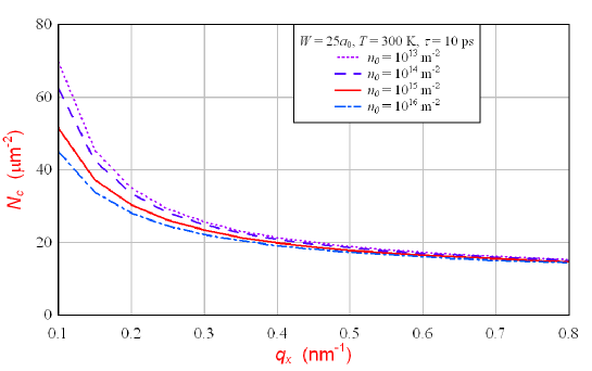
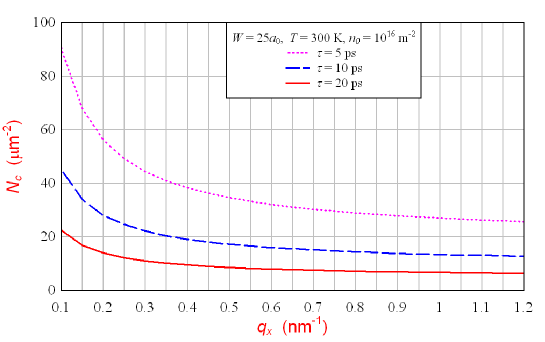
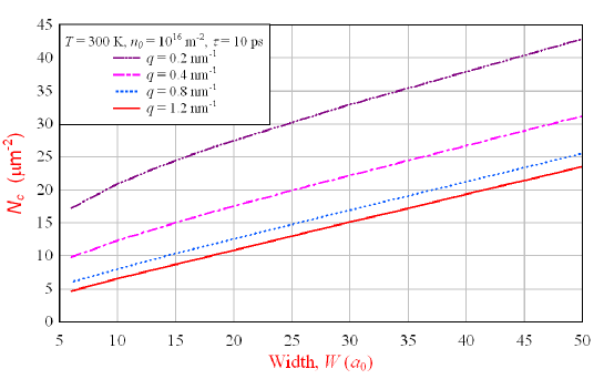
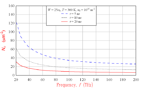
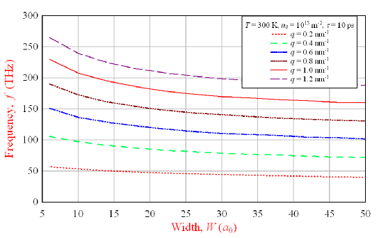
The dependence of the critical density of the QDs required for the amplification of the signal on the wave vector for the different doping electron densities at the fixed width of the nanoribbon, temperature and dissipation time corresponding to the damping, obtained using Eq. (14) is presented in Fig. 1. According to Fig. 1, decreases as and increase. Let us mention that at larger than there is almost no difference between the values of corresponding to the different doping electron densities , and for large converges to approximately . In Fig. 2 the dependence of the critical density of the QDs required for the amplification of the signal on the wave vector for the different dissipation time corresponding to the damping at the fixed width of the nanoribbon, temperature and doping electron densities obtained using Eq. (14) is shown. As it follows from Fig. 2, decreases as and increase. This means that higher damping corresponds to higher . According to Fig. 2, starting with , depends very weakly on , converging to some constant values that depend on the value of . The dependence of the critical density of the QDs required for the amplification of the signal on the width of the nanoribbon at the different wave vector for the fixed dissipation time corresponding to the damping, temperature and doping electron densities obtained using Eq. (14) is displayed in Fig. 3. From Fig. 3 we can conclude that increases as increases and decreases as increases. When increases, the values of stronger depend on . The dependence of the critical density of the QDs required for the amplification of the signal on the frequency at the different dissipation time corresponding to the damping for the fixed temperature and doping electron density obtained using Eq. (14) is shown in Fig. 4. As it is demonstrated in Fig. 4, increases as and decrease. According to Fig. 4, starting with , depends very weakly on frequency and converges to some constant values that depend on the value of . The dependence of the plasmon frequency on the width of the nanoribbon , for the different wave vectors at the fixed dissipation time corresponding to the damping, temperature and doping electron density obtained using Eq. (16) is presented in Fig. 5. According to Fig. 5, the plasmon frequency increases as increases and the width of the nanoribbon decreases. If in Eq. (14), the imaginary part of the dielectric function would not depend on the width , would not depend on . However, due to the complicated dependence of on through given by Eq. (22), this dependence exists. For the damping time we use , , and , because such damping for graphene was obtained in the experimental studies Neugebauer ; Orlita ; Dubinov ; Emani . One can conclude from Figs. 2 and 4, that decreases when the damping time increases.
Let us mention that we used the parameters for PbS and PbSe QDs to calculate , because among different materials for the QDs the PbS and PbSe QDs demonstrate the lowest transition frequency Auxier , which can be in the resonance with the plasmon in graphene nanoribbon in the IR region of spectrum. According to Ref. Plum, , the transition frequency for the QDs depends on the radius of the QDs. The PbS QDs with the radii — have the transition frequencies and Plum . For our calculations we use PbS and PbSe QDs synthesized with the radii up to , which can provide the transition frequency Stockman_QD . Let us mention that changing the radius of the QDs, we can change the frequency of the QDs resonant to the plasmon frequency in graphene nanoribbon controlled by the wave vector , and, therefore, we can control by the radius of the . The density of PbS QDs with the diameter applied for the amplification of plasmons in a gold film in the experiment Plum was . According to Figs. 1-4, in the graphene nanoribbon-based spaser there are possibilities to achieve much less densities of the PbS QDs necessary for amplification than in the gold film-based spaser.
Let us mention that in our calculations we take into account the temporal and spatial dispersion of the dielectric function of graphene nanoribbon in the random phase approximation Brey_Fertig_01 ; Brey_Fertig . The effects of spatial dispersion are very important for the properties of spaser based on a flat metal nanofilm Larkin . Taking into account the spatial dispersion of the dielectric function of a metal surface in the local random phase approximation allows to conclude that the strong interaction of QD with unscreened metal electrons in the surface nanolayer causes enhanced relaxation due to surface plasmon excitation and Landau damping in a spaser based on a flat metal nanofilm Larkin . And we assume that taking into account the spatial dispersion of the dielectric function of graphene nanoribbon is also very important to calculate the minimal population inversion needed for the net SP amplification in the graphene nanoribbon based spaser.
The advantages of the graphene nanoribbon based spaser are wide frequency generation region from THz up to IR, small damping — low threshold for pumping, possibility of control by the gate. While we perform our calculations for IR radiation corresponding to the transition frequencies , the graphene-based spaser can work at the frequencies much below that this one including THz regime.
Acknowledgements.
The authors are grateful to M. I. Stockman for valuable discussions. The work was supported by PSC CUNY under Grant No. 65572-00 43.Appendix A The dielectric function of graphene nanoribbon
For the armchair graphene nanoribbon the dielectric function in the one-band approximation in the random phase approximation is given by Brey_Fertig
| (17) |
where is the Coulomb matrix element, and the polarizability can be approximated by
| (18) |
with
| (19) |
where is the spin degeneracy factor, , is the Boltzmann constant and is the chemical potential controlled by the doping. The chemical potential can be calculated as , where electron concentration is given by and that is the Fermi velocity of electrons in graphene, where is a lattice constant and the value of the overlap integral between the nearest carbon atoms is Lukose .
Let us mention that at we have . The temperature was used in Ref. Brey_Fertig, .
The Coulomb matrix element is given by Brey_Fertig
| (20) |
where is the width of graphene nanoribbon in the direction. The one-dimensional Fourier transform of the Coulomb interaction has the form Li_DasSarma
| (21) |
where is the charge of an electron, is the dielectric constant of graphene, is the zeroth-order modified Bessel function of the second kind, which diverges as when goes to zero.
Appendix B The electric field of a plasmon in a graphene nanoribbon
can be found from the equation:
| (23) |
If there are two materials contacting each other along the plane there are the boundary conditions at the plane of the contact: and , where and are the the normal to the contact plane components of , and and are tangent to the contact plane components of .
Using the notation , , we have
| (24) |
At and we have from Eqs. (23) and (24)
| (25) |
which can be presented as
| (26) |
If we do the Fourier transformation of Eq. (26) and use the property of the Fourier image of the convolution, we obtain
| (27) |
Let us mention that for or or or it is obvious that Eq. (27) follows from Eqs. (23) and (24).
If we define the potential , we obtain from Eq. (27) for and
| (28) |
The solution of Eq. (28) for will be written as
| (29) |
where . Then we have for where
| (30) |
where . From the boundary conditions, we have , , where for the armchair nanoribbon we have from Ref. Brey_Fertig_01, at the width , where is the graphene lattice constant defined above, is the integer. We will use .
References
- (1) D. J. Bergman and M. I. Stockman, Phys. Rev. Lett. 90, 027402 (2003).
- (2) M. I. Stockman, J. Opt. 12, 024004 (2010).
- (3) I. E. Protsenko, Physics-Uspekhi 55, 1040 (2012).
- (4) V. M. Agranovich and V. L. Ginzburg, Crystal Optics with Spartial Dispersion, and Excitons, (Springer, Berlin, 1984).
- (5) Yu. E. Lozovik and A. V. Klyuchnik, The Dielectric Function and Collective Oscillations Inhomogeneous Systems, in The Dielectric Function of Condensed Systems, edited by L. V. Keldysh, D. A. Kirzhnitz, and A. A. Maradudin, p. 299 (Elsevier, Amsterdam, 1987).
- (6) A. V. Zayats, I. I. Smolyaninov, and A. A. Maradudin, Phys. Rep. 408, 131 (2005).
- (7) D. K. Gramotnev and S. I. Bozhevolnyi, Nature Photonics 4, 83 (2010).
- (8) M. I. Stockman, Nature Photonics 2, 327 (2008).
- (9) A. A. Lisyansky, I. A. Nechepurenko, A. V. Dorofeenko, A. P. Vinogradov, and A. A. Pukhov, Phys. Rev. B84, 153409 (2011).
- (10) E. S. Andrianov, A. A. Pukhov, A. V. Dorofeenko, A. P. Vinogradov, and A. A. Lisyansky, Optics Letters 36, 4302 (2011).
- (11) E. S. Andrianov, A. A. Pukhov, A. V. Dorofeenko, A. P. Vinogradov, and A. A. Lisyansky, Optics Express 19, 24849 (2011).
- (12) E. S. Andrianov, A. A. Pukhov, A. V. Dorofeenko, A. P. Vinogradov, and A. A. Lisyansky, Phys. Rev. B85, 035405 (2012).
- (13) E. S. Andrianov, A. A. Pukhov, A. V. Dorofeenko, A. P. Vinogradov, and A. A. Lisyansky, Phys. Rev. B85, 165419 (2012).
- (14) D. G. Baranov, E. S. Andrianov, A. P. Vinogradov, and A. A. Lisyansky, Optics Express 21, 10779 (2013).
- (15) A. Noginov, G. Zhu, V. P. Drachev, and V. M. Shalaev, in Nanophotonics with Surface Plasmons, edited by V. M. Shalaev and S. Kawata (Elsevier, Amsterdam, 2007).
- (16) M. A. Noginov, G. Zhu, A. M. Belgrave, R. Bakker, V. M. Shalaev, E. E. Narimanov, S. Stout, E. Herz, T. Suteewong, and U. Wiesner, Nature 460, 1110 (2009).
- (17) N. I. Zheludev, S. L. Prosvirnin, N. Papasimakis, and V. A. Fedotov, Nature Photonics 2, 351 (2008).
- (18) E. Plum, V. A. Fedotov, P. Kuo, D. P. Tsai, and N. I. Zheludev, Opt. Express 17, 8548 (2009).
- (19) R. A. Flynn, C. S. Kim, I. Vurgaftman, M. Kim, J. R. Meyer, A. J. Mäkinen, K. Bussmann, L. Cheng, F.-S. Choa, and J. P. Long, Opt. Express 19, 8954 (2011).
- (20) L. A. Falkovsky and A. A. Varlamov, Eur. Phys. J. B 56, 281 (2007).
- (21) L. A. Falkovsky and S. S. Pershoguba, Phys. Rev. B76, 153410 (2007).
- (22) L. A. Falkovsky, J. Phys.: Conf. Ser. 129, 012004 (2008).
- (23) F. H. L. Koppens, D. E. Chang, and F. J. G. de Abajo, Nano Lett. 11, 3370 (2011).
- (24) A. H. Castro Neto, F. Guinea, N. M. R. Peres, K. S. Novoselov, and A. K. Geim, Rev. Mod. Phys. 81, 109 (2009).
- (25) S. Das Sarma, S. Adam, E. H. Hwang, and E. Rossi, Rev. Mod. Phys. 83, 407 (2011).
- (26) E. H. Hwang and S. Das Sarma, Phys. Rev. B75, 205418 (2007).
- (27) Yu. E. Lozovik, Physics-Uspekhi, 55, 1035 (2012).
- (28) S. A. Mikhailov, Phys. Rev. B87, 115405 (2013).
- (29) V. G. Kravets, F. Schedin, R. Jalil, L. Britnell, R. V. Gorbachev, D. Ansell, B. Thackray, K. S. Novoselov, A. K. Geim, A. V. Kabashin, and A. N. Grigorenko, Nature Materials 12, 304 (2013).
- (30) L. Brey and H. A. Fertig, Phys. Rev. B73, 235411 (2006).
- (31) L. Brey and H. A. Fertig, Phys. Rev. B75, 125434 (2007).
- (32) V. V. Popov, T. Yu. Bagaeva, T. Otsuji, and V. Ryzhii, Phys. Rev. B81, 073404 (2010).
- (33) O. L. Berman, V. S. Boyko, R. Ya. Kezerashvili, A. A. Kolesnikov, Yu. E. Lozovik, Physics Letters A 374, 4784 (2010).
- (34) O. L. Berman and R. Ya. Kezerashvili, J.Phys.: Condens. Matter 24, 015305 (2012).
- (35) I. E. Tamm, Fundamentals of the Theory of Electricity (Central Books Ltd, 1980).
- (36) L. D. Landau and E. M. Lifshitz, Electrodynamics of Continuous Media (Oxford: Pergamon Press, 1984).
- (37) M. I. Stockman, SPIE Proceedings, 4992, Ultrafast Phenomena in Semiconductors VII, (Eds. K.-T. F. Tsen, J.-J. Song, H. Jiang, pp.60-74, 2003).
- (38) P. Neugebauer, M. Orlita, C. Faugeras, A. L. Barra, and M. Potemski, Phys. Rev. Lett. 103, 136403 (2009).
- (39) M. Orlita and M. Potemski, Semicond. Sci. Technol. 25 063001 (2010).
- (40) A. A. Dubinov, V. Ya. Aleshkin, V. Mitin, T. Otsuji. and V. Ryzhii, J. Phys.: Condens. Matter 23, 145302 (2011).
- (41) N. K. Emani, T.-F. Chung, X. Ni, A. V. Kildishev, Y. P. Chen, and A. Boltasseva, Nano Lett. 12, 5202 (2012).
- (42) Q. P. Li and S. Das Sarma, Phys. Rev. B43, 11768 (1991).
- (43) J. M. Auxier, A. Schülzgen, M. M. Morrell, B. R. West, S. Honkanen, S. Sen, N. F. Borrelli, and N. Peyghambarian, SPIE Proceedings, 5709, Fiber Lasers II: Technology, Systems, and Applications, (Eds. L. N. Durvasula, A. J. W. Brown, J. Nilsson, pp. 249-262, 2005).
- (44) I. A. Larkin, M. I. Stockman, M. Achermann, and V. I. Klimov, Phys. Rev. B69, 121403(R) (2004).
- (45) V. Lukose, R. Shankar, and G. Baskaran, Phys. Rev. Lett. 98, 116802 (2007).