Weak Topological Insulators in PbTe/SnTe Superlattices
Abstract
It is desirable to realize topological phases in artificial structures by engineering electronic band structures. In this paper, we investigate (PbTe)m(SnTe)2n-m superlattices along the [001] direction and find a robust weak topological insulator phase for a large variety of layer numbers and . We confirm this topologically non-trivial phase by calculating topological invariants and topological surface states based on the first-principles calculations. We show that the folding of Brillouin zone due to the superlattice structure plays an essential role in inducing topologically non-trivial phases in this system. This mechanism can be generalized to other systems in which band inversion occurs at multiple momenta, and gives us a brand-new way to engineer topological materials in artificial structures.
pacs:
71.20.-b,73.20.-r,73.21.Cd,71.28.+dI Introduction
The concept of time reversal (TR) invariant topological insulators (TIs) characterizes a new class of materials that are insulating in the interior of a sample, but whose surfaces contain robust conducting channels protected by TR symmetry.Hasan and Kane (2010); Qi and Zhang (2011); Moore (2010); Qi and Zhang (2010) Since the metallic surface states of TIs can be described by Dirac fermions with exotic physical properties, researchers have been interested in pursuing different types of topological materials.Hasan and Kane (2010); Qi and Zhang (2011) TR invariant TIs can exist in both two dimensions and three dimensions. TIs in two dimensions, also known as “quantum spin Hall insulators”, were first predicted theoretically.Kane and Mele (2005); Bernevig and Zhang (2006); Bernevig et al. (2006) The quantum spin Hall effect was experimentally observed in HgTe/CdTe quantum wells (QWs)König et al. (2007) and in InAs/GaSb type II QWs Knez et al. (2011, 2010); Du et al. (2013). In three dimensions, TR invariant TIs can be further classified into two categories, strong TIs and weak TIs.Fu et al. (2007); Fu and Kane (2007); Moore and Balents (2007); Roy (2009a) Strong TIs have an odd number of Dirac cones at their surfaces and can be characterized by one topological invariant, while the surface states of weak TIs contain an even number of Dirac cones and three additional topological invariants are required.Fu and Kane (2007) Strong TIs have been realized experimentally in various classes of materials, including Bi1-xSbx, Fu and Kane (2007); Zhang et al. (2009a); Hsieh et al. (2008) Bi2Se3 family,Zhang et al. (2009b); Chen et al. (2009); Hsieh et al. (2009) family,Chen et al. (2010); Sato et al. (2010) family, Xu et al. (2010); Jin et al. (2011) strained bulk HgTe,Fu et al. (2007); Brüne et al. (2011); Hancock et al. (2011) etc. In contrast, only a few practical systems for weak TIs have been proposed theoretically Yan et al. (2012); Hou et al. (2011); Tang et al. (2013) and no experiments on weak TIs have been reported, up to our knowledge. Surface states of weak TIs are also expected to possess intriguing phenomena, such as one-dimensional helical modes along dislocation lines,Ran et al. (2009) the weak anti-localization effect,Mong et al. (2012) the half quantum spin Hall effect,Liu et al. (2012) etc.Imura et al. (2011, 2012); Yoshimura et al. (2013); Ringel et al. (2012); Fulga et al. (2012); Fu and Kane (2012) Impurity scattering is reduced for surface states of TIs, so electric currents can flow with low dissipation. This leads to wide-ranging interests in device applications of TIs.
To search for new topological materials with robust physical properties, it is essential to engineer electronic band structures with the desired features. A useful and intuitive physical picture to understand TIs is the concept of “band inversion”. Band inversion means that the band orderings of conduction and valence bands are changed at some high symmetry momenta in the Brillouin zone (BZ), so that band dispersion cannot be adiabatically connected to the atomic limit of the system under certain symmetries.Roy (2009b); Fu and Kane (2007); Bernevig et al. (2006) In other words, the band gap changes its sign from positive to negative when band inversion occurs (We usually define the sign of a normal band gap to be positive). Actually all the well-known topological materials have “inverted” band structures. A large variety of experimental methods can be applied to tune band gaps, such as controlling chemical compositions by doping,Hsieh et al. (2008); Dziawa et al. (2012); Sato et al. (2013) applying strain,Brüne et al. (2011) etc. In this paper, we propose that band inversion can be controlled by constructing superlattice structures, which has the obvious advantage of their controllability. We will consider the PbTe/SnTe superlattice, a typical semiconductor superlattice made of IV-VI group compounds, as an example due to its simplicity. We will show that weak TIs can be achieved for PbTe/SnTe superlattices grown along the [001] direction. Remarkably, the weak TI phase we found is not equivalent to a stack of 2D quantum spin Hall layers in [001] direction. Instead, the nontrivial topology arises from the folding of BZ, which plays an essential role in inducing band inversion. This mechanism can be in principle generalized to search for other topological phases, including strong TIs and topological crystalline insulators, and paves the way to engineering topological phases in artificial structures.
This paper is organized in the following way. In section II, we briefly review the bulk properties of PbTe and SnTe, and introduce our calculation methods. In section III, we will show the evolution of band structure from PbTe to a superlattice step by step to illustrate how we obtain weak TIs. We calculate topological invariants, as well as surface states of the superlattice, to demonstrate the weak TI phase in this system. We will also discuss experimental realization and other possibilities to realize weak TI based on the same mechanism. The conclusion is drawn in section IV.
II Superlattice configuration and calculation methods
We start with a review of material properties of bulk PbTe and SnTe. PbTe and SnTe have face-centered cubic NaCl-type of structures with the corresponding BZ shown in Fig. 1. Both materials are narrow gap semiconductors with multiple applications in thermoelectricity, infrared diode and even superconductivityWei and Zunger (1997); Hummer et al. (2007); Svane et al. (2010). The band gaps of these materials are located at the center of the hexagon on the BZ boundary, usually denoted as L points (See Fig. 1(b)). There are four L points in totel, which are related to each other by mirror symmetry. It was shown that the band gap of SnTe has the opposite sign of that of PbTe.Hsieh Timothy H.and Lin et al. (2012) Consequently, the systems consisting of SnTe and PbTe may possess topologically non-trivial properties. For example, recent interest in these IV-VI semiconductors is stimulated by the prediction that SnTe represents a new type of topological phase dubbed “topological crystalline insulators”, which host gapless surface states protected by mirror symmetry. Fu (2011); Hsieh Timothy H.and Lin et al. (2012); Fang et al. (2012); Slager et al. (2012); Liu et al. (2013) This finding was recently confirmed by the experimental observation of surface states in SnTe family of materials.Tanaka et al. (2012); Xu et al. (2012); Dziawa et al. (2012) With additional uniaxial strain along the [111] direction, both PbTe and SnTe are expected to be strong TIs.Fu and Kane (2007); Lin et al. (2010) A more recent theoretical work Buczko and Cywiński (2012) shows that, in a large thickness range, PbTe/SnTe superlattice along the [111] direction exhibit properties similar to a strong TI phase. In this work, we will consider a superlattice with alternative stacks of SnTe and PbTe layers along the [001] direction, denoted as (PbTe)m(SnTe)2n-m, where and represent the number of PbTe and SnTe layers, respectively. Fig. 1(a) shows the (PbTe)1(SnTe)1 superlattice as an example.
The calculations are performed within the framework of density functional theory (DFT) calculations using the Perdew-Burke-Ernzerhof (PBE) generalized gradient approximationPerdew et al. (1996) and the projector augmented wave (PAW) potentialBlöchl (1994), as implemented in the Vienna ab initio simulation package (VASP)Kresse and Furthmüller (1996). The spin-orbit coupling is included in all the calculations. The energy cutoff of the plane-wave basis is 340 eV. The 101010 and 10101 Monkhorst-Pack k points are used for bulk and surface calculations separately. The lattice parameters are obtained by structural optimization.
Different topological phases can be determined by calculating topological invariants.Fu and Kane (2006, 2007) In three dimensions, there are four topological invariants, one strong topological index and three weak topological indices. With space inversion symmetry preserved, topological invariants can be evaluated easily using the parity of occupied states at eight time-reversal-invariant momenta (TRIM) ().Fu and Kane (2007) The strong topological index is given by
| (1) |
and the three weak topological indices are given by
| (2) |
where is the product of parity of all occupied states for one time-reversal copy at TRIM and are the reciprocal lattice vectors.Fu and Kane (2007) A strong TI phase is determined by the index while a weak TI phase is characterized by a vector . Weak TIs can be understood as a stacking of 2D TI layers along the direction .Fu and Kane (2007) On the surfaces with miller index in weak TIs, an even number of Dirac surface states can appear.Fu and Kane (2007) As a check of our numerical methods, we calculate the parity of all occupied states at TRIM for the bulk SnTe and PbTe, as shown in Table 1. As expected, both strong topological index and weak topological indices are trivial for SnTe and PbTe, which is consistent with the previous analysis.Fu and Kane (2007) The underlying reason is that there are four L points with for SnTe and for PbTe (), as shown in Table 1. However, since both strong topological index (1) and weak topological indices (2) contain an even number of L points, the product of always gives a sign. Therefore, in order to achieve topological non-trivial phases, it is essential to reduce the number of equivalent L points, which can be achieved by a superlattice structure, as discussed in detail below.
| PbTe | ||
| 1 | ||
| 3X | ||
| 4L | ||
| index | (0;000) | |
| SnTe | ||
| 1 | ||
| 3X | ||
| 4L | + | |
| index | (0;000) |
III Weak topological insulators in PbTe/SnTe superlattices
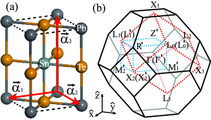
The band structure of a PbTe/SnTe superlattice can be understood from a simple physical picture in two steps. Let us consider the (PbTe)1(SnTe)1 superlattice along the [001] direction as an example. The first step is to transform from the primitive cell of bulk PbTe to the superlattice cell along the [001] direction. The corresponding primitive lattice vectors are changed from of a face-centered cubic lattice, where is the distance between Pb and nearest Te atom, to for the superlattice cell, as shown in Fig. 1(a). Since the superlattice cell is twice the primitive cell, the corresponding BZ of the superlattice is folded and becomes half the original one. As shown in Fig. 1, eight TRIM (, 3X, 4L) are transformed to four TRIM () in the folded BZ: and is projected to a single point , and to , and L3 to , L1 and L2 to . Besides, there will be four new TRIM in the folded BZ, denoted as in Fig. 1(b). Since the BZ is reduced, band dispersion should also be folded (see Fig. 2(a)). Consequently, the s in the folded BZ are just the product of the at the corresponding TRIM in the original BZ, e.g. . The new emerging TRIM are at the boundary of the folded BZ, so one can combine the wavefunction at with that at to form the bonding and anti-bonding states that are the eigenstates of inversion operation. Since the bonding and anti-bonding states have opposite parities, the s at these new TRIM take the value of . Thus, from () and (), one finds that both strong topological index and weak topological indices remain unchanged, which is expected since the lattice remains the same in this step.
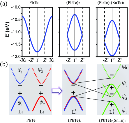
Next, we substitute one Pb atom by one Sn atom in the superlattice cell as shown in Fig. 1(a). This does not break inversion symmetry and thus we can still use Eqs. (1) and (2) to evaluate topological invariants. Introducing Sn atoms induces the interaction between the states at and splits the degeneracy. When the splitting is large enough, band inversion occurs at these momenta. In Fig. 2(b), we denote the wavefunctions of conduction bands as (odd parity) and those of valence bands as (even parity) at L1,2. After replacing atoms, both and are no longer the eigen-states of the (PbTe)1(SnTe)1 superlattice and they will hybridize to form new eigenstates and , as shown in Fig. 2(b). Due to level repulsion, the state of the valence band maximum will be pushed up while the state of the conduction band minimum will be pushed down. Since and have opposite parities, band inversion occurs when and change their sequences, as shown in the second step of Fig. 2(b). A similar situation happens at L. Thanks to reduction in the number of L points from four to two in the first step, the band inversion at can lead to a weak TI phase in PbTe/SnTe superlattices. The replacement by Sn atoms will also split the degeneracy at TRIM , as shown in Fig. 2(a). However, since the initial gaps at these TRIM are huge, the splitting will not change any band sequences. It should be emphasized that this mechanism does not rely on the inverted band structure of SnTe. Instead, band inversion originates from the strong coupling between the states at equivalent L points due to the folding of the BZ in a superlattice structure.
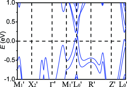
Therefore, the replacement of Pb atoms by Sn atoms will change the sign of and but leave the and at other TRIM unchanged. Strong topological index should still be zero since there are always even number times of band inversion. Nevertheless, weak topological indices can be nonzero, so we carry out an ab initio calculation for the (PbTe)1(SnTe)1 superlattice and the energy dispersion is shown in Fig. 3. A Mexican-hat shape of dispersion appears around L, indicating the occurrence of band inversion. Furthermore, we check the at all TRIM and , as shown in the table 2. We find the weak TI indices , so the present system can be viewed as a stacking of two dimensional TIs along x direction. ( Since , , are the reciprocal lattice vectors for the (PbTe)1(SnTe)1 superlattice, equals ).
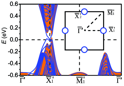
For a weak TI with , surface states with even number of Dirac cones are expected on the surface with Miller index . Thus, we consider a slab configuration of (PbTe)1(SnTe)1 superlattice along [001] direction and directly calculate surface states with the ab initio method. Indeed, as shown in Fig. 4, surface states are found around , which is the projection of at the surface BZ of the superlattice. The Dirac point is located exactly at TRIM (The tiny gap of surface states at is due to the finite size effect of a slab configuration). According to the mirror symmetry or the four-fold rotation symmetry that relates to , we expect another Dirac point at TRIM . The degeneracy at is protected by TR symmetry according to Kramers’ theorem. Therefore, our calculation of topological surface states is consistent with the analysis of bulk topological invariants, confirming that the (PbTe)1(SnTe)1 superlattice is a weak TI. Similar to the case of strong TIs, the backscattering in one Dirac cone is completely suppressed due to the helical nature of spin texture. Since two points are well separated in momentum space, the scattering between two Dirac cones is negligible for impurities with smooth pontentials.
Remarkably, the surface states here are qualitatively different from the surface states of SnTe, which consist of four Dirac points at non-TRIM and are protected by mirror symmetry instead of TR symmetry. For the (PbTe)1(SnTe)1 superlattice, mirror symmetry can also play a role. Actually, there is additional protection of the gapless Dirac points at and by the mirror symmetry with respect to plane (the plane along the line in Fig. 4 and perpendicular to the surface) and (110) plane (the plane along the line in Fig. 4), respectively. Since there is only one Dirac cone at one mirror plane, the mirror Chern number should be in the present system , in contrast to in bulk SnTe. Therefore, the (PbTe)1(SnTe)1 superlattice can also be regarded as a TCI with mirror Chern number 1. When TR symmetry is broken but mirror symmetry is preserved, e.g. with an in-plane magnetic field along the [1] or [110] direction, the gapless nature of Dirac cones should still remain.
3D weak TIs are usually constructed by stacking 2D TIs, such as layered semiconductors discussed in Ref. [Yan et al., 2012; Tang et al., 2013]. In these cases, if we take the stacking direction as direction, the corresponding weak topological indices are . In contrast, the weak topological indices of our system are different from the growth direction of superlattices. Thus, the underlying mechanism of our system is not the stacking of 2D TIs, but the folding of BZ, as discussed above. In our system, two surface Dirac cones appearing at and of surfaces are related to each other by four-fold rotation symmetry or mirror symmetry. When there is scattering between two Dirac cones, charge density waves can occur at (001) surfaces, giving rise to the half quantum spin Hall effect proposed in Ref. [Liu et al., 2012].
| X | ||
| Z′ | ||
| R′ | ||
| index | (0;110) |
Similar discussion can also be applied to other (PbTe)m(SnTe)2n-m superlattices ( and are integers) and it turns out that the weak TI phase is quite robust. The BZ of (PbTe)m(SnTe)2n-m superlattice can be obtained by simply folding the BZ of a (PbTe)1(SnTe)1 superlattice along the z direction. Two L′ points in a (PbTe)1(SnTe)1 superlattice will be still mapped to two separate TRIM in the new BZ. Thus, the machanism for the weak TI phase is still applicable. As shown in Table 3, for a large range of the ratio , the system keeps in the weak TI phase with and the corresponding band gaps vary around tens of meV. Thus, a fine tuning of layer numbers of the superlattice is not necessary. Similar superlattices have been fabricated in early experiments. Springholz (2013); Fujiyasu et al. (1984); Kriechbaum et al. (1984); Ishida et al. (1985) Therefore, PbTe/SnTe superlattices along the [001] direction provide us an experimentally feasible and controllable platform to investigate the exotic phenomena of weak TIs. Moreover, since our basic mechanism is quite general, it is also worthwhile to investigate GeTe/SnTe Barone et al. (2013) and PbSe/SnSe superlatticesDziawa et al. (2012).
| Composition | Gap at (meV) | Bulk Gap (meV) |
|---|---|---|
| 370.8 | 33.0 | |
| 144.6 | 31.8 | |
| 154.6 | 1.0 | |
| 87.9 | 26.5 | |
| 96.9 | 27.5 | |
| 69.0 | 17.6 |
IV Conclusion
In summary, we propose a series of superlattice systems to realize weak TIs. Due to the BZ folding, we reduce the number of equivalent L points so that weak TI phases can be realized in PbTe/SnTe superlattices, which cannot be achieved in the bulk PbxSn1-xTe with uniform doping. We notice that the PbTe/SnTe superlattice along the [111] direction has been investigated with the effective Hamiltonian at four equivalent L points.Buczko and Cywiński (2012) In this case, four L points are projected into different momenta in the folded BZ, so that they can be treated separately and the effect of BZ folding is not important. But for the superlattice along the [001] direction, different L points will be mapped to the same momentum in the folded BZ. Therefore, the coupling between different L points cannot be neglected and instead shows a new mechanism to engineer topological phases. This idea can be generalized to search for new topological phases in other systems where band gap occurs at several equivalent momenta.
Acknowledgements.
We acknowledge support from the Ministry of Science and Technology of China (Grant Nos. 2011CB921901 and 2011CB606405) and the National Natural Science Foundation of China (Grant No. 11074139). LF is supported by the DOE Office of Basic Energy Sciences, Division of Materials Sciences and Engineering under award DE-SC0010526.References
- Hasan and Kane (2010) M. Z. Hasan and C. L. Kane, Rev. Mod. Phys. 82, 3045 (2010).
- Qi and Zhang (2011) X.-L. Qi and S.-C. Zhang, Rev. Mod. Phys. 83, 1057 (2011).
- Moore (2010) J. E. Moore, Nature 464, 194 (2010).
- Qi and Zhang (2010) X. L. Qi and S. C. Zhang, Phys. Today 63, 33 (2010).
- Kane and Mele (2005) C. L. Kane and E. J. Mele, Phys. Rev. Lett. 95, 226801 (2005).
- Bernevig and Zhang (2006) B. A. Bernevig and S.-C. Zhang, Phys. Rev. Lett. 96, 106802 (2006).
- Bernevig et al. (2006) B. A. Bernevig, T. L. Hughes, and S.-C. Zhang, Science 314, 1757 (2006).
- König et al. (2007) M. König, S. Wiedmann, C. Brüne, A. Roth, H. Buhmann, L. W. Molenkamp, X.-L. Qi, and S.-C. Zhang, Science 318, 766 (2007).
- Knez et al. (2011) I. Knez, R.-R. Du, and G. Sullivan, Phys. Rev. Lett. 107, 136603 (2011).
- Knez et al. (2010) I. Knez, R. R. Du, and G. Sullivan, Phys. Rev. B 81, 201301 (2010).
- Du et al. (2013) L. Du, I. Knez, G. Sullivan, and R.-R. Du, ArXiv e-prints (2013), eprint 1306.1925.
- Fu et al. (2007) L. Fu, C. L. Kane, and E. J. Mele, Phys. Rev. Lett. 98, 106803 (2007).
- Fu and Kane (2007) L. Fu and C. L. Kane, Phys. Rev. B 76, 045302 (2007).
- Moore and Balents (2007) J. E. Moore and L. Balents, Phys. Rev. B 75, 121306 (2007).
- Roy (2009a) R. Roy, Phys. Rev. B 79, 195322 (2009a).
- Zhang et al. (2009a) H.-J. Zhang, C.-X. Liu, X.-L. Qi, X.-Y. Deng, X. Dai, S.-C. Zhang, and Z. Fang, Phys. Rev. B 80, 085307 (2009a).
- Hsieh et al. (2008) D. Hsieh, D. Qian, L. Wray, Y. Xia, Y. S. Hor, R. J. Cava, and M. Z. Hasan, Nature 452, 970974 (2008).
- Zhang et al. (2009b) H.-J. Zhang, C.-X. Liu, X.-L. Qi, X. Dai, Z. Fang, and S.-C. Zhang, Nat Phys. 5, 438 (2009b).
- Chen et al. (2009) Y. L. Chen, J. G. Analytis, J.-H. Chu, Z. K. Liu, S.-K. Mo, X. L. Qi, H. J. Zhang, D. H. Lu, X. Dai, Z. Fang, et al., 325, 178 (2009).
- Hsieh et al. (2009) D. Hsieh, Y. Xia, D. Qian, L. Wray, F. Meier, J. H. Dil, J. Osterwalder, L. Patthey, A. V. Fedorov, H. Lin, et al., Phys. Rev. Lett. 103, 146401 (2009).
- Chen et al. (2010) Y. L. Chen, Z. K. Liu, J. G. Analytis, J.-H. Chu, H. J. Zhang, B. H. Yan, S.-K. Mo, R. G. Moore, D. H. Lu, I. R. Fisher, et al., Phys. Rev. Lett. 105, 266401 (2010).
- Sato et al. (2010) T. Sato, K. Segawa, H. Guo, K. Sugawara, S. Souma, T. Takahashi, and Y. Ando, Phys. Rev. Lett. 105, 136802 (2010).
- Xu et al. (2010) S.-Y. Xu, L. A. Wray, Y. Xia, R. Shankar, A. Petersen, A. Fedorov, H. Lin, A. Bansil, Y. S. Hor, D. Grauer, et al., ArXiv e-prints (2010), eprint 1007.5111.
- Jin et al. (2011) H. Jin, J.-H. Song, A. J. Freeman, and M. G. Kanatzidis, Phys. Rev. B 83, 041202 (2011).
- Brüne et al. (2011) C. Brüne, C. X. Liu, E. G. Novik, E. M. Hankiewicz, H. Buhmann, Y. L. Chen, X. L. Qi, Z. X. Shen, S. C. Zhang, and L. W. Molenkamp, Phys. Rev. Lett. 106, 126803 (2011).
- Hancock et al. (2011) J. N. Hancock, J. L. M. van Mechelen, A. B. Kuzmenko, D. van der Marel, C. Brüne, E. G. Novik, G. V. Astakhov, H. Buhmann, and L. W. Molenkamp, Phys. Rev. Lett. 107, 136803 (2011).
- Yan et al. (2012) B. Yan, L. Müchler, and C. Felser, Phys. Rev. Lett. 109, 116406 (2012).
- Hou et al. (2011) J.-M. Hou, W.-X. Zhang, and G.-X. Wang, Phys. Rev. B 84, 075105 (2011).
- Tang et al. (2013) P. Tang, B. Yan, W. Cao, S.-C. Wu, C. Felser, and W. Duan, ArXiv e-prints (2013), eprint 1307.8054.
- Ran et al. (2009) Y. Ran, Y. Zhang, and A. Vishwanath, Nat Phys 5, 298303 (2009).
- Mong et al. (2012) R. S. K. Mong, J. H. Bardarson, and J. E. Moore, Phys. Rev. Lett. 108, 076804 (2012).
- Liu et al. (2012) C.-X. Liu, X.-L. Qi, and S.-C. Zhang, Physica E: Low-dimensional Systems and Nanostructures 44, 906 (2012).
- Imura et al. (2011) K.-I. Imura, Y. Takane, and A. Tanaka, Phys. Rev. B 84, 035443 (2011).
- Imura et al. (2012) K.-I. Imura, M. Okamoto, Y. Yoshimura, Y. Takane, and T. Ohtsuki, Phys. Rev. B 86, 245436 (2012).
- Yoshimura et al. (2013) Y. Yoshimura, A. Matsumoto, Y. Takane, and K.-I. Imura, Phys. Rev. B 88, 045408 (2013).
- Ringel et al. (2012) Z. Ringel, Y. E. Kraus, and A. Stern, Phys. Rev. B 86, 045102 (2012).
- Fulga et al. (2012) I. C. Fulga, B. van Heck, J. M. Edge, and A. R. Akhmerov, ArXiv e-prints (2012), eprint 1212.6191.
- Fu and Kane (2012) L. Fu and C. L. Kane, Phys. Rev. Lett. 109, 246605 (2012).
- Roy (2009b) R. Roy, Phys. Rev. B 79, 195321 (2009b).
- Dziawa et al. (2012) P. Dziawa, B. J. Kowalski, K. Dybko, R. Buczko, A. Szczerbakow, M. Szot, E. tusakowska, T. Balasubramanian, B. M. Wojek, M. H. Berntsen, et al., Nat Mater 11, 10231027 (2012).
- Sato et al. (2013) T. Sato, Y. Tanaka, K. Nakayama, S. Souma, T. Takahashi, S. Sasaki, Z. Ren, A. A. Taskin, K. Segawa, and Y. Ando, Phys. Rev. Lett. 110, 206804 (2013).
- Wei and Zunger (1997) S.-H. Wei and A. Zunger, Phys. Rev. B 55, 13605 (1997).
- Hummer et al. (2007) K. Hummer, A. Grüneis, and G. Kresse, Phys. Rev. B 75, 195211 (2007).
- Svane et al. (2010) A. Svane, N. E. Christensen, M. Cardona, A. N. Chantis, M. van Schilfgaarde, and T. Kotani, Phys. Rev. B 81, 245120 (2010).
- Hsieh Timothy H.and Lin et al. (2012) H. Hsieh Timothy H.and Lin, J. Liu, W. Duan, B. Arun, and L. Fu, Nat Commun 3 (2012).
- Fu (2011) L. Fu, Phys. Rev. Lett. 106, 106802 (2011).
- Fang et al. (2012) C. Fang, M. J. Gilbert, and B. A. Bernevig, Physical Review B 86, 115112 (2012).
- Slager et al. (2012) R.-J. Slager, A. Mesaros, V. Juričić, and J. Zaanen, Nature Physics 9, 98 (2012).
- Liu et al. (2013) J. Liu, W. Duan, and L. Fu, arXiv:1304.0430 (2013).
- Tanaka et al. (2012) Y. Tanaka, Z. Ren, T. Sato, K. Nakayama, S. Souma, T. Takahashi, K. Segawa, and Y. Ando, Nat Phys 8 (2012).
- Xu et al. (2012) S.-Y. Xu, C. Liu, N. Alidoust, M. Neupane, D. Qian, I. Belopolski, J. Denlinger, Y. Wang, H. Lin, L. Wray, et al., Nature communications 3, 1192 (2012).
- Lin et al. (2010) H. Lin, R. S. Markiewicz, L. A. Wray, L. Fu, M. Z. Hasan, and A. Bansil, Phys. Rev. Lett. 105, 036404 (2010).
- Buczko and Cywiński (2012) R. Buczko and L. Cywiński, Phys. Rev. B 85, 205319 (2012).
- Perdew et al. (1996) J. P. Perdew, K. Burke, and M. Ernzerhof, Phys. Rev. Lett. 77, 3865 (1996).
- Blöchl (1994) P. E. Blöchl, Phys. Rev. B 50, 17953 (1994).
- Kresse and Furthmüller (1996) G. Kresse and J. Furthmüller, Phys. Rev. B 54, 11169 (1996).
- Fu and Kane (2006) L. Fu and C. L. Kane, Phys. Rev. B 74, 195312 (2006).
- Springholz (2013) G. Springholz, in Molecular Beam Epitaxy (Elsevier, Oxford, 2013), pp. 263 – 310.
- Fujiyasu et al. (1984) H. Fujiyasu, A. Ishida, H. Kuwabara, S. Shimomura, S. Takaoka, and K. Murase, Surface Science 142, 579 (1984).
- Kriechbaum et al. (1984) M. Kriechbaum, K. E. Ambrosch, E. J. Fantner, H. Clemens, and G. Bauer, Phys. Rev. B 30, 3394 (1984).
- Ishida et al. (1985) A. Ishida, M. Aoki, and H. Fujiyasu, Journal of Applied Physics 58, 1901 (1985).
- Barone et al. (2013) P. Barone, T. c. v. Rauch, D. Di Sante, J. Henk, I. Mertig, and S. Picozzi, Phys. Rev. B 88, 045207 (2013).