Electronic Structure and Upper Critical Field of Superconducting Ta2PdS5
Abstract
We report electronic structure calculations for Ta2PdS5, which is a layered superconductor containing heavy elements and displaying an upper critical field, , 3 times higher than the estimated Pauli limit. We show that this is a multiband superconductor that is most likely in the strong coupling regime. This provides an alternative explanation to strong spin orbit scattering for the high upper critical field.
pacs:
74.20.Rp,74.20.Pq,74.70.DdI introduction
Lu and co-workers Lu et al. (2013) recently reported fully gapped type-II superconductivity with up to 6 K in the layered chalcogenide Ta2PdxS5, 1.0. Remarkably, they found anisotropic upper critical fields, , up to 31 T. This is substantially above the estimated Pauli limit of 10 T. They argued that the high critical fields are the result of strong spin-orbit scattering associated with Pd vacancies.
The purpose of this paper is to present the electronic structure in relation to the experimental findings and in particular the high upper critical field. We find that the compound is a three dimensional low carrier density metal, with moderate anisotropy and a Fermi surface structure that can support multiband superconductivity. This is qualitatively similar to the findings of recent studies of the niobate superconductors, Nb2Pd0.81S5 and Nb3Pd0.7Se7, which also show high upper critical fields. Zhang et al. (2013a, b) A comparison of the calculated density of states with the experimental suggests this compound is in the strong coupling regime. Multiband, strong coupling superconductivity provides and alternative to the proposed spin orbit scattering explanation of the observed high values.
II approach and structure
The present calculations were done for the stoichiometric compound. They were based on density functional theory, using the generalized gradient approximation (GGA) of Perdew, Burke and Ernzerhof (PBE). Perdew et al. (1996) For this purpose we used the general potential linearized augmented planewave (LAPW) method, Singh and Nordstrom (2006) as implemented in the WIEN2k code. Blaha et al. (2001) We used well converged basis sets including local orbitals to treat the semicore states with LAPW sphere radii of 2.25 bohr and 2.1 bohr, for the metal and S atoms, respectively. We used the lattice parameters measured by Lu and co-workers, Lu et al. (2013) and relaxed the atomic positions in the cell by total energy minimization. This relaxation was done with relativity included at the scalar level. Once the atomic positions were obtained, the electronic structure was calculated relativistically, including spin-orbit.
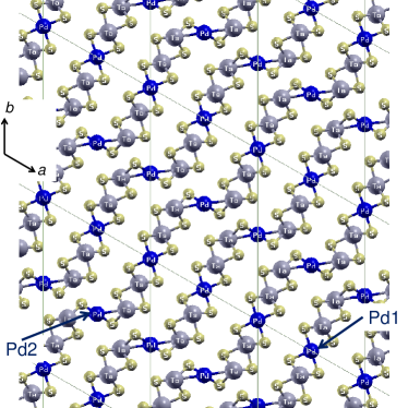
Ta2PdS5 is made up of corrugated metal sulfide sheets as shown in Fig. 1. The crystal structure is centrosymmetric, space group No. 12 (), two formula units per primitive cell, and contains two different Pd sites, Pd1 and Pd2 as well as two different Ta (Ta1 and Ta2) and five different S sites. All the metal sites form chains along the -axis direction, with spacing of =3.269 Å. In the following we use the standard setting, which differs from the setting used in Ref. Lu et al., 2013. In particular, the high conductivity direction, labeled as the -axis, in Ref. Lu et al., 2013, is the -axis direction with the setting used here.
The structure may be described starting with the Pd1 atoms. These are nearly square planar coordinated by S. These near squares are stacked along the -axis direction, with a spacing of =3.269 Å, and edges perpendicular and parallel to the flat part of the sheets shown in Fig. 1 (i.e. S above and below the sheet).
The Ta1 and Ta2 atoms are also in chains along the -axis direction, with the Ta1 chains adjacent to the Pd1 and the Ta2 at the edge of the flat parts of the sheets. Along the -axis the Ta1 are between the Pd1S4 squares, and each of the S in these squares then bonds to two Ta1 atoms and one Pd1. The Ta1 site is six fold coordinated by S. Four of these are from the Pd1S4 squares, and two are shared with the Ta2 sites, completing the flat parts of the sheets. The Pd2 site is on the step part of the corrugated sheets and is also in an approximately square planar coordinated site, but in the S coordinating the Pd2 are shared between Pd2 atoms along the -axis chains. Each of these S is shared between two Pd2 atoms, and is also bonded to two of the Ta2 atoms. This leads to longer S-Pd2 bond lengths of 2.42 Å, as compared to the Pd1-S distances of 2.33 Å. These edges also connect the sheets because of relatively short S-S distances. Experimentally, the Pd2 site has a variable number of random vacancies.
III results and discussion
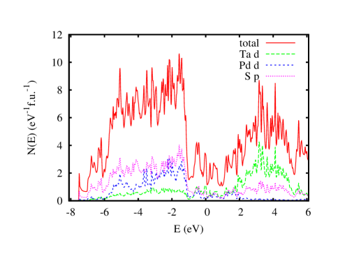
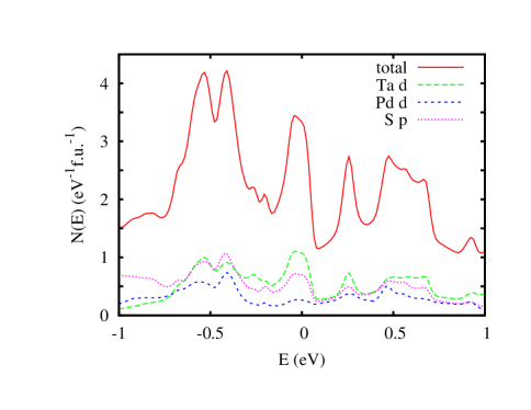
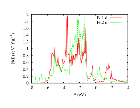
We begin by presenting the electronic density of states (DOS). The calculated electronic density of states and projections onto the various sites are shown in Fig. 2. As may be seen, there is strong covalency between the Ta and various S states. The Pd contribution to the electronic structure is mostly in the occupied bands. However, each Pd contributes one band that is split off above the main Pd density of states. This band has Pd - S antibonding character and is mirrored by corresponding bonding states at the bottom of the Pd DOS (note that this bonding character is spread between several hybridized bands). In any case, this structure, with the antibonding band above the Fermi level, reflects the bonding of the Pd to the S comprising the square planes.
The Pd1 - S antibonding band mentioned above extends from 1 eV to 1.9 eV above the Fermi energy, . In contrast for the Pd2 site, the antibonding band is broader and partially occupied extending from -1 eV to 1 eV, with respect to . This partial occupation of the antibonding band means that the Pd2-S bonding is weaker than the Pd1-S bonding, which may explain why the Pd2 site is susceptible to vacancies. It also means that while the electronic structure near , relevant to transport and superconductivity, has mainly hybridized Ta - S character, it also includes a significant Pd2 - S antibonding contribution. In contrast, there is very little Pd1 character near .
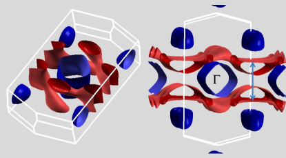
The calculated Fermi surface is shown in Fig. 3. It consists of three sheets. The first is a hole sheet that consists of flattened cylinders running along zone boundary in the direction, with complex interconnection across the zone. The outer parts of the cylinder are flat indicating a nesting at the vector that connects the these, as shown in the figure (but note that the strong defect scattering related to Pd2 vacancies in this material may obscure this nesting).
This hole sheet is compensated by two electron sheets. These are a very two dimensional cylinder around the zone center and small closed sections on the zone faces as shown. This characteristic of compensating hole and electron Fermi surfaces is somewhat reminiscent of the Fe-based superconductors. Singh and Du (2008) However, there is good experimental evidence that the physics here is very different, and specifically that Ta2PdxS5 is an -wave electron phonon superconductor. Lu et al. (2013)
The calculated DOS at the Fermi energy, =3.34 eV-1 on a per formula unit basis. According to the Sommerfeld formula, , this corresponds to a bare specific heat coefficient, =7.88 mJ/(mol K2) again per formula unit. Comparing with the experimentally reported value, =27.6 mJ/(mol K2) one may estimate a specific heat enhancement, (1+)=/=3.5, or 2.5. An electron phonon coupling in this range characterizes Ta2PdxS5 as a strong coupling superconductor. Strong coupling superconductors have a larger ratio of the gap to the critical temperature, i.e. , above the weak coupling (BCS) value and renormalization of the normal state, both of which can increase the higher Pauli limit on the upper critical field. Clogston (1962); Rainer et al. (1973); Orlando et al. (1979) Using the formula, , from Ref. Orlando et al., 1979, and setting the parameter , which is larger than unity, to unity, one obtains a low estimate of the strong coupling Pauli limit, as 1.9 times the weak coupling BCS value . Thus, based on this analysis, it is quite likely that strong coupling effects in Ta2PdS5 can readily yield a factor of two or more increase in the Pauli paramagnetic limit, with no further considerations.
The conductivity anisotropy as obtained in the constant scattering time approximation (CSTA) with the BoltzTraP code, Madsen and Singh (2006) shows that the in-plane anisotropy is weak. The lowest conductivity direction is predicted to be close to the -axis, across the layers. If the scattering rate is independent of direction, as is typically valid in metals, the average conductivity in the high conductivity - plane will be 2.3 times larger than in the -direction, and have little anisotropy itself. The highest conductivity direction is predicted to be , which is the direction of the metal chains, but only by 2% compared to the highest conductivity direction in the - plane. This may be sensistive to disorder due to Pd2 vacancies, which would affect the --plane more than the -axis direction. In any case, the result is consistent with the inference of Lu and co-workers (note that the -axis here is the same as the -axis in the setting used by Lu and co-workers). Lu et al. (2013) Lu and co-workers found the highest along this direction (-axis as defined here), Lu et al. (2013) which is consistent with the fact that it is the high conductivity direction.
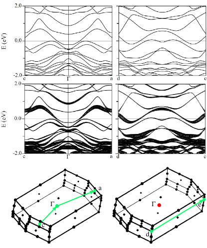
However, the experimental anisotropy of 2.3 is larger than that which would be expected from a single band based on the conductivity anisotropy, i.e. . In a very dirty material with very strong point defect scattering, the assumption of the CSTA, that all bands have scattering with the same scattering rate, may not be valid. On the one hand the band structure shows that the hole band has a pudding mold shape (see especially the right panel of Fig. 4) that places very close to the band edge. This suggests that this band and the small electron pockets on the zone faces could be easily Anderson localized (this is controlled by the the strength of the disorder potential relative to energy distance of the band edge from the Fermi energy). Lee and Ramakrishnan (1985) This would increase the relative contribution of the rather 2D electron cylinder at the zone center to transport and thereby increase the anisotropy.
On the other hand, if the strength of the scattering is not enough to produce Anderson localization but the point defect scattering is still very strong in the strength of providing a mean free path set by the defect spacing, it could be that the mean free path, for the different bands may become similar. If that is the case in the samples of Ta2PdxS5 that were reported, the lighter electron cylinder section of the Fermi surface would be less dominant in the conductivity. In any case, from a transport point of view, Ta2PdS5 should be classed as a three dimensional metal, with a moderate planar anisotropy. It will be of interest to perform transport measurements to determine the conductivity anisotropy in relation to the CSTA results, if suitable superconducting samples can be prepared.
Returning to the Fermi surfaces, the band structure along directions cutting the different sheets and the Pd2 character are shown in Fig. 4. Both the electron and hole sections come from bands of hybridized Ta and S character. However, the band giving rise to the hole cylinder around the zone center shows much stronger dispersion than the that comprising the electron sections. Of the three sections of Fermi surface, the small electron ellipsoids on the zone faces have the highest Pd2 character. This combined with there small size may make them particularly sensitive to Pd2 vacancy induced disorder.
In any case, superconductivity is likely to be dominated by the two larger sheets. While, as mentioned, there is little in plane anisotropy for the total conductivity the individual band anisotropies are different. For the -axis (low conductivity direction) the electron bands (the cylinder and the electron pockets on the zone faces together) contribute 65% of the conductivity. For the axis direction this is more than 85%, and for the direction it is 55%. In any direction, the electron sheets are lighter in the sense of having stronger dispersion and therefore greater conductivity than the hole sheets. Thus while the hole sheets provide the larger contribution to , the electron sheets provide the larger contribution to transport.
Ta2PdS5 should therefore be classed as a two band (ignoring the small electron pockets) strong coupling superconductor, which is in the dirty limit. In two band superconductors, one may expect an increase in and a temperature range with a quasi-linear dependence. The data of Lu and co-workers do in fact show a noticeable quasi-linear dependence, especially for fields in the -axis direction (-axis in their setting). In such cases, MgB2 a well studied examples, Gurevich (2003); Gurevich et al. (2004) defect scattering can lead to a substantial increase in without requiring spin orbit. Hunte et al. (2008); Gurevich (2010); Petrovic et al. (2011)
IV summary and conclusions
We present electronic structure calculations for Ta2PdS5 in relation to the observed superconductivity of Ta2PdxS5. We find that this materials is a multiband superconductor and should be classed as an anisotropic 3D metal. The conductivity anisotropy is consistent with the observed high direction. A comparison of the density of states with the experimental specific heat implies that this is a strong coupling superconductor. The results indicate that the apparent violation of the single band Pauli limit on found in this material may be due to a combination of strong coupling and multiband effects in the extreme dirty limit. It will be of interest to determine to what extent these give rise to the observed and to what extent defect induced spin orbit scattering is important. In any case, Ta2PdxS5 appears to be an excellent experimental model for probing the interplay of multiband superconductivity, strong coupling and strong spin-orbit scattering.
Acknowledgements.
This work was supported by the U.S. Department of Energy, Basic Energy Sciences, Materials Sciences and Engineering Division.References
- Lu et al. (2013) Y. F. Lu, T. Takayama, A. F. Bangura, Y. Katsura, D. Hashizume, and H. Takagi, cond-mat , arXiv:1308.3766 (2013).
- Zhang et al. (2013a) Q. Zhang, D. Rhodes, B. Zeng, T. Besara, T. Siegrist, M. D. Johannes, and L. Balicas, Phys. Rev. B 88, 024508 (2013a).
- Zhang et al. (2013b) Q. Zhang, G. Li, D. Rhodes, A. Kiswandhi, T. Besara, B. Zeng, J. Sun, T. Siegrist, M. D. Johannes, and L. Balicas, Scientific Reports 3, 1446 (2013b).
- Perdew et al. (1996) J. P. Perdew, K. Burke, and M. Ernzerhof, Phys. Rev. Lett. 77, 3865 (1996).
- Singh and Nordstrom (2006) D. J. Singh and L. Nordstrom, Planewaves Pseudopotentials and the LAPW Method, 2nd Edition (Springer, Berlin, 2006).
- Blaha et al. (2001) P. Blaha, K. Schwarz, G. Madsen, D. Kvasnicka, and J. Luitz, WIEN2k, An Augmented Plane Wave + Local Orbitals Program for Calculating Crystal Properties (K. Schwarz, Tech. Univ. Wien, Austria) (2001).
- Singh and Du (2008) D. J. Singh and M. H. Du, Phys. Rev. Lett. 100, 237003 (2008).
- Clogston (1962) A. M. Clogston, Phys. Rev. Lett. 9, 266 (1962).
- Rainer et al. (1973) D. Rainer, G. Bergmann, and U. Eckhardt, Phys. Rev. B 8, 5324 (1973).
- Orlando et al. (1979) T. P. Orlando, E. J. McNiff, Jr., S. Foner, and M. R. Beasley, Phys. Rev. B 19, 4545 (1979).
- Madsen and Singh (2006) G. K. H. Madsen and D. J. Singh, Comput. Phys. Commun. 175, 67 (2006).
- Lee and Ramakrishnan (1985) P. A. Lee and T. V. Ramakrishnan, Rev. Mod. Phys. 57, 287 (1985).
- Gurevich (2003) A. Gurevich, Phys. Rev. B 67, 184515 (2003).
- Gurevich et al. (2004) A. Gurevich, S. Patnaik, V. Braccini, K. H. Kim, C. Mielke, X. Song, L. D. Cooley, S. D. Bu, D. M. Kim, J. H. Choi, L. J. Belenky, J. Giencke, M. K. Lee, W. Tian, X. Q. Pan, A. Siri, E. E. Hellstrom, C. B. Eom, and D. C. Larbalestier, Supercond. Sci. Technol. 17, 278 (2004).
- Hunte et al. (2008) F. Hunte, J. Jaroszynski, A. Gurevich, D. C. Larbalestier, R. Jin, A. S. Sefat, M. A. McGuire, B. C. Sales, D. K. Christen, and D. Mandrus, Nature (London) 453, 903 (2008).
- Gurevich (2010) A. Gurevich, Phys. Rev. B 82, 184504 (2010).
- Petrovic et al. (2011) A. P. Petrovic, R. Lortz, G. Santi, C. Berthod, C. Dubois, M. Decroux, A. Demuer, A. B. Antunes, A. Pare, D. Salloum, P. Gougeon, M. Potel, and O. Fischer, Phys. Rev. Lett. 106, 017003 (2011).