How much better are InGaN/GaN nanodisks than quantum wells – oscillator strength enhancement and changes in optical properties
Abstract
We show over 100-fold enhancement of the exciton oscillator strength as the diameter of an InGaN nanodisk in a GaN nanopillar is reduced from a few micrometers to less than 40 nm, corresponding to the quantum dot limit. The enhancement results from significant strain relaxation in nanodisks less than 100 nm in diameter. Meanwhile, the radiative decay rate is only improved by 10 folds due to strong reduction of the local density of photon states in small nanodisks. Further increase in the radiative decay rate can be achieved by engineering the local density of photon states, such as adding a dielectric coating.
InGaN/GaN quantum wells (QWs), with a bandgap tunable over the full visible spectral range, play a vital role in high efficiency visible light emitting diodes (LEDs) and laser diodesNakamura (1998). InGaN/GaN quantum dots (QDs) also hold the promise as high temperature quantum photonic devices Kako et al. (2006); Deshpande et al. (2013). Unfortunately, a large, strain-induced electric field in III-N heterostructures often severely suppresses the oscillator strength of the exciton and, hence, the radiative decay rate and the internal quantum efficiency (IQE). Since strain is relaxed near free surfaces, nanodisks (NDs) in nanowires, which has a large surface-to-volume ratio, have been widely considered as a promising solution for improving the IQE of InGaN/GaN photonic devices Kawakami et al. (2006); Holmes et al. (2009, 2011); Hsueh et al. (2005); Chen et al. (2006); Kawakami et al. (2010); Ramesh et al. (2010); Lee et al. (2011). The accompanying improvement in the radiative decay rate is also important for realizing ultrafast single-photon sources using InGaN/GaN QDsZhang et al. (2013); Deshpande et al. (2013).
Despite the observation of enhancements in photoluminescence (PL) intensity and decay rate in InGaN/GaN NDsHe et al. (2005); Kawakami et al. (2006); Ramesh et al. (2010), the size-dependent behavior of IQE and radiative decay rate , mostly affected by the emitter’s oscillator strength , remains unclear. Experimental studies using top-down nanopillars reported up to ten-fold enhancement in emission intensity only in nanopillars larger than 100 nm in diameterRamesh et al. (2010). However, theoretical studies predicted that strain relaxation is most significant only in the region nm from the sidewall, suggesting significant improvement of IQE could be possible in small disks nm in sizeKawakami et al. (2010). Furthermore, no comparisons so far have taken into account the influence of external optical efficiencies on the measured PL intensity, such as input laser absorption efficiency , local density of photon states (LDPS) Purcell (1946); Bleuse et al. (2011) and emission collection efficiency Claudon et al. (2010), which hinders the extraction of , as well as .
In this work, we systematically compare the PL properties of NDs with diameters ranging from 15 nm to 2 m. We first present two NDs at the two ends of the diameter range, highlighting their fundamentally different spectral responses to the excitation-induced carrier-screening of piezoelectric fields. We then examine how PL energy, decay time and intensity changes continuously with ND diameter reduction, from which we extract the enhancement of , , and through careful analysis of various external optical efficiencies.
The sample we used was grown by metalorganic chemical vapor deposition (MOCVD) on a sapphire (0001) substrate. A single In0.15Ga0.85N QW of 3 nm thickness was sandwiched between a 10 nm thick GaN layer on the top and a 1.5 m thick GaN layer at the bottom. There is no intentional doping in any of the layers, but there may exist an unintentional n-doping of cm-3. The planar 2D structure was patterned via electron beam lithography (EBL) and subsequently etched into nanopillars of 120 nm in height by inductively-coupled plasma reactive-ion etching (ICP-RIE). The finished device contains multiple arrays of nanopillars, each nanopillar containing a single InGaN ND. The separation between nanopillars in each array is 5 m, large enough for studying single-nanopillar properties by the isolation of single nanopillars with our confocal microscopy setup. A 390 nm laser obtained from frequency doubling a 780 nm Ti:Sapphire laser with a 150 fs pulse width and an 80 MHz repetition rate was focused from an angle 55 ∘ apart from normal direction onto a spot of 50 m in diameter to excite the sample. The PL was collected using an objective lens with a 40 magnification and a 0.6 numerical aperture (NA) from the normal direction. All measurements were done at 10 K temperature. Detailed sample fabrication process and the optical setup were similar to those described in our previous work Lee et al. (2011); Zhang et al. (2013).
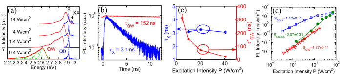
We first compared the optical properties of a large and a small NDs via excitation-intensity-dependent PL study. The large ND is m in diameter and fully strained; it corresponds to the QW-regime and we call it QW-ND. The small ND is 15 nm in diameter and should have the least amount of strain. It was found to be QD-like and will be called QD-ND in this paper.
The emission from the QW-ND is strongly influenced by the strain in the InGaN layer, common to III-N QWs grown on -planeKawakami et al. (2006); Jarjour et al. (2007). At low excitation intensities, as shown in Fig. 1(a), the PL spectra are hundreds of meV broad with pronounced optical-phonon replicas due to the strain-enhanced wavefunction overlapping between electrons, holes and the longitudinal interface optical-phonon modesChen et al. (2007); Renwick et al. (2012). The time-resolved PL (TRPL) decay of the QW-ND is very slow (Fig. 1(b)). In order to quantify the decay time of the QW-ND, we used a mono-exponential function to fit the initial 12.5 ns decay curve and got a initial decay time of ns. Such slow TRPL decay indicates a weak oscillator strength due to large strain-induced electric fields. Note, however, that it is expected that a strained InGaN QW has a stretched exponential decay trace due to the reduction of the carrier density and, thus, the increase of the piezo-electric field over time, which is not obvious in Fig. 1(b) due to the short time window.
With increasing excitation intensity , optical-phonon replicas are reduced, the PL peak energy blueshifts by more than 300 meV (Fig. 1(a)), and the decay time of the emission shortens (Fig. 1(c)) by orders of magnitude. These can all be qualitatively explained by the screening of the built-in field with increased photo-carrier density.
The integrated PL intensity , including optical-phonon replicas, increases super-linearly with the excitation intensity as (Fig. 1(d)). This is because non-radiative recombination processes either have little dependence on carrier density, such as for the Shockley-Hall-Read processShockley and Read (1952), or have negligible contributions over the range of excitation intensities investigated here, such as for the Auger recombinationIveland et al. (2013). Therefore, at higher excitation intensities, an enhanced radiative decay results in an improved IQE, manifested as the super-linear increase of the PL intensity. Assuming that the photo-carrier generation rate is proportional to the excitation intensity , it immediately follows that the IQE increases with as .
In contrast to the QW-ND, the emission from the QD-ND show distinct properties. As shown in Fig. 1(a), at low excitation intensities of W/cm2 the PL of the QD-ND is dominated by a single peak labeled as X at 2.925 eV. The mono-exponential decay time of the X emission ns is much shorter than , suggesting that the built-in electric field is weaker in the QD-ND than in the QW-ND. At high excitation intensities of W/cm2, two additional peaks at higher-energies 2.955 eV (XX) and 2.970 eV (possibly charged XX) appear (Fig. 1(a)). The integrated intensity of the X-peak increases linearly with up to the saturation intensity of W/cm2, while the intensity of the XX-peak increases quadratically with (Fig. 1(d)). Hence we assign peak X to the single exciton emission, and peak XX to the biexciton-to-exciton transition.Seguin et al. (2004); Rice et al. (2005) The large negative binding energies of XX ( meV) are commonly observed in III-N QDsSchömig et al. (2004); Martin et al. (2005); Simeonov et al. (2008); Winkelnkemper et al. (2008); Bardoux et al. (2009); Sebald et al. (2011); Amloy et al. (2012); Chen et al. (2012). It is due to the residual strain, even in dots with such small sizes, which enhances the repulsive exciton-exciton Coulomb interactionSimeonov et al. (2008). Despite the residual strain, both the PL energy (Fig. 1(a)) and decay time (Fig. 1(d)) of the X-peak remain nearly constant as the excitation intensity increases significantly. These again supports that the X-peak comes from the discrete ground state in a zero-dimensional dot, and is thus un-affected by carrier screening. The carrier density only changes the relative occupation among different energy levels, leading to changes in the relative intensities of corresponding spectral lines.
The above study shows that the optical properties of the QW-ND, including PL energy, decay time and IQE, depend strongly on the excitation intensity as a result of strain and screening. On the other hand, in the QD regime, the effect of strain and screening on the exciton emission from the QD-ND becomes obscure due to the energy-level quantization.
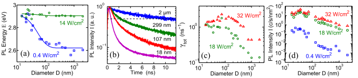
To obtain a quantitative comparison of the effect of strain relaxation on the optical properties of NDs, we performed a controlled systematic study of how PL energy, decay time, and intensity change with the ND diameter. We measured NDs of 21 different diameters, varying from 15 nm – 2 m, fabricated on the same single-QW wafer of fixed thickness ( mono-layer fluctuation) and fixed indium fraction (% fluctuation). For each diameter, we measured one randomly chosen ND from a array for PL energy study (Fig. 2(a)) or all 36 NDs for TRPL and PL intensity studies (Fig. 2(b-d)).
To investigate strain relaxation from the QW to the QD regime, we examined the increase of PL energy with ND diameter reduction as a result of reduced built-in fields as shown in Fig. 2(a). At a high excitation intensity of W/cm2, increases by only meV because of strong photo-carrier screening effects in large NDs. At a low excitation intensity of W/cm2 the photo-carrier screening effect is weak, so that the measured PL energy is closer to the intrinsic exciton transition energy without screening. As decreases from 2 m to 100 nm, increases gradually by meV; with further reduction of from nm to 15 nm, increases rapidly by meV. It shows that the effect of strain-relaxation is most significant for NDs of nm.
The measured relation between PL energy and ND diameter can be described by a compact analytical equationNot :
| (1) |
Here, corresponds to the exciton energy of a fully strain-relaxed InGaN ND, in the limit of nm; corresponds to the energy redshift from in fully strained large InGaN ND, in the limit of , and varies with the excitation intensity ; corresponds to a strain-relaxation length with defines the region from the ND sidewall where strain relaxation is significant. Knowing , and we can also derive a phenomenological exciton potential profile along the ND radiusNot . Fitting the data in Fig. 2(a), where a rapid shift of PL energy was observed for nm, we obtained nm, consistent with earlier numerical predictionsKawakami et al. (2010).
The reduction of strain in smaller NDs corresponds to an increase in the oscillator strength , which should lead to an increase in the radiative decay rate and IQE . However, the excitation efficiency , LDPS and collection efficiency will also change with ND diameter. Taking into account these factors by numerical simulation, we can extract , and from the total decay time and PL intensity.
We obtained the total decay time vs. diameter from the TRPL of ND ensembles. Fig. 2(b) shows TRPL traces of four ensembles. Clearly the decay accelerates as the diameter decreases. All TRPL curves are stretched exponential, as expected for QW-NDs as well as for QD-ND ensembles with inhomogeneous ND properties. We characterized their decay using the half-life-time , the time it takes to go to half of the initial PL amplitudes (dashed line in Fig. 2(b)). Fig. 2(c) shows the total decay rate vs. ND diameter . At both excitation intensities of and W/cm2, the total decay rate (including both radiative and nonradiative decays) increases drastically with the reduction of from m to nm as expected, but plateaus or even slightly decreases with further reduction of . Corresponding to the enhancement in the total decay rate, we measured a drastic increase in , the integrated PL intensity per unit ND area, at a fixed excitation intensity (Fig. 2(d)).
The measured is determined by the excitation intensity , absorption efficiency , IQE and collection efficiency . Therefore, can be calcualted by:
| (2) |
in which , and are averaged , and values over the entire ND and all dipole polarizationsNot . The same definition is used for , , and in the rest of this work.
We evaluate and using the finite-difference-time-domain (FDTD) methodTaflove and Hagness (2005). The results are summarized in Fig. 3(a). The are nearly the same in the QW and QD limits. The highest appears at nm when the GaN nanopillar effectively forms a low-quality cavity in the lateral direction for light at 390 nm wavelengthNot . The first-lens collection efficiency increases from merely 2% in the QW limit to about 30% in the QD limit; and the most drastic increase occurs in the region 40 nm nm. A similar trend in has been predicted for a dipole emitter embedded near the end of a semi-infinite dielectric nanowireFriedler et al. (2009); Bleuse et al. (2011). It was shown thatFriedler et al. (2009), for a large nanopillar, most light is coupled into two guided HE11 modes, one propagating upwards and the other downwards into the substrate. However, the upwards-propagating guided mode is mostly reflected back into the substrate by the top facet of the nanopillar. For a small nanopillarBleuse et al. (2011), the coupling to the guided mode is strongly suppressed while the dissipation into free-space modes is relatively enhanced, leading to an increased collection efficiency.
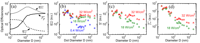
Using Equ. 2 and the calculated and , we extracted as shown in Fig. 3(b). Note that we cannot obtain the absolute value of from Equ. 2, so is a relative value with an arbitrary unit (a.u.). Nonetheless, Fig. 3(b) suggests that the in the QD limit is enhanced compared to that in the QW limit; and the enhancement saturates or even slightly decreases when reduces further. The enhancement is folds at W/cm2, but only % at and 32 W/cm2. This is because at high the oscillator strength in large NDs is already enhanced due to screening. The saturation of at nm in Fig. 3(b) could be due to two factors: the radiative decay rate enhancement is saturated, and at nm the is already close to 100%.
The variation of with can be obtained from as follows:
| (3) |
in which is measured in Fig. 2(c). Fig. 3(c)shows that the improves by only folds as decreases from m to 40 nm and saturates at nm. However, the 10-fold improvement is not the true potential of improvement in our NDs. According to Fermi’s Golden RuleDirac (1927); Novotny and Hecht (2006), is determined by both the oscillator strength and LDPS :
| (4) |
in which, is the ratio of the LDPS of a dipole in a nanopillar to the LDPS of the same dipole in bulk GaN. Note that the oscillator strength , defined as the ratio between the radiative decay rate of the ND in bulk GaN and that of a classical electron oscillator in bulk GaNSiegman (1986), is proportional to the square of the radiative transition matrix elementYu and Cardona (2010). As we shall show below, the in the QD limit is mainly limited by the LDPS factor .
The changes with the change of local dielectric environment. As shown in Fig. 3(a), in the QD limit, the average LDPS factor is strongly suppressed, with . Such a strong suppression in the LDPS should be universal for all nano-emitters closely surrounded by air-dielectric interfaces, such as colloidal QDsMurray et al. (2000), QDs in nanowiresDeshpande et al. (2013); Bounouar et al. (2012); Tatebayashi et al. (2012); Holmes et al. (2013) and QDs at the apices of micro-pyramidsBaier et al. (2004). Experimentally, it has been demonstrated for nano-emitters in nano-spheresSchniepp and Sandoghdar (2002) and nanowiresBleuse et al. (2011). The radiative decay rate in our NDs in the QD limit can be further enhanced by increasing the LDPS. For example, simply by conformal-coating the sample with 150 nm GaN, we can recover the to unity while maintaining the relatively high % in QD-NDsNot . Larger and enhancements may be achieved with more sophisticated structures, such as by enclosing a ND in a micro-cavityGazzano et al. (2013) and in a tapered nanowireClaudon et al. (2010).
With the results of and we can calculate the oscillator strength using Equ. 4. As shown in Fig. 3(d), is enhanced by over 100 folds in the QD limit compared to the QW limit at and 32 W/cm2. The enhancement is a direct result of the strain-relaxation-induced reduction in the piezo-electric polarization fields, which leads to a better overlap between the electron and hole wavefunctions.
In conclusion, we have systematically investigated the optical properties of individual and ensembles of InGaN/GaN nanodisks with precisely controlled diameters varying from the QD limit of less than 40 nm, to the QW limit of up to 2 m. We found significant strain relaxation in nanodisks with diameters less than 100 nm, leading to a 100-fold enhancement in the oscillator strength in the QD limit compared to in the QW limit. Together with the 10-fold suppression in the local density of photon states, this leads to a 10-fold enhancement in the radiative decay rate, which can be further enhanced by increasing the local density of photon states.
We acknowledge financial supports from the National Science Foundation (NSF) under Awards ECCS 0901477 for the work related to materials properties and device design, ECCS 1102127 for carrier dynamics and related time-resolved measurements, and DMR 1120923 (MRSEC) for work related to light-matter interactions. The work related to epitaxial growth, fabrication, and photon antibunching properties were also partially supported by the Defense Advanced Research Project Agency (DARPA) under grant N66001-10-1-4042. Part of the fabrication work was performed in the Lurie Nanofabrication Facility (LNF), which is part of the NSF NNIN network.
References
- Nakamura (1998) S. Nakamura, Science 281, 956 (1998).
- Kako et al. (2006) S. Kako, C. Santori, K. Hoshino, S. Götzinger, Y. Yamamoto, and Y. Arakawa, Nature Materials 5, 887 (2006).
- Deshpande et al. (2013) S. Deshpande, A. Das, and P. Bhattacharya, Applied Physics Letters 102, 161114 (2013).
- Kawakami et al. (2006) Y. Kawakami, S. Suzuki, A. Kaneta, M. Funato, A. Kikuchi, and K. Kishino, Applied Physics Letters 89, 163124 (2006).
- Holmes et al. (2009) M. J. Holmes, Y. S. Park, J. H. Warner, and R. A. Taylor, Applied Physics Letters 95, 181910 (2009).
- Holmes et al. (2011) M. J. Holmes, Y. S. Park, X. Wang, C. C. S. Chan, A. F. Jarjour, R. A. Taylor, J. H. Warner, J. Luo, H. A. R. El-Ella, and R. A. Oliver, Journal of Applied Physics 109, 063515 (2011).
- Hsueh et al. (2005) T. H. Hsueh, H. W. Huang, F. I. Lai, J. K. Sheu, Y. H. Chang, H. C. Kuo, and S. C. Wang, Nanotechnology 16, 448 (2005).
- Chen et al. (2006) H.-S. Chen, D.-M. Yeh, Y.-C. Lu, C.-Y. Chen, C.-F. Huang, T.-Y. Tang, C. C. Yang, C.-S. Wu, and C.-D. Chen, Nanotechnology 17, 1454 (2006).
- Kawakami et al. (2010) Y. Kawakami, A. Kaneta, L. Su, Y. Zhu, K. Okamoto, M. Funato, A. Kikuchi, and K. Kishino, Journal of Applied Physics 107, 023522 (2010).
- Ramesh et al. (2010) V. Ramesh, A. Kikuchi, K. Kishino, M. Funato, and Y. Kawakami, Journal of Applied Physics 107, 114303 (2010).
- Lee et al. (2011) L. K. Lee, L. Zhang, H. Deng, and P.-C. Ku, Applied Physics Letters 99, 263105 (2011).
- Zhang et al. (2013) L. Zhang, C.-H. Teng, T. A. Hill, L.-K. Lee, P.-C. Ku, and H. Deng, Applied Physics Letters 103, 192114 (2013).
- He et al. (2005) Y. He, L. Chen, Y.-K. Song, A. Nurmikko, S.-R. Jeon, Z. Ren, M. Gherasimova, and J. Han, Physica Status Solidi (C) 2, 2740 (2005).
- Purcell (1946) E. Purcell, Physical Review 69 (1946).
- Bleuse et al. (2011) J. Bleuse, J. Claudon, M. Creasey, N. S. Malik, J.-M. Gérard, I. Maksymov, J.-P. Hugonin, and P. Lalanne, Physical Review Letters 106, 103601 (2011).
- Claudon et al. (2010) J. Claudon, J. Bleuse, N. Malik, M. Bazin, P. Jaffrennou, N. Gregersen, C. Sauvan, P. Lalanne, and J. Gérard, Nature Photonics 4, 174 (2010).
- Jarjour et al. (2007) A. Jarjour, R. Oliver, A. Tahraoui, M. Kappers, C. Humphreys, and R. Taylor, Physical Review Letters 99, 1 (2007).
- Chen et al. (2007) D. Chen, Y. Luo, L. Wang, H. Li, G. Xi, Y. Jiang, Z. Hao, C. Sun, and Y. Han, Journal of Applied Physics 101, 053712 (2007).
- Renwick et al. (2012) P. Renwick, H. Tang, J. Bai, and T. Wang, Applied Physics Letters 100, 182105 (2012).
- Shockley and Read (1952) W. Shockley and W. T. Read, Physical Review 87, 835 (1952).
- Iveland et al. (2013) J. Iveland, L. Martinelli, J. Peretti, J. S. Speck, and C. Weisbuch, Physical Review Letters 110, 177406 (2013).
- Seguin et al. (2004) R. Seguin, S. Rodt, A. Strittmatter, L. Reiß mann, T. Bartel, A. Hoffmann, D. Bimberg, E. Hahn, and D. Gerthsen, Applied Physics Letters 84, 4023 (2004).
- Rice et al. (2005) J. H. Rice, J. W. Robinson, J. H. Na, K. H. Lee, R. A. Taylor, D. P. Williams, E. P. O’Reilly, A. D. Andreev, Y. Arakawa, and S. Yasin, Nanotechnology 16, 1477 (2005).
- Schömig et al. (2004) H. Schömig, S. Halm, A. Forchel, G. Bacher, J. Off, and F. Scholz, Physical Review Letters 92, 10 (2004).
- Martin et al. (2005) R. W. Martin, P. R. Edwards, R. A. Taylor, J. H. Rice, J. H. Na, J. W. Robinson, J. D. Smith, C. Liu, and I. M. Watson, Physica Status Solidi (a) 202, 372 (2005).
- Simeonov et al. (2008) D. Simeonov, A. Dussaigne, R. Butté, and N. Grandjean, Physical Review B 77, 075306 (2008).
- Winkelnkemper et al. (2008) M. Winkelnkemper, R. Seguin, S. Rodt, A. Schliwa, L. Reismann, A. Strittmatter, A. Hoffmann, and D. Bimberg, Physica E: Low-dimensional Systems and Nanostructures 40, 2217 (2008).
- Bardoux et al. (2009) R. Bardoux, A. Kaneta, M. Funato, Y. Kawakami, A. Kikuchi, and K. Kishino, Physical Review B 79, 1 (2009).
- Sebald et al. (2011) K. Sebald, J. Kalden, H. Lohmeyer, and J. Gutowski, Physica Status Solidi (B) 248, 1777 (2011).
- Amloy et al. (2012) S. Amloy, E. S. Moskalenko, M. Eriksson, K. F. Karlsson, Y. T. Chen, K. H. Chen, H. C. Hsu, C. L. Hsiao, L. C. Chen, and P. O. Holtz, Applied Physics Letters 101, 061910 (2012).
- Chen et al. (2012) Y. Chen, W. Tsai, W. Chen, and C. Hsiao, Optics Express 20, 2791 (2012).
- (32) See Supplementary Materials in the source package for details of FDTD simulation methods and results for absorption efficiency , local density of photon states factor and first-lens collection efficiency , and a phenomenological understanding of the physical meaning of Equ. 1.
- Taflove and Hagness (2005) A. Taflove and S. Hagness, Computational Electrodynamics: The Finite-Difference Time-Domain Method, The Artech House antenna and propagation library (Artech House, Incorporated, 2005).
- Friedler et al. (2009) I. Friedler, C. Sauvan, J. P. Hugonin, P. Lalanne, J. Claudon, and J. M. Gérard, Optics express 17, 2095 (2009).
- Dirac (1927) P. A. M. Dirac, Proceedings of the Royal Society A: Mathematical, Physical and Engineering Sciences 114, 243 (1927).
- Novotny and Hecht (2006) L. Novotny and B. Hecht, Principles of Nano-Optics (Cambridge University Press, 2006) p. 273.
- Siegman (1986) A. E. Siegman, Lasers (University Science Books, 1986) p. 121.
- Yu and Cardona (2010) P. Yu and M. Cardona, Fundamentals of Semiconductors: Physics and Materials Properties, Graduate Texts in Physics (Springer, 2010) p. 261.
- Murray et al. (2000) C. Murray, C. R. Kagan, and M. G. Bawendi, Annual Review of Materials Science 30, 545 (2000).
- Bounouar et al. (2012) S. Bounouar, M. Elouneg-Jamroz, M. I. Den Hertog, C. Morchutt, E. Bellet-Amalric, R. André, C. Bougerol, Y. Genuist, J.-P. Poizat, S. Tatarenko, K. Kheng, and M. D. Hertog, Nano letters 12, 2977 (2012).
- Tatebayashi et al. (2012) J. Tatebayashi, Y. Ota, S. Ishida, M. Nishioka, S. Iwamoto, and Y. Arakawa, Applied Physics Letters 100, 263101 (2012).
- Holmes et al. (2013) M. Holmes, S. Kako, K. Choi, P. Podemski, M. Arita, and Y. Arakawa, Physical Review Letters 111, 057401 (2013).
- Baier et al. (2004) M. H. Baier, E. Pelucchi, E. Kapon, S. Varoutsis, M. Gallart, I. Robert-Philip, and I. Abram, Applied Physics Letters 84, 648 (2004).
- Schniepp and Sandoghdar (2002) H. Schniepp and V. Sandoghdar, Physical Review Letters 89, 257403 (2002).
- Gazzano et al. (2013) O. Gazzano, S. Michaelis de Vasconcellos, C. Arnold, A. Nowak, E. Galopin, I. Sagnes, L. Lanco, A. Lemaître, and P. Senellart, Nature communications 4, 1425 (2013).