Semiempirical pseudopotential approach for nitride-based nanostructures and ab initio based passivation of free surfaces
Abstract
We present a semiempirical pseudopotential method based on screened atomic pseudopotentials and derived from ab initio calculations. This approach is motivated by the demand for pseudopotentials able to address nanostructures, where ab initio methods are both too costly and insufficiently accurate at the level of the local-density approximation, while mesoscopic effective-mass approaches are inapplicable due to the small size of the structures along, at least, one dimension. In this work we improve the traditional pseudopotential method by a two-step process: First, we invert a set of self-consistently determined screened ab initio potentials in wurtzite GaN for a range of unit cell volumes, thus determining spherically-symmetric and structurally averaged atomic potentials. Second, we adjust the potentials to reproduce observed excitation energies. We find that the adjustment represents a reasonably small perturbation over the potential, so that the ensuing potential still reproduces the original wave functions, while the excitation energies are significantly improved. We furthermore deal with the passivation of the dangling bonds of free surfaces which is relevant for the study of nanowires and colloidal nanoparticles. We present a methodology to derive passivant pseudopotentials from ab initio calculations. We apply our pseudopotential approach to the exploration of the confinement effects on the electronic structure of GaN nanowires.
pacs:
73.21.-b, 78.67.Uh, 78.67.Lt, 31.15.A-, 71.15.DxI Introduction
Much of the computational effort in solving the Kohn-Sham equations of density functional theory (DFT)hohenberg64a ; kohn65a is spent in iteratively updating the screened effective potential. This procedure requires the calculation of the electronic density, obtained over a sum of all occupied Kohn-Sham eigenstates. The required number of states (bands) therefore scales with the number of atoms. For the calculation of optical or transport properties, only the bands close to the band gap are required, which represents, for a large number of atoms, only a small fraction of the total number of bands required for the calculation of the total energy in a self-consistent formalism. An approach that bypasses the calculation of the entire spectrum and focuses on states close to the band gap is the semi-empirical pseudopotential approach.wang95 ; bester09 In this approach the pseudopotential is derived from a DFT calculation in the local density approximation (LDA) and subsequently empirically corrected to reproduce experimental target properties, such as the optical band gap. These semi-emipirical pseudpotentials (SEPs) were derived for CdSe and InP and their accuracy demonstrated.wang95 ; fu97b In this work, we follow a similar procedure for the derivation of nitride SEPs. Former treatment of nitrides were at the level of empirical pseudopotentials (as opposed to SEPs) which assume an empirical analytic functional dependence (a sum of Gaussians) instead of being obtained from DFT-LDA and include only a local component, while the SEPs are angular momentum dependent non-local (or semi-local) potentials.bellaiche96 ; grundmann These empirical pseudopotentials have a parametric strain dependence that is important and more intricate in the case of nitrides than for the case of III-V semiconductors.williamson00 Our derivation of SEPs for nitrides leads to pseudopotentials that are slightly more expensive computationally (they have an angular momentum dependent semi-local component and a slightly larger energy cut-off) but more accurate and transferable. There is no need for an explicit empirical parametric strain dependence. The advantages of SEPs compared to the local empirical pseudopotentials have been discussed earlier, generally to zinc-blende semiconductors.wang95 ; fu97b ; bester09 In this work we have extended the SEP formulation to wurtzite semiconductors, and more specifically to GaN.
The second development that was necessary to properly address nitride nanostructures was the problem of the passivation. In earlier work wang95 ; graf07 the dangling bonds of nanostructures were passivated by empirical Gaussian potentials. The three parameters describing the passivant, namely the width and height of the Gaussian and its distance to the passivating atom, were varied until the surface states, that fill the gaps of most unpassivated semiconductors, disappears. This fitting procedure was originally done manually and subsequently automatized using a minimization procedure.graf07 Even in the case of the exhaustive numerical search of the configuration space, some materials could not be properly passivated. This fact is probably due to the lack of flexibility in the Gaussian function used. In this paper we describe our approach to obtain passivant potentials. It is based on the DFT-LDA calculation of a passivated and an unpassivated (bare) slab. From the difference of both calculations we extract an effective passivant potential in real space. We can accurately fit the numerical results to a Yukawa-type potential.
Once the bulk SEPs for a given material are found, together with its corresponding passivants pseudopotentials, the study of the electronic structure and related properties of nanostructures can be performed. We have chosen as an example to apply the SEP method to GaN nanowires,Goldberger a promising nanostructure in the field of solar cells and optoelectronic devices due to the wide band gap of GaN (3.5 eV), that together with indium nitride, a narrow band gap semiconductor (0.67 eV) can cover the full visible solar spectrum by a proper alloying.wu More specifically, we explore the effects of confinement in the valence and conduction band states close to the nanowire band gap and we discuss the influence of confinement on the optical properties.
II Construction of semiempirical pseudopotentials from bulk LDA calculations
First, we solve the Kohn-Sham equations for the bulk wurtzite structure within the LDA using standard ab initio norm-conserving nonlocal pseudopotentials.gonze09
| (1) |
The Kohn-Sham potential includes the local and nonlocal ionic pseudopotentials and the electron-electron interaction:
| (2) |
The ensuing local part of the self-consistent screened effective potential is defined as:
| (3) |
where is the local part of the non-screened ionic pseudopotential and the term includes the Hartree and exchange-correlation contributions. A more detailed discussion concerning the nonlocal part of the pseudopotential can be found elsewhere.Parr The potential is a periodic function and can be expanded in a Fourier series:
| (4) |
where is the set of the reciprocal lattice vectors of the corresponding crystal structure with unit cell volume .
We now express the periodic potential as a sum over atom-centered potentials :
| (5) |
where we use capital letters for crystal potentials and lower case letters for the corresponding atomic potentials. The vectors are the basis vectors of the crystal unit cell and are the atomic positions of the atoms in the unit cell corresponding to .
The goal now is to obtain an expression for that we could use in other environments, as give for instance in nanostructures. These screened atomic pseudopotentials contain, in addition to the ionic part, in an average way, the contribution related to the electron-electron interaction, expressed by . However, the procedure of obtaining these atomic potentials from the total local potential must be clearly specified and checked for consistency. In the following, we explain how the construction of the screened atomic pseudopotential is carried out.
First, by combining Eqs. (4) and (5), we obtain the following connection between the unknown and the known self-consistent Fourier coefficients , for every value of :
| (6) |
with
| (7) |
where the integral is over the atomic volume , as a consequence of Eq. (5) and after Ref. bester09, . The lattice parameters are taken as Å, and . The wurtzite unit cell has four atoms, with the primitive vectors
| (8) | ||||
and the atom positions of the two anions and two cations
| (9) | ||||
we then obtain for :
| (10) | |||
with the symmetric () and antisymmetric () pseudopotentials
| (11) | |||||
we obtain
| (12) | |||||
Since have inversion symmetry, are real, and they can be written in terms of the real and imaginary parts of
| (13) | |||||
The potential is calculated from the Fourier transform of the LDA crystal potential, . Once are obtained, the reciprocal-space atomic pseudopotentials are obtained from Eq. (11). Through this procedure we can obtain only at discrete values . To palliate this problem the LDA potential of the bulk system is solved for a set of unit cell volumes, at different lattice constants, around the optimized value, as shown below.
So far the procedure to obtain is exact. However, for an efficient implementation it is convenient to assume that the screened pseudopotentials are well represented by their spherically averaged counterparts . At this stage we have a spherically symmetric screened atomic LDA potential .
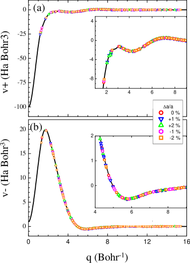
Figures 1(a) and 1(b) show the LDA results (symbols) for and . In order to have a dense grid of points the calculations are performed for five different lattice constants . The data points from different unit cell volumes fall nearly over the same line, with some slight deviations for the data points around Bohr-1 in . This shows that the spherical approximation is justified. Concerning the pseudopotentials at , , their values are arbitrary, and the variation of produces a overall shift of the band structure. The value of is set to the work function, that can be obtained from experimental dataGrabowski2001 or obtained from ab initio calculations. In nanostructures, as superlattices or quantum wells, determines the band alignment and its value has to be set carefully.zhang1993 ; mader In regions of small ( Bohr-1), the changes in the pseudopotentials and do not substantially modify the band structure around the point. In all the cases, we have fitted the data points with cubic splines. In regions of large ( Bohr-1), small oscillations persist, requiring a careful fitting.
In Fig. 2 we plot the corresponding gallium and nitrogen semiempirical pseudopotentials. Concerning the general behavior of the pseudopotentials, the oscillations persist until Bohr-1, which determines the energy cut-off in the subsequent calculations (with a energy cutoff of 30 Ry).
The last step is the solution of the Kohn-Sham equation (1), where the Kohn-Sham potential is replaced by the semiempirical pseudopotentials calculated above, and the nonlocal term . This equation needs to be solved only once, since there is no need to achieve self-consistency.
We proceed by comparing the band structures calculated using the SEP method and the LDA. As the spin-orbit interaction only produces minor splittings in GaN, we have neglected this interaction for the overall band structure comparison, but it will be introduced later on, once the validity of the SEP method has been demonstrated. The effects on the band structures caused by a reduction of the energy cut-off will also be analyzed. In Fig. 3 we plot the following GaN band structures: the LDA results for Ry (black solid lines), the SEP results with Ry, (green dashed lines) and the band gap-corrected SEP results (red dots).
A comparisons of LDA and SEP calculations with the same energy cut-off shows a nearly perfect agreement for all the bands and throughout the Brillouin zone and is not shown. The reduction of the enegy cut-off from 90 Ry to 30 Ry lead to a rigid displacement of the conduction bands towards lower energy, reducing the band gap approximately by 1 eV. The valence band states most affected by the reduction of are those far from the top of the valence band, at around eV. The topmost valence band states remain almost unaltered, and belong to the representation, in agreement with the ab initio band structure. We conclude that the LDA and the SEP band structures are in good agreement for the bands close to the band gap, i.e., the most important part of the band structure in, e.g., photoluminescence experiments.
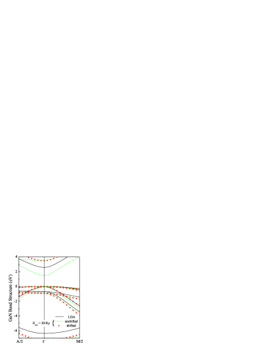
Another important issue in ab initio calculations of semiconductors is the underestimation of the band gap undermining the LDA.bandgap Such underestimation is enhanced, in this special case, if the energy cut-off is reduced. In the SEP-method one can correct this problem easily by multiplying the local potentials by a Gaussian function or renormalizing the nonlocal pseudopotentials.wang95 In this work we have chosen the second possibility where we act on the non-local angular momentum -channel. Figure 3 shows the band structure of the band gap corrected SEPs. The band gap opening does not influence significantly the valence band, although a slight modification is appreciated in the vicinity of the point, which produces a change in the curvature, as expected from the decreased coupling with the valence bands. The conduction band effective mass for the corrected SEPs is now , in good agreement with the reported experimental value of (being the free-electron mass).monemar
For energy cut-offs lower than 30 Ry, the changes in the band structure exceed the admissible margin. The wave functions of the top of the valence band and of the bottom of the conduction band have the same symmetry and shape than the LDA wave functions.
III Surface states and passivation
As noted above, the atoms at the free surfaces of a nanostructure have dangling bonds. The existence of these dangling bonds generates electronic states localized at the surface, with energies usually within the band gap of the semiconductor.wang96a ; franceschetti99 These states can have energies close to the conduction and valence band edges, and can induce an artificial modification of the conduction and valence band states, and they have to be eliminated.puzder03 ; puzder04a ; puzder04b In the literature two methods are used to overcome this difficulty. The first possibility is to achieve quantum confinement by embedding the structure into a virtual material with a high band gap califano03 ; baskoutas11 . The main disadvantage of using this virtual material is the associated increase in the number of atoms. Another way consists of attaching an atom, usually hydrogen, to the dangling bonds (the so-called passivation), which displaces the energies of the surfaces states far from the band gap.xu93 ; huang05 ; reboredo01 However, the determination of the hydrogen pseudopotentials is not a trivial task, and it can depends on the material and of the surface orientation. The simplest way is to model the passivant pseudopotential by an analytical function, such as a Gaussian. The method to optimize the form of the Gaussian function can be a simple trial and error procedure, or a more sophisticated approach, such as a genetic algorithm, as developed in Ref. graf07, . However, the empirical parametrized Gaussian pseudopotentials involve iterative calculations of the electronic structure, which complicates the computational task, and does not always guarantee to achieve an adequate passivation.
In this work, we propose to derive the passivant pseudopotentials from LDA calculations of a small free-standing structure. In the following we describe the necessary steps and illustrate them by an example for the surface of GaN.
Step 1: Ab initio calculation of the self-consistent potential. The self-consistent potential is calculated for two free-standing GaN layers. A bare layer (unsaturated dangling bonds) and a passivated layer (a hydrogen attached to each dangling bond). Specifically, the GaN layer is approximately 15 angstrom thick (24 atoms), and the vacuum layer is about 10 angstrom on both sides to prevent coupling between layers. The input hydrogen norm-conserving potential is taken to be the same for the hydrogen atoms bound to the Gallium and the Nitrogen atom. In the case of materials with metallic surfaces (e.g. CdSe), a satisfactory passivation may require hydrogen potentials with fractional charges. For the atomic positions, we fix the Nitrogen and Gallium atoms to their bulk ideal positions and relax only the distance between the hydrogen atoms (usually two atoms on each side of the slab) and the corresponding passivated atom.distances
The band structures of the bare slab (without geometry optimization) and passivated slab (with optimization of the distance of hydrogen atoms with respect to GaN) are shown in Figs. 4(a) and (b). Note that the bands are rather flat along the direction, which confirms the decoupling between adjacent layers. The energy dispersion along the line of the Brillouin zone is shown, exhibiting the same behavior as in the case of a quantum well.molina09 We observe that conduction and valence bands are very similar in both cases. However, the bare layer has a band gap larger by 0.37 eV. The main difference is obviously the presence of surface states, located within the band gap. These states are grouped in two energy ranges. The states (index assigned in increasing order of energy), are closer to the valence band edge and have a flatter dispersion. The other group, formed by the states and , located in the middle of the band gap, have a more pronounced dispersion. On the contrary, the band structure of the passivated layer has no state within the band gap.
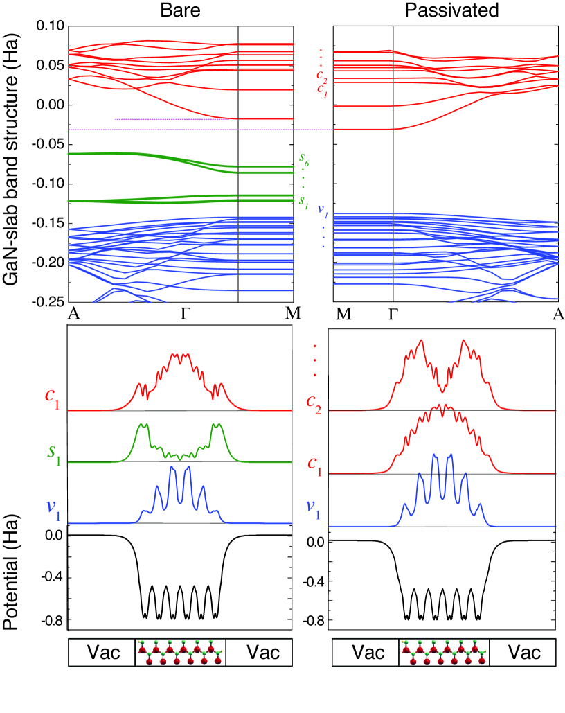
This analysis is further clarified by examining the charge density in real space. Figures 4(c) and (d) show the plane-averaged density corresponding to some relevant states of the bare and passivated -layers, together with the plane-averaged self-consistent potential profile, along the direction. In the case of the bare layer, the mid-gap surface states and present different profiles having a strong hybridization with the layer atoms, penetrating appreciably inside the layer. For the state the penetration into vacuum is significant for both, the passivate and the bare layers, which can be explained by the small electronic effective mass. In the case of the bare layer, the state develops a maximum at the surface of the layer, which is the signature of a hybridization with a surface state. On the other hand, the charge density of the valence band states seems to vanish at the surface without any sign of hybridization, in either the bare or the passivated layer. It is worth to mention that for larger passivated nanostructures the charge density at the border will be negligible. We can also conclude that the dangling bonds affect mainly the states of the conduction band.
Step 2: Determination of the screened hydrogen pseudopotential. We calculate the effective pseudopotential for the atom positions of the unpassivated slab using our semi-empirical pseudopotentials for Ga and N, . We use the same FFT grid as for the self-consistent potential for the passivated slab calculated in the previous step via LDA, . The difference between the two sets of data
| (14) |
represent the modification of the potential in response to the presence of the passivated surface. This includes the effects of the self-consistent charge redistribution around the surface Ga and N atoms, as well as the additional hydrogen potential. The potential is therefore a potential that represents the entire modification of the total potential trough the introduction of a passivated surface. Accordingly, we obtain a different passivant “hydrogen” potential for a Hydrogen atom attached to a Ga atom and for a Hydrogen atom attached to a N atom. To extract a spherically averaged atomic quantity from we calculate the center of potential (akin a center of mass) of a set of points enclosed within a sphere around the hydrogen atomic positions :
| (15) |
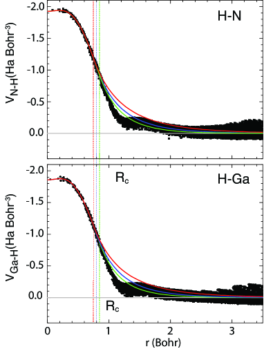
If the potential would be spherical and centered around then and would coincide. In our case, the geometric potential center is slightly shifted from the atomic position and we solve the equation self-consistently until . For the value of we use a value of 1.0 a.u..
Our passivant pseudo-hydrogen pseudopotential is given by
| (16) |
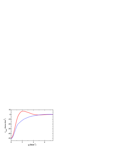
and is shown in Fig. 5, where we plot the discrete set of FFT grid points as black circles. The position of the hydrogen atom has been determined from Eq. (15). The smooth curves in Fig. 5 represent our fits to the data points, where we used three cubic spline functions for . In this region, the data points lie mainly on a curve, which shows that the potential is close to spherically symmetric. For larger radii, the data points show significant scattering along the enegy axis, which is expected, since the potential at the surface will have some non-spherical character. We obtain good results when the data points are fitted by a Yukawa potential:
| (17) |
For the N (Ga) passivant potential we determine = 1.864344 (2.012838) and = 3.7635 (4.060362) with = 0.80 a.u. for a potential in Hartree units.
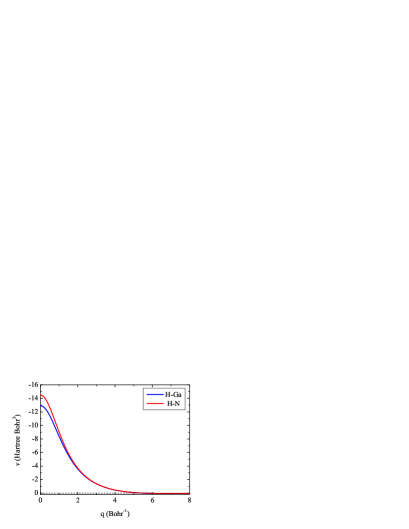
We use a 1D Fourier transformation to obtain the passivant potential in reciprocal space:
| (18) |
with
| (19) |
In Figure 6 we show the pseudo-hydrogen passivant pseudopotentials in reciprocal space for the potential attached to Ga and to N. Both curves are simple and smooth, and deviate from each other only for small values of , i.e. in their long range response, as expected.
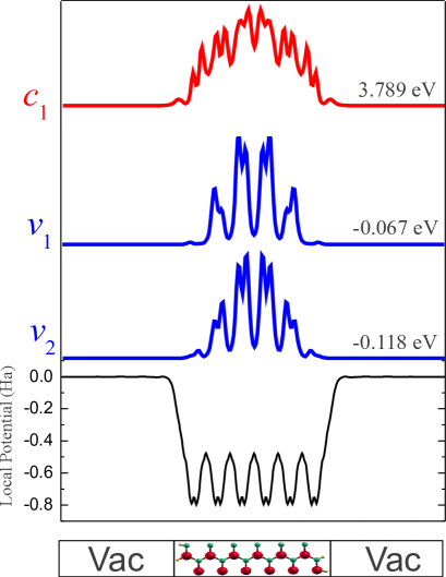
Step 3: Consistency checks on wave functions. The accuracy of the passivation procedure has been checked by applying the SEPM to the same layer used for the LDA calculations. Figure 7 shows the potential and the charge densities of one conduction and two valence band states. The calculation are done with an energy cut-off of 30 Ry and a non-local part of the pseudopotential renormalized to the experimental bulk band gap. All spurious states are removed from the gap and the states are well localized inside the structure. The states and have the same profile than their counterparts LDA states. The small discrepancies can be attributed to the small dimensions of the layer, and gradually disappear for larger nanostructures.website
IV Electronic states of nanowires
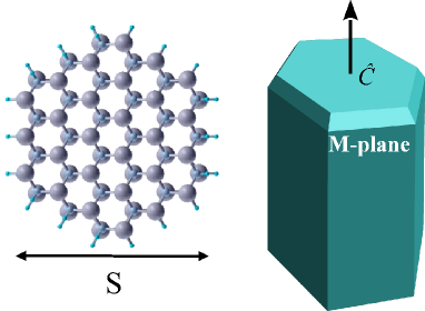
To illustrate the performance of the SEPM in the study of nitride nanostructures, we present here calculations of the electronic structure of free-standing GaN NWs. The NWs are assumed to be oriented along the -axis and infinite in length. We assume a hexagonal cross section, with lateral faces. This is the most usual shape adopted by GaN NWs grown by plasma-assisted molecular beam epitaxy technique.bert1 ; bruno1 This NW faceting has also been supported by theoretical calculations,nort1 showing a lower formation energy for than surfaces. The electronic states are obtained by solving
| (20) |
where the wire potential is constructed as a superposition of atomic pseudopotentials.
In real free-standing NWs a surface reconstruction is expected that would minimizes the total energy of the system. However, in our calculations we will assume for simplicity that the atomic arrangement corresponds everywhere to the perfect wurtzite crystal structure. When building the potential we have passivated the facets using the potential described in section III, which removes states from the gap in all the cases investigated. Equation (20) is solved by imposing artificial periodic boundary conditions on the wire surrounded by layers of vacuum. This transforms Eq. (20) into a Bloch-periodic band-structure problem with a large simulation cell, solved here by expanding in plane waves. We use a sufficiently large wire-wire separation , so that the solutions become independent of . A sketch of the modeled NW is shown in Fig. 8. In the following, the term size refers to the largest lateral dimension, as shown in in Fig. 8 and is labeled as . We have considered a range of sizes from 1.5 to 6.5 nm, which corresponds to a number of atoms varying between 100 to 1500. The matrix diagonalization corresponding to the problem Eq. (20) can be solved using the folded spectrum method.fsm The computational times, within the SEPM, are significantly shorter than they would be in a corresponding self-consistent ab initio calculation.
Here, we will focus on the analysis of the zone center () NW electronic states. These states are naturally classified into valence band (VB, ) and conduction band (CB, ) NW states, and in each case they will be indexed in ascending order, as and , according to their separation in energy from the respective bulk band edges and . Any of the considered states exhibits Kramer’s double degeneracy. When analyzing the corresponding charge densities (here meaning, i.e., the (vertically-averaged) squared wave functions), an envelope pattern is recognized in the cross-section, which corresponds very closely to the radial pattern of the Bessel functions . We find convenient to incorporate this symmetry information to the labeling of the states by adding the notation (meaning: approximately the same symmetry as ), (approximately the same symmetry as ), etc…
In order to further characterize the symmetry of the NW states , we can calculate their projections on the bulk band states, as explained in Ref. baskoutas10, . In particular, in the analysis presented below, we have considered the projections
where are the near-gap () bulk states labeled schematically by their symmetries: (bottom of the CB) and , , .vurgaftman2003
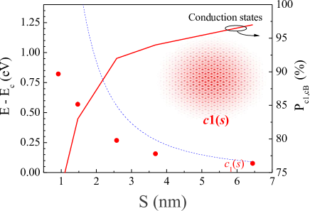
Figure 9 shows the confinement energies (i.e., the energies referred to the bulk CB edge energy) of the CB NW states as a function of the NW size. It is also shows the projection of the lowest energy state onto the CB bulk state , revealing that has between 65 % and 97 % conduction band character. Additionally, the charge density of exhibits a clear -type envelope for all the sizes explored here, in agreement with expectations from the EMA. On the other hand, we have fitted the energy of the state to the function
| (21) |
and have found the values and . The fitted value of the parameter differs significantly from the prediction of the single-band EMA (), which is represented by a dotted line in Fig. 9. We conclude that, even for the case of the almost isolated conduction band, the confinement imposed by the nanowire geometry, while leading to an overall symmetry of the CB states similar to that predicted by the EMA, leads to a remarkably different energy dispersion as a function of NW size.
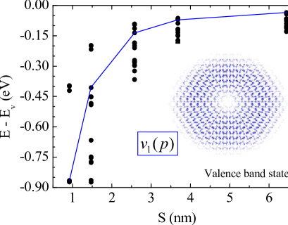
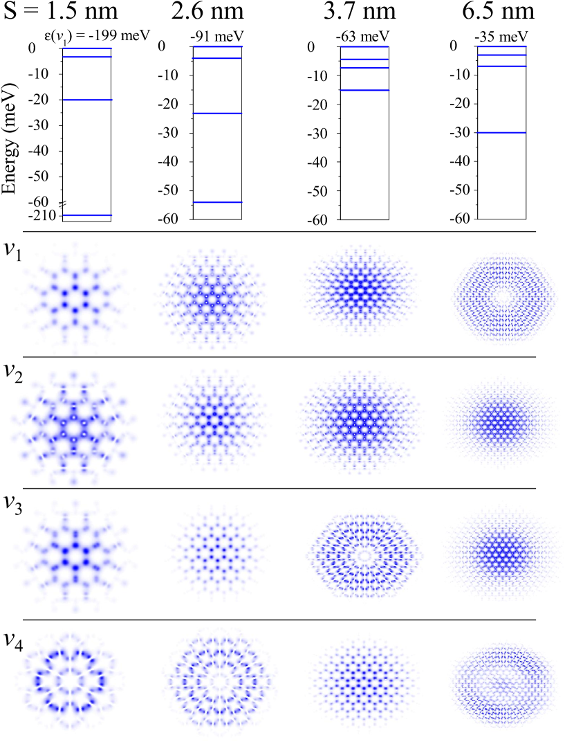
We now turn to the analysis of the VB electronic structure of the NW. Figure 10 shows an overall view of the confinement effects in the VB by displaying the highest energy levels for every NW size. In order to give further insight into the complex evolution of the VB states with sizes, we have represented in Fig. 11 the charge densities of the first four VB states for various NW sizes. A first examination reveals that the wave functions are well confined inside the NWs, and only for some states in the smallest NW show a slight state localization on surface atoms. In particular, the analysis of the charge density of the highest VB state shows that its envelope symmetry changes suddenly from -type for the largest NW to -type for smaller NWs. For the size 2.6 nm and below, the first three VB states show a -type envelope, whereas the VB state with -type envelope is moved to the fourth place in the energy spectrum.
| S(nm) | 1.5 | 2.6 | 3.7 | 6.5 |
|---|---|---|---|---|
| (3, 40, 46) | (76, 8, 6) | (79, 9, 5) | (50, 47, 0) | |
| (60, 7, 5) | (7, 68, 17) | (9, 75, 11) | (82, 12, 3) | |
| (4, 29, 53) | (3, 8, 85) | (48, 45, 1) | (18, 76, 3) | |
| (41, 42, 0) | (45, 45, 0) | (3, 6, 89) | (38, 42, 16) |
The above study must be complemented with the analysis of the projections of the NW VB states onto the bulk states , and , at the point, which will give us additional information about the symmetry of the states. In Table. 1 we have summarized the values of the corresponding projections (, and ), for the same set of states as in Fig. 11. For the largest nanowire shown here, the composition of the topmost state, which has envelope symmetry, is almost equally divided between the bulk states and . The next two VB states, and , of -symmetry, clearly show a dominant contribution from bulk bands () and (), respectively. Neither of these states has a significant contribution from the -band. When the nanowire size is reduced to 3.7 nm, we observe that the two highest VB states have now dominant contributions from - and -bands, with symmetry, whereas the mixed - state becomes now the third state, . If one further reduces the NW size to 2.6 nm and below, the mixed - state now becomes , whereas the first three states show a high degree of -- mixing. Thus, our detailed analysis of the NW wave functions as a function of size has allowed us to identify a state with -type envelope symmetry which is essentially an equal-weight mixture of bulk bands and . In Fig. 10 we have traced a line connecting these states. The change in the symmetry of the highest VB state as a function of size is just one of the consequences of the nontrivial interplay between symmetry mixing, spin-orbit coupling and confinement effects on the NW valence band electronic structure. This is in contrast to the simpler situation of the CB electronic structure. This unconventional trend of the nanowire electronic structure has also been reported by calculations using the tight-binding method.Persson2008 ; molina2012 Moreover, studies in other wurtzite systems, as the one made in ZnO nanocrystals by S. Baskoutas and G. Bester baskoutas10 shows also that the highest state of the valence band is characterized by a -type envelope.
V Conclusion
We have followed the idea wang95 ; fu97b to use the screened effective potential from a DFT bulk calculation to extract a spherically averaged atomic pseudopotential. We have derived the analytic connection between the screened DFT effective potential and the atomic quantities in the case of wurtzite bulk unit cells. This allowed us to derive atomic semi-empirical pseudopotentials for nitride materials. The pseudopotentials are non-local, in the same way as DFT norm-conserving pseudopotentials, and reproduce the DFT results for the eigenvalues of bulk up to a few meV. Our potentials are not aimed at the calculation of total energies but at the calculations of the eigenvalues and eigenfunctions around the band gap, which gives some leverage on the reduction of the energy cut-off, compared to DFT calculations. The advantage of the method compared to the original empirical pseudopotential approach (see Ref. Cohen70, and references therein) resides in the direct link to ab-intio calculations and the ensuing rather simple fitting procedure of a curve through a dense set of data points. The transferability of the potentials are good for the situations studied here but are expected to degrade when charge transfer significantly deviates from the bulk situation. This represents a general limitation of the method that we, however, palliate for the case of a free surface by deriving effective passivant potentials (see next paragraph). The defective band gap inherited from DFT is correct by a slight adjustment of the non-local channel of the potential which has only a very marginal effect on the wave functions, as shown previously wang95 ; fu97b ; li05a . The derived method should be applicable to other materials. Eventually, the method can be built on the basis of GW calculations. However, full self-consistent GW calculations are still prohibitive in the applications to extended systems and only work for small molecules.rinke12
In the second part of this work, we have established a simple and direct methodology to obtain the passivating pseudo-hydrogen pseudopotentials, essential for the treatment of free surfaces in nanowires or nanoparticles. We thereby use the difference between the screened effective DFT potentials of a passivated structure and the semiempirical pseudopotential of the corresponding unpassivated structure. The derivation is done in real space and we find that a cubic spline interpolation up to a cut-off radius , connected to a Yukawa potential leads to satisfactory results.
The suitability of the semi-empirical pseudopotential method and of our passivation procedure has been explored in GaN nanowires. Due to the high confinement of NW sizes below 10 nm, the use of accurate atomic potentials is unavoidable, as continuous methods are expected to fail in the description of such systems. We have found that, while the conduction band states follow a behavior compatible with the EMA predictions, the valence band states exhibit a complex evolution as a function of the NW size. We find drastic variations in the character of the wave functions with the NW size, which will influence optical properties such as the polarization of the photoluminescence.
VI Acknowledgements
A. Molina-Sánchez thanks the Deutscher Akademischer Austausch Dienst (DAAD) for funding the research stay at the Max-Planck Institute für Festkörperforschung in Stuttgart (Germany), and the group of Gabriel Bester for its kind hospitality.
References
- (1) P. Hohenber and W. Kohn, Phys. Rev. 136, B864 (1964).
- (2) W. Kohn and L. J. Sham, Phys. Rev. 140, A1133 (1965).
- (3) L.-W. Wang and A. Zunger, Phys. Rev. B 51, 17398 (1995).
- (4) G. Bester, J. Phys. Condens. Mat. 21, 023202 (2009)
- (5) H. Fu and A. Zunger, Phys. Rev. B 55, 1642 (1997).
- (6) L. Bellaiche, S.-H. Wei, and Z. Zunger, Phys. Rev. B, 54, 17568 (1996).
- (7) D. Fritsch, H. Schmidt, and M. Grundmann, Phys. Rev. B 67, 235205 (2003).
- (8) A. J. Williamson, L.-W. Wang, and A. Zunger, Phys. Rev. B 62, 12963 (2000).
- (9) P. A. Graf, K. Kim, W. B. Jones, and L.-W. Wang, J. Comp. Phys. 224, 824 (2007).
- (10) J. Goldberger, R. He, Y. Zhang, S. Lee, H. Yan, H.-J. Choi, and P. Yang. Nature 422, 599 (2003).
- (11) J. Wu. J. Appl. Phys. 106, 011101 (2009).
- (12) All DFT calculations are done with ABINIT. X. Gonze, B. Amadon, P.-M. Anglade, J.-M. Beuken, F. Bottin, P. Boulanger, F. Bruneval, D. Caliste, R. Caracas, M. Cote, T. Deutsch, L. Genovese, Ph. Ghosez, M. Giantomassi, S. Goedecker, D.R. Hamann, P. Hermet, F. Jollet, G. Jomard, S. Leroux, M. Mancini, S. Mazevet, M.J.T. Oliveira, G. Onida, Y. Pouillon, T. Rangel, G.-M. Rignanese, D. Sangalli, R. Shaltaf, M. Torrent, M.J. Verstraete, G. Zerah, J.W. Zwanziger, Computer Phys. Commun. 180, 2582 (2009).
- (13) R. G. Parr and W. Yang, Density-Functional Theory of Atoms and Molecules, (Oxford University Press, 1989).
- (14) S. P. Grabowski, M. Schneider, H. Nienhaus, W. Monch, R. Dimitrov, O. Ambacher, and M. Stutzmann. Appl. Phys. Lett. 78, 2503 (2001).
- (15) S. Zhang, C. Yeh, A. Zunger, Phys. Rev. B, 48, 11204 (1993).
- (16) K. Mader and A. Zunger, Phys. Rev. B, 50, 17393 (1994).
- (17) L. J. Sham and M. Schlüter, Phys. Rev. Lett. 51, 1888 (1983).
- (18) B. Monemar, J. Phys: Condens. Matt. 13 7011 (2001).
- (19) L.-W. Wang and A. Zunger, Phys. Rev. B 53, 9579 (1996).
- (20) A. Franceschetti, H. Fu, L.-W. Wang, and A. Zunger, Phys. Rev. B 60, 1819 (1999).
- (21) A. Puzder, A. J. Williamson, F. A. Reboredo, and G. Galli, Phys. Rev. Lett. 91, 157405 (2003).
- (22) A. Puzder, A. J. Williamson, F. Gygi, and G. Galli, Phys. Rev. Lett. 92, 217401 (2004).
- (23) A. Puzder, A. J. Williamson, N. Zaitseva, G. Galli, L. Manna, and A. P. Alivisatos, Nano Lett. 4, 2361 (2004).
- (24) M. Califano, G. Bester, and A. Zunger, Nano Lett. 3, 1197 (2003).
- (25) S. Baskoutas and G. Bester, J. Phys. Chem. C 115, 15862 (2011).
- (26) Y. N. Xu and W. Y. Ching, Phys. Rev. B 48, 4335 (1993).
- (27) X. Huang, E. Lindgren, and J. R. Chelikovsky, Phys. Rev. B 71, 165328 (2005).
- (28) F. A. Reboredo and A. Zunger, Phys. Rev. B 63, 235314 (2001).
- (29) The distances are and , in units of GaN bulk distance, .
- (30) A. Molina, A. García-Cristóbal, and A. Cantarero, Microelectr. J. 40, 418 (2009).
- (31) All the pseudopotentials can be found, tabulated, at the following website: http://www.fkf.mpg.de/bester/ and in the suplementary material.
- (32) K. A. Bertness, A. Roshko, L. M. Mansfield, T. E. Harvey, and N. A. Sanford, J. Cryst. Growth 300, 94 (2007).
- (33) R. Songmuang, O. Landré, and B. Daudin, Appl. Phys. Lett. 91, 251902 (2007).
- (34) J. E. Northrup and J. Neugebauer, Phys. Rev. B 53, R10477 (1996).
- (35) L.-W. Wang and Z. A., J. Chem. Phys. 100, 2394 (1994).
- (36) S. Baskoutas and G. Bester, J. Phys. Chem. C 114, 9301 (2010).
- (37) I. Vurgaftman and J. R. Meyer, J. Appl. Phys. 94, 3675 (2003).
- (38) M. P. Persson and A. Di Carlo, J. Appl. Phys. 104, 073718 (2008).
- (39) A. Molina-Sánchez and A. García-Cristóbal, J. Phys.: Condens. Matter 24, 295301 (2012).
- (40) M. L. Cohen and V. Heine. The fitting of pseudopotentials to experimental data and their subsequent application. Vol. 24 of Solid State Physics pp. 37-248 (Academic Press, 1970).
- (41) J. Li and L.-W. Wang, Phys. Rev. B 72, 125325 (2005).
- (42) F. Caruso, P. Rinke, X. Ren, M. Scheffler, and A. Rubio, Phys. Rev. B 86, 081102(R) (2012).