Ferroelectric and dielectric characterization studies on relaxor- and ferroelectric-like strontium-barium niobates
Abstract
Ferroelectric domain structure evolution induced by an external electric field was investigated by means of nematic liquid crystal (NLC) method in two strontium-barium niobate single crystals of nominal composition: Sr0.70Ba0.30Nb2O6 (SBN:70 — relaxor) and Sr0.26Ba0.74Nb2O6 (SBN:26 — ferroelectric). Our results provide evidence that the broad phase transition and frequency dispersion that are exhibited in SBN:70 crystal have a strong link to the configuration of ferroelectric microdomains. The large leakage current revealed in SBN:26 may compensate internal charges acting as pinning centers for domain walls, which gives rise to a less restricted domain growth similar to that observed in classical ferroelectrics. Microscale studies of a switching process in conjunction with electrical measurements allowed us to establish a relationship between local properties of the domain dynamics and macroscopic response i.e., polarization hysteresis loop and dielectric properties.
Key words: relaxor ferroelectrics, niobates, domain walls, switching process, SBN
PACS: 77.80.Dj, 77.80.Fm, 77.80.Jk, 77.84.Dy, 77.22.Ej
Abstract
Еволюцiя сегнетоелектричної доменної структури, iндукованої зовнiшнiм електричним полем дослiджувалась за допомогою методу нематичного рiдкого кристалу в двох монокристалах стронцiй-барiєвого нiобату номiнального складу: Sr0.70Ba0.30Nb2O6 (SBN:70 — релаксорний) i Sr0.26Ba0.74Nb2O6 (SBN:26 — сегнетоелектричний). Нашi результати показують, що широкий фазовий перехiд i частотна дисперсiя, продемонстрованi кристалом SBN:70, мають тiсний зв’язок iз конфiгурацiєю сегнетоелектричних мiкродоменiв. Великий струм стiкання, виявлений в SBN:26, може компенсувати внутрiшнi заряди, що дiють як центри пiнiнгу для доменних стiнок, що приводить до менш обмеженого росту доменiв подiбно до того, що спостерiгається в класичних сегнетоелектриках. Мiкромасштiбнi дослiдження процесу перемикання в поєднаннi з електричними вимiрюваннями дозволяють встановити спiввiдношення мiж локальними властивостями динамiки доменiв i макроскопiчним вiдгуком, а саме, гiстерезисною петлею поляризацiї i дiелектричними властивостями.
Ключовi слова: релаксорний сегнетоелектрик, нiобати, доменнi стiнки, процес перемикання, SBN
1 Introduction
Strontium-barium niobates, SBN (SrxBa1-xNb2O6, ), are ferroelectric crystals that have received a great interest in their applications in optoelectronics [1]. The controlled manipulation of the domain structure via external electric field involves an important issue of potential applications, such as optical-frequency conversion and high density optical data storage [2]. Thus, efforts are directed towards producing SBN crystals with high quality ferroelectric domain reversible structures. Polarization switching, which proceeds by nucleation and growth of domains, has attracted much attention also from the viewpoint of statistical physics related to solid-state transformation.
Only a few works focusing on SBN domain structure dynamics can be found in literature. Mostly, high-resolution domain structure studies (nanoscale domains) have been performed for a congruently melting composition Sr0.61Ba0.39Nb2O6 (SBN:61) by piezoresponse force microscopy (PFM) [3, 4, 5, 6, 7, 8]. The microscale domain structure kinetics in SBN:61 was investigated using an electro-optic imaging microscope [9, 10] and NLC method [11, 12, 13]. The observed specific features of the switching process were accounted for freezing or pinning domain walls connected with disordered structure of SBN crystals.
SBN has an open tetragonal tungsten bronze structure, in which only five of six available positions of Sr2+ and Ba2+ cations are occupied [14]. The origin of relaxor behaviour in SBN can be attributed to the development of a quenched random fields associated with the composition/structural disorder [15, 16]. The ferroelectric properties of SBN system change with the composition [17, 18]. To the best of our knowledge, there is no report on the domain structure dynamics in other SBN compositions, in spite of its significant effect on the physical properties. Temperature dependence of dielectric permittivity , at various frequencies has shown a gradual crossover from typical relaxor behaviour in SBN:75 into classical ferroelectrics as observed in the case of SBN:40 [18, 19]. It is reflected by a broad peak of function, which was strongly dependent on frequency for SBN:75 crystal; while a sharper peak, with the position of the maximum of function independent of frequency, was observed for SBN:40.
In this report, we have used the NLC method to study the domain creation process in static electric fields, in SBN:70 and SBN:26 compositions. The NLC method involves the averaging over macroscopic scale and this enables us to correlate the domain structure dynamics with macroscopic characterization techniques such as electric displacement – electric field () hysteresis loop, switching currents and dielectric permittivity measurements. Investigating the change from relaxor (SBN:70) to classical ferroelectric behaviour (SBN:26) is thus helpful for better understanding the physics of the relaxor ferroelectrics.
2 Experimental details
SBN crystals, as uniaxial ferroelectric materials, exhibit only 180∘ domains because the paraelectric phase has a tetragonal symmetry (4/mmm), and the order parameter in the ferroelectric phase (4mm) occurs along [001] direction [14]. Details concerning the crystal fabrication by Czochralski method are given elsewhere [18]. Two large single crystals of nominal composition Sr0.70Ba0.30Nb2O6 (SBN:70) and Sr0.26Ba0.74Nb2O6 (SBN:26) have been grown. Using an Inductively Coupled Plasma – Optical Emission Spectroscopy (ICP–OES), a real composition of the grown single crystals was determined to be Sr0.70Ba0.26Nb2O5.96 and Sr0.35Ba0.69Nb2O6.04, respectively. The obtained single crystals seem to be slightly non-stoichiometric. Despite an obvious difference between the nominal and real compositions, the samples are labelled throughout the paper by their nominal stoichiometry. Platelet-shaped samples were cut perpendicular to the [001] direction and polished to the optical quality.
The NLC mixture of p-methoxybenzylidene-p-n-butylaniline (MBBA) and pethoxybenzylidene-p-n-butylaniline (EBBA) was used to observe optically indistinguishable 180∘ domain walls. The NLC method makes possible a continuous observation of the domain pattern during polarization reversal in an electric field if a cover glass coated with a conducting layer of tin oxide is used. The reversed regions, where reorientation of domains still occurs, look somewhat darker than the ‘‘grey’’ surrounding domains, because a certain electrohydrodynamic instability, particularly dynamic scattering, takes place in these regions [20]. The () hysteresis loops were recorded using a modified Sawyer-Tower circuit by using an field of frequency 50 Hz and a digital oscilloscope. Switching current transients were measured using a wave-form function generator, a small standard resistor and digital oscilloscope. The complex linear susceptibility was measured using a Solartron 1260 Impedance Analyzer together with a 1296 Dielectric Interface (SBN70) and an Agilent E4980A Precision LCR Meter (SBN26) applying a weak probing electric field of the order of 2 Vcm-1. For electric and dielectric studies, the SBN samples were prepared as plates with dimensions mm3 with Cu-Au electrodes evaporated onto the principal (001) faces. Thin copper interface is to improve the adhesion of gold. The temperature protocols required by experiment were managed using a Lake Shore Model 340 temperature controller.
3 Experimental results
3.1 Ferroelectric characteristics
Figure 1 presents the temperature dependences of real parts of electric susceptibility of SBN:70 and SBN:26 measured at different frequencies. The SBN:70 displays a typical relaxor behavior where the temperature position of the broad maximum of susceptibility and its height strongly depend on the frequency of the driving electric field. On the other hand, SBN:26 shows much higher susceptibility peaks () taking place at a fixed temperature, K. These maxima might be considered as a sign of a phase transition between an ordered ferroelectric and paraelectric states. Since the electric conductivity (leakage current) of SBN:26 increases distinctly at higher temperatures, the measurements of susceptibility were carried out only at higher frequencies of the probing field ( and Hz). Under this condition the effect of the leakage current on the dielectric response may be neglected.
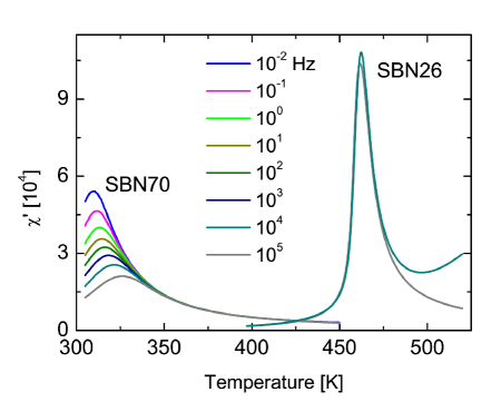
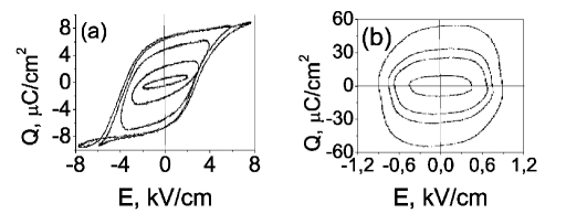
Figure 2 shows the room temperature loops for SBN:70 (a) and SBN:26 (b) compositions. These loops were obtained by applying a sinusoidal signal at a frequency of 50 Hz. The polarization charges accumulated on the crystal sample result from various effects of the crystal bulk, such as changes in the domain structure and leakage currents. The loops of the SBN:26 sample, present an oval-like profile owing to the large leakage current in the crystal sample. It is difficult to determine the coercive field, which increases steadily with an increase of the electric field amplitude. These results suggest that even at high electric fields, there are frozen regions that do not participate in the switching polarization and/or that a large contribution to the polarization is due to the sidewise domain wall motion, which is a very slow mechanism.
3.2 Domain switching in SBN:70 crystal
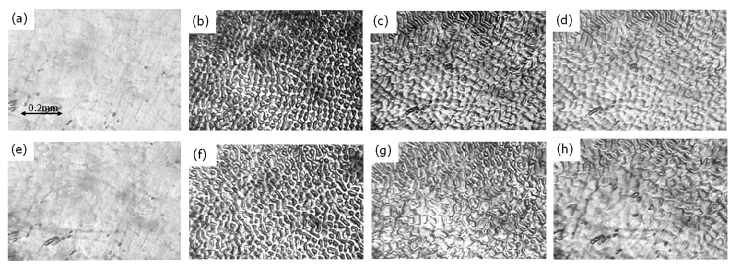
To investigate the domain dynamics, the crystal sample was preliminary poled into a single domain state with a sufficiently high electric field , and then an electric field of the opposite direction was applied to the sample. The formation of domains is possible if the amplitude of field exceeds some threshold value at a given site of the crystal, which depends on the state of the aging of the sample. The static domain structure gave no contrast. Figure 3 illustrates the domain pattern evolution observed in SBN:70 crystal sample at room temperature when external electric field is switched on. The dark areas correspond to the areas which actually reversed their polarization direction while clear areas are the regions where the switching process has not started [initial polarization state in figure 3 (a)] or has already been completed. The switching process is realized by the nucleation and growth of domains. We use the term ‘‘nucleation’’ to describe the emergence of new antiparallel domains within the original domain as they appear in the video image. However, it is an open question whether the initial domain state is single-domain or contains the nano-scale residual domains not resolved by the NLC method. It should be emphasized that the thickness of the visible ‘‘wall’’ is not a real physical thickness of the domain wall, which is much smaller (of the order of several unit cells). The sidewise movement of the domain walls in SBN:70 crystals is strongly perturbed by the random field environment related to the relaxor properties and to the resulting domain wall pinning effect [15, 16]. Local structure disorder gives rise to quenched random fields whose fluctuations are the source of local enhancements of the coercivity. As a result of the pinning effect, some wall segments change their position from image to image, whereas others stay immobile for a long time. As a consequence, a maze type domain pattern is formed. A close inspection revealed that individual domain walls expand with a great resistance under the field and finally clamp the entire dynamics. The pronounced slowing down of the domain walls is reflected in a poor contrast of NLC above the slowly moving domain walls, as can be seen in figure 3 (d) and more clearly in figure 3 (e), where domain walls are hardly seen. The variations of the domain pattern are noticeable following the application of the higher electric field of 1.3 kV/cm. Simultaneously, a fine domain structure appears, as can be seen in figure 3 (f). With pinning centres present in the crystal, large domains are broken up into smaller ones since certain areas of the domains are incapable of switching, and consequently this process is accompanied by an increase of the domain density. However, the polarization is fully reversed in the observed surface area after a further poling in kV/cm. The switching process is completed first in the central part of the image in figure 3 (h) (where no obvious domain walls can be identified), then in the outer region of the video scan. This field is also sufficient to reverse the polarization state in the entire volume of the examined SBN:70 crystal sample.
The fast polarization switching process was investigated by measuring the switching currents in response to square wave electric pulses. A set of square pulses (of 10 ms duration) was applied by combining two positive and two negative pulses in series. A true switching current was then obtained by subtracting the nonswitching current from the switching one. Figure 4 presents the switching curves obtained for various amplitudes of the electric fields for SBN:70 crystal sample. The rate of polarization switching at constant can be found from the switching current by integration of from to the instant . The results are presented in figure 4. The observed ‘‘partial’’ saturation of polarization may confirm the fact that there are slowly switching regions that do not contribute to the switching current signals even in . This should be related to the ‘‘pinning effect’’ of the domain walls in SBN:70 crystal sample. The values of polarization obtained by the pulsed field technique are comparable to that obtained from hysteresis-loop (H-L) measurements at the same pulse amplitude of the -field at frequency 50 Hz. The maximum value of polarization /cm2 found by H-L at frequency Hz and kVcm-1 is small compared to the total polarization of about 20 /cm2 obtained from the measurements at a very low-frequency of in which all domains can be aligned [21, 22]. It was found from pyroelectric measurements that a total polarization of a polydomain crystal requires the field exposure times that can range up to several tens of seconds even for the fields well above the coercive field [21]. In contrast to the stable H-L measured at high frequency of -field, a non-coincidence of trajectories of H-L was obtained during quasistatic loop registration in the course of a repeated field cycling [21, 22]. This process was accompanied by a considerable decrease in the amplitude of polarization (the so-called fatigue effect).
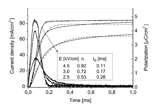
The relaxation of polarization is well described by a Kohlrausch, Williams and Watts (KWW) stretched exponential function with widely used in dielectric relaxation studies. The fits are represented by broken lines in figure 4. The KWW function is usually used to describe a complex relaxation and can reflect a very broad distribution of relaxation times [23, 24]. This is closely related to a distribution of random electric fields inherent to relaxor crystals. It is interesting to note that KWW function described the switching kinetics in SBN:61 [13] as well as the relaxing domains on the nanoscale, with PFM imaging of the domain configuration in SBN:61 doped with cerium [5].
3.3 Domain switching in SBN:26
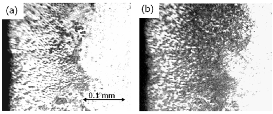
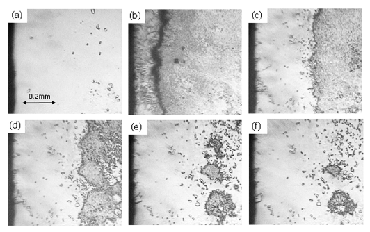
Microscopic observations of the domain pattern show that SBN:26 crystals usually contain intrinsic defects in concentration high enough to effect the rate of domain nucleation and growth in certain regions of the crystal sample. As is shown in figure 5, the distribution of nucleation sites is not random. Such spatially non-uniform distribution of domain nuclei suggests the presence of a frozen polarization component or built-in field, which favours one direction of spontaneous polarization in certain regions. The fact that a similar picture of delineated domains has been observed for a positive [figure 5 (a)] and a negative [figure 5 (b)] polarization state, demonstrates the presence of a frozen polarization state, possibly due to locally accumulated defects. The symmetry of the hysteresis loop for SBN:26 crystal sample also indicates a lack of built-in directional field, which could stabilize the domain structure in a preferential direction. We observed a very slight variation in the domain size during the switching process in low electric fields due to the domain wall pinning effect. When the external field exceeds some threshold value (1 kV/cm for the crystal sample examined), the domain walls begin to move from the crystal edge, as is shown in figure 6. The evolution of the domain pattern takes place via expansion of the domain front formed after coalescence of newly created domains at the edge of the crystal sample [figures 6 (b)–(d)]. After a sufficient waiting time ( s) along with the progress in switching, the macroscopically visible domains arise in the area before the moving domain front (in the region where nucleation process is suppressed). The new domains are clearly seen in figure 6 (d). The domain wall front mobility is strongly inhomogeneous over the crystal surface. A marked slowing down of the domain wall velocities was observed during its propagation. Very approximate estimations give values from m/s at the initial stage to m/s at the end of the switching process in kV/cm. At higher electric fields, the nucleated domains have been observed almost on the whole crystal surface, and the switching speed increases.
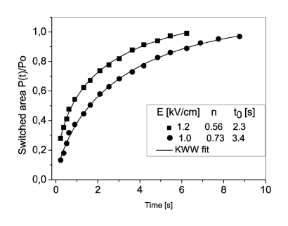
The pulse switching technique for studying the switching behaviour in higher electric fields for SBN:26 crystals is inappropriate because the conduction current obscures the displacement current. Kinetics of polarization relaxation was determined in low electric fields by measuring the fraction of the switched area as a function of time since the domain structure is naturally linked to the polarization state of the crystal. Optical microscopy inspection on the opposite polar faces showed a nearly complete penetration of the domains throughout the crystal bulk. It means that the forward domain growth along the polarization direction takes place very quickly, and the sidewise domain growth determines the kinetics of polarization switching. Thus, the domain growth becomes a two-dimensional problem. Therefore, the area of the switched domains normalized to the total scan area is expected to be close to the normalized reverse polarization. The recording of the domain patterns was performed with a digital camera. In order to obtain a quantitative description of the polarization evolution, the data have been processed using an image analysis program. Figure 7 exemplarily illustrates the evolution of the switched areas as a function of time under two different applied fields. The data points are well fitted (solid lines) with KWW function, where the values of the stretching exponent, , are given in figure 7.
4 Discussion
It is interesting to note that the domain switching process in SBN:70 single crystals is similar to that observed in Ni doped SNB:61 single crystals [13]. It was shown that Ni doping additionally deteriorates the homogeneity of the SBN:61 crystals. In both type of crystals, only the electric field is sufficient to complete the microscale domain switching in the entire volume of the crystal sample. In the doped SBN:61 and SBN:70 single crystals, slow and fast domain walls coexist, which could play an important role in the ferroelectric phase transition broadening, assuming the formation of polar regions with locally different Curie temperature. On the other hand, the domain switching in SBN:26 crystal in the high-field regime may qualitatively resemble the switching observed in classical ferroelectric crystals, in which the growth of the existing domains is more favourable than the creation of new ones due to a relatively low domain-wall energy [25]. Thus, the nucleated domains expand with no or little resistance under an electric field. The SBN:26 crystal exhibits a high electrical conductivity. There has been reported a considerable increase of the leakage current density since the applied field exceeds a critical value in SBN crystals with low Sr content [17, 26]. Once the domains are nucleated in the high-field regime, the field induced charge carriers may compensate the sources of random fields giving rise to the depinning of the domain walls in SBN:26 crystals. It has been reported that having raised the sample conductivity by illumination, the pinning centres were eliminated and the polarization dynamics was fully restored in doped SBN:61 crystals [27].
The relaxation of polarization during the switching process can be described in the examined single crystals by KWW stretched exponential function. It is interesting to note that our results are consistent with a general concept saying that dynamical heterogeneity was established as a possible source of a stretched exponential relaxation [23].
The domain walls make a considerable contribution to the total dielectric response of the SBN system investigated. One can presume that a weak measuring field in dielectric measurements does not affect the domain configuration but creates nuclei on the domain walls. Our results may confirm that the composition disorder could play an important role in the dielectric response in SBN:70. A broad distribution of the heights of local pinning barriers should yield a distribution of activation energies for the nucleation of reversed steps on the existing domain walls. Consequently, SBN:70 crystals show much broader temperature dependence and lower values of dielectric susceptibility than those observed in SBN:26 crystals, in which the motion of domain walls is less restricted by a random field environment. Dielectric measurements as well as the domain switching observations have evidenced the change from typical relaxor behaviour in SBN:70 into classic ferroelectric behaviour in the case of SBN:26 crystal. It is interesting to note that the crossover from relaxor to ferroelectric behaviour was also observed in solid solutions of BaTi1-xSnxO3, and was evidenced by dielectric spectroscopic data [28].
It must be noted that visualization of the domain structure by NLC method may not thoroughly reflect the domain structure evolution in electrical switching at the same pulse amplitudes. Due to a slow response time (of the order of several ms), liquid crystal molecules may not follow the changes of the domain structure in the regions that exhibit high speed switching. Moreover, the results of the works show a strong effect of an interface (electrode and ferroelectric surface) conductivity on the kinetics of the switching process [29]. In a metal contact, electrical charges can freely move and can effectively screen the depolarization field accompanying the ferroelectric polarization, which decreases the switching process. However, visualization of a domain structure by NLC-method can be used in checking the quality of the crystal for the purpose of choosing high quality SBN samples with a homogeneous distribution of domain nuclei.
5 Conclusions
The NLC decoration technique is a relatively simple method to visualize the distribution and evolution of the microscale domains during the switching process, which obviously reflects the internal disorder of a crystal. The domain structure dynamics confirm the dielectric measurements stating that the ferroelectric properties of SBN system change with the composition from strong relaxor behaviour in SBN:70 into classical ferroelectrics as observed in the case of SBN:26. Characteristic features of the domain structure dynamics in SBN crystal of different composition (SBN:70 and SBN:26) can serve as a direct verification of the concept of local random fields that exist due to a structural disorder of the SBN crystal. Fluctuations of random fields neither effect the entire domains nor form a macroscopic bias field, but act as pinning centres for the domain walls in SBN:70 crystal. For SBN:26 crystal, the domain walls can only be pinned in low electric fields. At higher fields, the field- induced charge carriers may compensate the sources of random fields giving rise to a less restricted domain growth. The polarization switching process in both crystals can be described by a stretched exponential function widely used in dielectric relaxation studies.
Acknowledgements
Thanks are due to the Polish Ministry of Science for a partial financial support under grant No. N N507 455034. Professor W. Kleemann from the University of Duisburg-Essen is acknowledged for making accessible the Solartron Impedance Analyzer.
References
- [1] Ramirez M.O., Molina P., Bausá L.E., Opt. Mater., 2012, 34, 524; doi:10.1016/j.optmat.2011.03.016.
- [2] Soergel E., Appl. Phys. B, 2005, 81, 729; doi: 10.1007/s00340-005-1989-9.
-
[3]
Shur V.Ya., Shikhova V.A., Pelegov D.V., Ievlev A.V., Ivleva L.
I., Phys. Solid State, 2011, 53, 2311;
doi:10.1134/S106378341111028X. - [4] Terabe K., Takekawa S., Nakamura M., Kitamura K., Higuchi S., Gotoh Y., Gruverman A., Appl. Phys. Lett., 2002, 81, 2044; doi:10.1063/1.1506945.
- [5] Lehnen P., Kleemann W., Woike Th., Pankrath R., Phys. Rev. B, 2001, 64, 224109; doi:10.1103/PhysRevB.64.224109.
-
[6]
Shvartsman V.V., Kleemann W., Łukasiewicz T.,
Dec J., Phys. Rev. B, 2008, 77, 054105;
doi:10.1103/PhysRevB.77.054105. -
[7]
Liu X.Y., Liu Y.M., Takekawa S., Kitamura K., Ohuchi F.S.,
Li J.Y., J. Appl. Phys., 2009, 106, 124106;
doi:10.1063/1.3273481. - [8] Gainutdinov R.V., Volk T.R., Lysova O.A., Razgonov I.I., Tolstikhina A.L., Ivleva L.I., Appl. Phys. B, 2009, 95, 505; doi:10.1007/s00340-009-3507-y.
- [9] Tian L., Scrymgeour D.A., Gopalan V., J. Appl. Phys., 2005, 97, 114111; doi:10.1063/1.1925330.
- [10] Shur V.Ya., Pelegov D.V., Shikhova V.A., Kuznetsov D.K., Nikolaeva E.V., Rumyantsev E.L., Yakutova O.V., Granzow T., Ferroelectrics, 2008, 374, 33; doi:10.1080/00150190802424785.
-
[11]
Ivanov N.R., Volk T.R., Ivleva L.I., Chumakova S.P.,
Ginsberg A.V., Cryst. Rep., 2002, 47, 1023;
doi:10.1134/1.1523521. -
[12]
Matyjasek K., Wolska K., Kaczmarek S.M.,
Rogowski R.Z., J. Phys.: Condens. Matter, 2008, 20, 295218;
doi:10.1088/0953-8984/20/29/295218. -
[13]
Matyjasek K., Wolska K., Kaczmarek S.M., Subocz J.,
Ivleva L.I., Appl. Phys. B, 2012, 106, 143;
doi:10.1007/s00340-011-4773-z. - [14] Jamieson P.B., Abrahams S.C., Bernstein J.L., J. Chem. Phys., 1968, 48, 5048; doi:10.1063/1.1668176.
- [15] Nattermann T., Shapir Y., Vilfan I., Phys.Rev. B, 1990, 42, 8577; doi:DOI:10.1103/PhysRevB.42.8577.
- [16] Kleemann W., Phase Trans., 1998, 65, 141; doi:10.1080/01411599808209285.
- [17] Qu Y.Q., Li A.D., Shao Q.Y., Tang Y.F., Wu D., Mak C.L., Wong K.H., Ming N.B., Mater. Res. Bulletin, 2002, 37, 503; doi:10.1016/S0025-5408(02)00676-1.
-
[18]
Łukasiewicz T., Swirkowicz M.A., Dec J., Hofman W.,
Szymski W.J., J. Cryst. Growth, 2008, 310, 1464;
doi:10.1016/j.jcrysgro.2007.11.233. -
[19]
Santos I.A., Mendes R.G., Eiras J.A., de Los J., Guerra S.,
Araújo E.B., Appl. Phys. A, 2009, 95, 757;
doi:10.1007/s00339-008-5060-7. - [20] Tikhomirova N.A., Dontsova L.J., Pikin S.A., Shuvalov L.A., JETP Lett., 1979, 29, 34.
- [21] Granzow T., Doerfler U., Woike Th., Woehlecke M., Pankrath R., Imlau M., Kleemann W., Phys. Rev. B, 2001, 63, 174101; doi:10.1103/PhysRevB.63.174101.
-
[22]
Gladkii V.V., Kirikov V.A., Volk T.R., Isakov D.V.,
Ivanova E.S., Phys. Solid State, 2003, 45, 2171;
doi:10.1134/1.1626758. - [23] Chamberlin R.V., Phase Transit., 1998, 65, 169; doi:10.1080/01411599808209287.
-
[24]
Rogowski R.Z., Matyjasek K., Wolska K., Kaczmarek S.M.,
Phase Transit., 2008, 81, 1039;
doi:10.1080/01411590802457946. - [25] Miller R.C., Weinreich G., Phys. Rev., 1960, 117, 1460; doi:10.1103/PhysRev.117.1460.
-
[26]
Matyjasek K., Repow K., Kaczmarek S.M., Berkowski M., J. Phys.: Condens. Matter, 2007, 19, 466207;
doi:10.1088/0953-8984/19/46/466207. - [27] Granzow T., Doerfler U., Woike T., Woehlecke M., Pankrath R., Imlau M., Kleemann W., Europhys. Lett., 2002, 57, 597; doi:10.1209/epl/i2002-00503-6.
-
[28]
Shvartsman V.V., Dec J., Xu Z.K., Banys J., Keburis P.,
Kleemann W., Phase Transit., 2008, 81, 1013;
doi:10.1080/01411590802457888. - [29] Shur V.Ya., J. Mater. Sci., 2006, 41, 199; doi:10.1007/s10853-005-6065-7.
Ukrainian \adddialect\l@ukrainian0 \l@ukrainian
Сегнетоелектричнi i дiелектричнi дослiдження стронцiй-барiєвих нiобатiв релаксорного i сегнетоелектричного типу
К. Матиясек, Я. Дец , С. Мiґа, Т. Лукасєвiч
Iнститут фiзики, факультет механiчної iнженерiї i
мехатронiки,
Захiдно-померанський технологiчний унiверситет, Щецiн, Польща
Iнститут матерiалознавства, Сiлезький унiверситет,
Катовiце, Польща
Iнститут технологiї матерiалiв електронiки, Варшава, Польща