Influence of bulk inversion asymmetry on the magneto-optical spectrum of a HgTe topological insulator
Abstract
The influence of bulk inversion asymmetry in and grown HgTe quantum wells is investigated theoretically. The bulk inversion asymmetry leads to an anti-crossing gap between two zero-mode Landau levels in a HgTe topological insulator, i.e., the quantum well with inverted band structure. It is found that this is the main contribution to the anti-crossing splitting observed in recent experimental magneto spectroscopic measurements. The relevant optical transitions involve different subbands, but the electron-electron interaction induced depolarization shift is found to be negligibly small. It is also found that the splitting of this anti-crossing only depends weakly on the tilting angle when the magnetic field is tilted away from the perpendicular direction to the quantum well. Thus, the strength of bulk inversion asymmetry can be determined via a direct comparison between the theoretical calculated one-electron energy levels and experimentally observed anti-crossing energy gap.
pacs:
73.21.Fg, 73.22.Dj, 73.61.Ga, 78.66.HfI Introduction
In recent years, topological insulators have attracted considerable attentions for their exotic electronic properties.Zhang08Phys ; Hasan10RevModPhys ; Moore10Nature For a HgTe quantum well, when the well width exceeding a critical value, the system will become a two-dimensional topological insulator and this theoretical prediction has been confirmed experimentally.Zhang06 ; Konig07Science ; Konig08
An effective four-band modelZhang06 ; Konig07Science ; Konig08 is proposed to describe the two-dimensional topological insulator made of a HgTe quantum well grown along the direction, and many interesting aspects have been explored based on this model system.Niu08 ; Liu08PRL ; Schmidt09PRB ; Li09PRL ; Novik10PRB ; Lindner11naturephys ; Chang11PRL
The effective model predicts that, when a perpendicular magnetic field is applied to the quantum well with inverted band structure, two zero-mode Landau levels will cross each other and become degenerate at a critical magnetic field. The degeneracy can be lifted and an anti-crossing gap can appear when one includes the effect of bulk inversion asymmetry existing in the HgTe quantum well in constructing the effective model. The edge states originated from these two zero Landau levels have different dependence on its cyclotron center coordinate. The energy of electron-like state will bend upward, and the hole-like state will bend downward. Below and above the critical magnetic field, these two zero Landau levels exchanges order in energy. The above features of two zero Landau levels are the key to the explanation of experimentally observed field driven insulator-metal-insulator transition.Konig07Science ; Konig08
When there is an anti-crossing gap opening at the critical magnetic field, the edge states will be a mixture of electron-like and hole-like states, it would be interesting to know its dependence on the cyclotron center coordinate, e.g., the possibility of a non-monotonic edge states dispersion. This clearly demands a more detailed and careful study of the nature of gap opening. In a tight binding theoretical calculation, the size of splitting at the critical magnetic field between two zero Landau levels due to bulk inversion asymmetry has been estimated.Konig07Science More recently, experimental investigations are reported where magneto spectroscopic measurements are performed on HgTe quantum well samples which are grown not only in but also in directions.mag2011 ; mag2012 An anti-crossing of the resonance modes versus the magnetic field is observed and the bulk inversion asymmetry is proposed as one of the possible origins.mag2011 ; mag2012
In this paper, the influence of bulk inversion asymmetry in a HgTe quantum well is studied within an eight-band approach. The strength of bulk inversion asymmetry enters as a parameter to be determined. It is found that the bulk inversion asymmetry leads to an anti-crossing gap between two zero Landau levels as expected. The relevant optical transitions observed experimentally involve different subbands, therefore we have to examine the electron-electron interaction induced depolarization shift which is known to be important in low-dimensional quantum structures.Ando82RMP ; kotthaus ; tung It is found that, in both and grown HgTe quantum wells, the depolarization shift is negligibly small. We also study the effect due to the tilting of the applied magnetic field. It is found that the anti-crossing gap only depends weakly on the tilting angle. The depolarization shift remains negligible for small tilting angle. Thus, the strength of bulk inversion asymmetry can be determined via a direct comparison between the theoretical calculated one-electron energy levels and experimentally observed anti-crossing energy gap, without invoking a more complicated theory. This can also provide a realistic parameter for the effective four-band model when one uses it in the presence of an externally applied magnetic field.
This paper is organized as follows: In section II, the theoretical formulation is briefly presented. Section III contains our calculated results and their discussions. Finally, in the last section, a summary is provided.
II Formulation and calculation
The calculation of one-electron energy levels is based on the well documented eight-band approach.winkler For details about this method, e.g., the operator ordering, the inclusion of a magnetic field, the influence of remote bands, the influence of strain, and the modification due to heterojunction interfaces, we refer to a partial list of publications and references therein.bahder ; burt ; foreman ; smith ; zawadzki ; rossler In our calculation, the influence of strain is included and is found to be important quantitatively. The quantum well is assumed to be parallel to the plane, and the external magnetic field is along the direction when it is not tilted. The valence band of the HgTe quantum well is taken as the zero energy point. The parameter for the bulk inversion asymmetry is denoted as instead of in order to avoid possible confusion.bahder In our calculation, the axial approximation is not used.mag2011 ; mag2012 The influence of bulk inversion asymmetry in a HgTe quantum well is also discussed in Ref.ssc for the zero magnetic field case.
Calculations are carried out for symmetric and asymmetric HgTe quantum wells with HgxCd1-xTe as barriers. Results shown are mainly for symmetric quantum wells with barriers. The asymmetrical quantum well studied has a step well structure consisting of a HgxCd1-xTe barrier, a HgyCd1-yTe well, a HgTe well, and a HgxCd1-xTe barrier. The band parameters used in our calculation are taken from a recent magneto spectroscopy study.mag2012 The bulk inversion asymmetry parameter , whose value is not known, is taken as an adjustable parameter in order to see its effect.
After obtaining electronic energy levels, different transition energies can be easily calculated. In order to make a clear comparison with the experiment, one should know the nature of the transition. This is achieved by calculating the corresponding optical transition matrix elements between two involved states.ziman ; yu Assuming the two states are denoted as and , we will calculate , and . Two matrix elements and give the same information. In the calculation of above matrix elements, one should take into account the contribution from the Bloch basis states,yang ; liu as the intersubband optical transition is not fundamentally different from the inter-band optical transition. In previous studies,yang ; liu the optical transition matrix element is calculated for the case of zero magnetic field. In the following, is shown in the unit of eV with the free electron mass in vacuum.
The depolarization field correction is due to the electron-electron interaction in the quantum well. This effect can be taken into account via a self-consistent linear response approach. It can cause a shift to the transition energy and a splitting between two degenerated transitions.Ando82RMP ; kotthaus ; tung When the transition involves two states and , one may have a non-zero dynamical polarization charge density
This charge density generates a dynamical electric field in the direction perpendicular to the quantum well. The corresponding potential should be taken into account self-consistently. When one has transitions from occupied states to empty states, the relevant matrix element is given by with the dielectric constant of HgTe, the magnetic field strength, and the quantum well width. The dimensionless is defined as
where denotes the transition between and , denotes the transition between and . The matrix element gives the shift of transition energy, and with gives the coupling between two transitions which may lead to a splitting between degenerated transitions.Ando82RMP ; kotthaus ; tung
III Results and discussions
In Fig.1, the energy levels of a HgTe quantum well grown in the direction are shown as a function of the quantum well width . The in-plane wave vector is zero. There is no externally applied magnetic field, and a symmetrical quantum well is assumed.
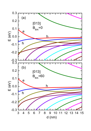
In Fig.1(a), , and in Fig.1(b), eVÅ2. Similar to the case of a grown HgTe quantum well, one observes that when nm, the energy of electron-like state (marked by the symbol e) becomes lower than the energy of hole-like state (marked by the symbol h). One has the so-called inverted band structure.Zhang06 Our calculation indicates that the critical well width for a quantum well is slightly smaller than that of a quantum well of the same structure.
In the case of grown quantum well, our calculation indicates that the critical quantum well width is almost not affected by the introduction of a non-zero . For a grown quantum well, a non-zero leads to an obvious gap opening at the critical quantum well width. The energies of lower subbands are also affected. In contrast, no obvious gap opening can be seen for a grown quantum well, when becomes non-zero. This difference between quantum wells grown in different directions is due to the symmetry change. Because of the emerging of band energy order inversion, the grown HgTe quantum well should also be a topological insulator similar to the grown HgTe quantum well.Zhang06
In Fig.2, energy levels are shown versus the strength of a perpendicular magnetic field for (a) a HgTe quantum well grown in the direction, and (b) grown in the direction. eVÅ2. The quantum well width is nm. It is clear that an energy gap is opened between two zero Landau levels as marked by circles. From Fig.2(a) and Fig.2(b), one observes that the critical magnetic fields is nearly the same for and grown quantum wells. In Fig.2, various transitions are labelled as , , …, and , with dashed-line-arrows indicating the initial and final states involved. In the case of grown quantum well, one of the zero Landau level merges with higher Landau levels at a non-zero magnetic field and this is marked by an arrow in Fig.2(b).
Our calculation indicates that, when the or grown quantum well is not symmetric about the center of the quantum well (a step well structure with ), no obvious gap opening can be seen when . When eVÅ2, it is found that, in the asymmetrical quantum well, the gap between two zero Landau levels is not obviously changed compared to the corresponding symmetrical quantum well. In the reported experiments,mag2011 ; mag2012 the two zero Landau levels are fully occupied, and one expects that the exchange effect due to electron-electron interaction may shift their energy.Ando82RMP However, we believe that the influence of this exchange effect on the size of gap, due to non-zero , between two zero Landau levels is small, because the wave functions of these two zero Landau levels have similar -dependence and similar components of Landau levels.
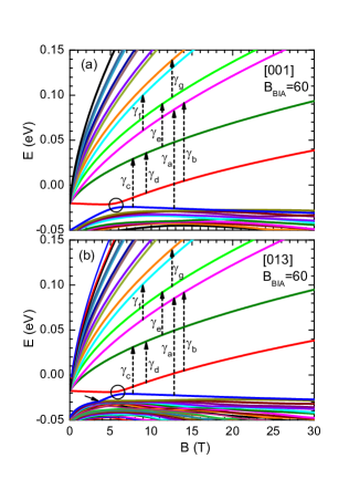
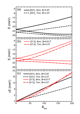
Next, let us examine the transition energy and corresponding optical transition matrix elements. In Fig.3(a), the energies of various transitions are shown versus the magnetic field. In Fig.3(b) and Fig.3(c), the corresponding optical transition matrix elements versus the magnetic field are displayed.
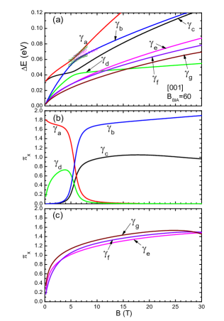
The calculation is done for a HgTe quantum well grown in the direction. These transitions are selected because they are relevant to the experiments.mag2011 ; mag2012 The quantum well is a symmetric one and the quantum well width is nm. eVÅ2. The magnetic field is perpendicular to the quantum well. Symbols in Fig.3(a) are experimental data and this will be discussed later.
At low magnetic fields, transitions , , and should be observable, but they become invisible at high magnetic fields as the initial states involved are depopulated. The strength of these transitions is shown in Fig.3(c). They show similar magnetic field dependence and have similar magnitude as well.
As the magnetic field increases, transitions and should become observable as the final states become available for these transitions. Around the critical magnetic field (see also the circle marks in Fig.2), the transition strength shows a clear anti-crossing behavior as shown in Fig.3(b). This is consistent with the experimental observation.mag2011 Transitions and have lower transition energies. They also display an anti-crossing behavior but with relatively weaker transition strength. In an experiment, transitions and may not be observable if the final states involved are fully occupied. They should become observable at higher magnetic fields.
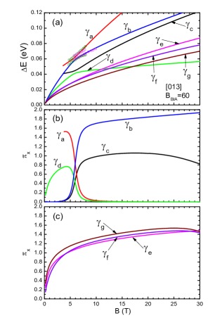
We also perform calculation of the optical transition properties for a HgTe quantum well grown in the direction in the presence of a perpendicular magnetic field. The results are shown in Fig.4. The quantum well is a symmetric one, and the quantum well width is nm. eVÅ2. In Fig.4(a), the energies of various transitions versus the magnetic field are shown. Symbols in Fig.4(a) are experimental data. In Fig.4(b) and Fig.4(c), the corresponding optical transition matrix elements are displayed. One sees that the magnetic field dependence of transition energies and of optical transition matrix elements are qualitatively the same as that of a grown quantum well. This is consistent with the nm HgTe quantum well experimental results reported.mag2011 ; mag2012
In Fig.5, the energy levels are shown as a function of , the strength of bulk inversion asymmetry, at fixed magnetic fields and fixed quantum well widths.
In Fig.5(a), the result is for the grown HgTe quantum wells, and Fig.5(b) is for the grown quantum wells. The quantum wells are assumed to be symmetrical ones. In both and grown quantum wells, the critical magnetic field becomes smaller for narrower quantum wells. As increases, the energy of one state increases, while the energy of the other state decreases. The gap between these two zero Landau levels increases as increases. This is shown in Fig.5(c). For the grown quantum well, the gap size increases faster for the well of wider well width. For the grown quantum well, the gap size evolves almost in the same way for the two wells with different well width. The gap size for the nm grown quantum well can be smaller or larger than the gap size of of the nm grown quantum well. The gap size reported in the magneto spectroscopy experiments is about to meVmag2011 ; mag2012 . Our calculation is consistent with the experiments.
Our calculation indicates that the value of critical magnetic field shown in Fig.2 and Fig.3 is sensitive to the strain parameters. In our calculation, the strain is treated in the so-called coherent interface approximation for both and grown quantum wells, and the reconstruction of interface is not considered.decao Different treatment of the strain effect may produce different quantitative results. However, this requires a careful microscopic structure study of the interface between quantum well and barrier and this is beyond the scope of the present paper.
Next, we study the effect of a tilted magnetic field. In a III-V compound semiconductor quantum well, the tilting of magnetic field away from the perpendicular direction to the quantum well is used to couple Landau levels and subbands or to tune the ratio between the cyclotron resonance energy and Zeeman spin splitting. It is a useful experimental tool.Ando82RMP ; tung
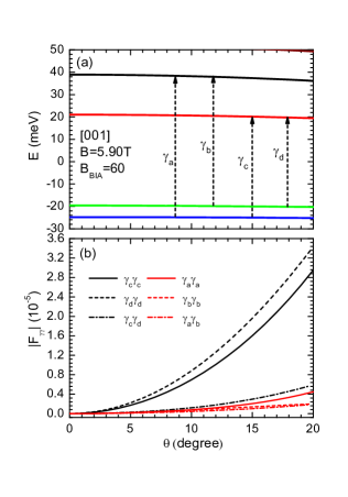
In Fig.6(a), the energies of two zero Landau levels (two lower ones) and energies of two higher Landau levels are shown versus the tilting angle . The concerned transitions are labelled in the same way as in Fig.2. The calculation is done for a grown HgTe quantum well of width nm. The fixed magnetic field is Telsa, and eVÅ2. The quantum well is a symmetrical one. One observes that two higher Landau levels show a small decrease in energy as the tilting angle increases. The energies of the two zero Landau levels are almost independent of tilting angle studied.
In Fig.6(b), the depolarization field correction matrix element is shown for various transitions versus the tilting angle. The off diagonal term involving different transitions is very small. It is found that at , the depolarization effect can be safely ignored. As the tilting angle increases, the matrix elements for and transitions increase more rapidly than that of other transitions. However, for small tilting angles shown in the figure (less that degree), the correction due to the depolarization effect remain negligible. The depolarization correction matrix element is proportional to with a factor meV for HgTe. Thus, the correction is of the order meV. This value is too small to explain the experimental findings.
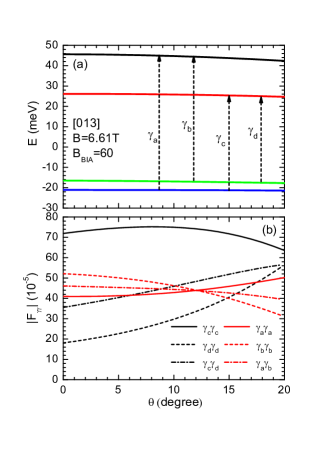
In Fig.7(a), the energy levels of concerned transitions are shown versus the tilting angle for a grown HgTe quantum well. The quantum well is symmetric and well width is nm. eVÅ2. One sees that the tilting angle dependence of energy levels shown in Fig.7(a) is similar to that shown in Fig.6(a). In Fig.7(b), the depolarization field correction matrix element is shown versus the tilting angle. However, different from that of a grown quantum well, at , the matrix elements for all transitions become obviously non-zero, and are much larger than that shown in Fig.6(b) (see the vertical scale of Fig.7(b)). This is due to the lowering of symmetry in the grown quantum well. However, as the magnitude of remains small, for small tilting angles, the correction due to the depolarization effect is about meV, still too small to account for the experimental observations.
We have also investigated the tilting angle dependence for step-well asymmetric quantum wells with and . It is found that, the tilting angle dependence of energy levels and depolarization corrections is nearly the same as that shown in Fig.6 and Fig.7. The tilting angle dependence of concerned transition energies is small, and the depolarization correction is negligible. Now, we can compare our calculated results in Fig.5(c) with the experiments,mag2011 ; mag2012 we estimate that should take a value about to eVÅ2. In Fig.3(a) and Fig.4(a), experimental data near the anti-crossing region are extracted from Refs.mag2011 ; mag2012 and are displayed. The open circles are from Ref.mag2011 , and open squares are from Ref.mag2012 . It is clear that, the agreement is reasonably good.
IV Summary
In summary, the influence of bulk inversion asymmetry in and grown HgTe/HgxCd1-xTe quantum wells is studied theoretically. The dependence of electronic states on the quantum well width, the magnitude of externally applied magnetic field, and the tilting angle of the magnetic field is examined. Our study suggests that a grown HgTe/HgxCd1-xTe quantum well is also a topological insulator when the quantum well width exceeding a critical value about nm. The bulk inversion asymmetry leads to an anti-crossing gap between two zero-mode Landau levels and is the main contribution of this splitting. The electron-electron interaction induced depolarization shift is found to be negligibly small. The splitting due to the bulk inversion asymmetry only weakly depends on the tilting angle when the magnetic field is tilted. Thus, the strength of bulk inversion asymmetry can be determined via a direct comparison between the theoretical calculated one-electron energy levels and the experimentally observed anti-crossing splitting.
Acknowledgements.
This work was partly supported NSF of China via projects 61076092 and 61290303.References
- (1) S. C. Zhang, Physics, 1, 6 (2008); X. L. Qi and S. C. Zhang, Physics Today, 63, 33 (2010).
- (2) M. Z. Hasan and C. L. Kane, Rev. Mod. Phys. 82, 3045 (2010).
- (3) J. E. Moore, Nature, 464, 194 (2010).
- (4) B. A. Bernevig, T. L. Hughes, and S. C. Zhang, Science. 314, 1757 (2006).
- (5) M. König, S. Wiedmann, C. Brüne, A. Roth, H. Buhmann, L. W. Molenkamp, X. L. Qi, and S. C. Zhang, Science, 318, 766 (2007).
- (6) M. König, H. Buhmann, L. W. Molenkamp, T. Hughes, C. X. Liu, X. L. Qi, and S. C. Zhang, J. Phys. Soc. Jpn. 77, 031007 (2008).
- (7) B. Zhou, H. Z. Lu, R. L. Chu, S. Q. Shen, and Q. Niu, Phys. Rev. Lett. 101, 246807 (2008).
- (8) C. X. Liu, T. L. Hughes, X. L. Qi, K. Wang, and S. C. Zhang, Phys. Rev. Lett. 100, 236601 (2008).
- (9) M. J. Schmidt, E. G. Novik, M. Kindermann, and B. Trauzettel, Phys. Rev. B, 79, 241306 (2009).
- (10) J. Li, R. L Chu, J. K. Jain, and S. Q. Shen, Phys. Rev. Lett. 102, 136806 (2009).
- (11) E. G. Novik, P. Recher, E. M. Hankiewicz, and B. Trauzettel, Phys. Rev. B, 81, 241303 (2010).
- (12) N. H. Lindner, G. Refael, and V. Galitski, Nature Physics, 7, 490 (2011).
- (13) K. Chang and W. K. Lou, Phys. Rev. Lett. 106, 206802 (2011).
- (14) M. Orlita, K. Masztalerz, C. Faugeras, M. Potemski, E.G. Novik, C. Brüne, H. Buhmann, and L.W. Molenkamp, Phys. Rev. B 83, 115307 (2011).
- (15) M. Zholudev, F. Teppe, M. Orlita, C. Consejo, J. Torres, N. Dyakonova, M. Czapkiewicz, J. Wróbel, G. Grabecki, N. Mikhailov, S. Dvoretskii, A. Ikonnikov, K. Spirin, V. Aleshkin, V. Gavrilenko, and W. Knap, Phys. Rev. B 86, 205420 (2012).
- (16) T. Ando, A. B. Fowler and F. Stern, Rev. Mod. Phys. 54, 437 (1982).
- (17) R. J. Warburton, C. Gauer, A. Wixforth, J. P. Kotthaus, B. Brar, and H. Kroemer, Phys. Rev. B 53, 7903 (1996).
- (18) L. C. Tung, X. G. Wu, L. N. Pfeiffer, K. W. West, and Y. J. Wang, J. Appl. Phys. 108, 083502 (2010).
- (19) R. Winkler, Spin-Orbit Coupling Effects in Two-Dimensional Electron and Hole Systems (Springer, Berlin, 2003).
- (20) T. B. Bahder, Phys. Rev. B 41, 11992 (1990); T. B. Bahder, Phys. Rev. B 46, E9913 (1992).
- (21) M. G. Burt, J. Phys. Condens. Matter 4, 6651 (1992).
- (22) B. A. Foreman, Phys. Rev. B48, 4964 (1993).
- (23) D. L. Smith and C. Mailhiot, Rev. Mod. Phys. 62, 173 (1990).
- (24) P. Pfeffer and W. Zawadzki, Phys. Rev. B 41, 1561 (1990); P. Pfeffer and W. Zawadzki, Phys. Rev. B 53, 12813 (1996).
- (25) H. Mayer and U. Rössler, Phys. Rev. B 44, 9048 (1991).
- (26) R. Winkler, L. Y. Wang, Y.H. Lin, and C. S. Chu, Solid State Commun. 152, 2096 (2012).
- (27) J. M. Ziman, Principles of the Theory of Solids (Cambridge University Press, Cambridge, 1972).
- (28) P. Y. Yu and M. Cardona, Fundamentals of Semiconductors Physics and Materials Properties (Springer, Berlin, 2001).
- (29) R. Q. Yang, J. M. Xu, and M. Sweeny, Phys. Rev. B 50, 7474 (1994).
- (30) H. C. Liu, M. Buchanan, and Z. R. Wasilewski, Appl. Phys. Lett. 72, 1682 (1998).
- (31) L. De Caro and L. Tapfer, Phys. Rev. B 51, 4374 (1995).