Efficiency of electrical manipulation on two-dimensional topological insulators
Abstract
We investigate the efficiency of electrical manipulation on two-dimensional topological insulators by considering a lateral potential superlattice on the system. The electronic states under various conditions are examined carefully. It is found that the dispersion of the mini-band and the electron distribution in the potential well region display an oscillatory behavior as the potential strength of the lateral superlattice increases. The probability of finding an electron in the potential well region can be larger or smaller than the average as the potential strength varies. This indicates that the electric manipulation efficiency on two-dimensional topological insulators is not as high as expected, which should be carefully considered in designing a device application that bases on two-dimensional topological insulators. These features can be attributed to the coupled multiple-band nature of the topological insulator model. In addition, it is also found that these behaviors are not sensitive to the gap parameter of the two-dimensional topological insulator model.
pacs:
73.21.Cd, 73.22.DjI Introduction
Topological insulator has received widespread attentions in recent years because of its exotic electronic properties which suggest wonderful prospects both in the fundamental study and industrial applications Zhang (2008); Qi and Zhang (2010); Hasan and Kane (2010); Moore (2010). Its novel feature lies on the observation that when it is of a finite size it has a linearly dispersive surface states (edge states in the two-dimensional system case) in the bulk gap König et al. (2007); Hsieh et al. (2008); Analytis et al. (2010). The robustness of the surface states against disorder scattering makes topological insulator a promising new member of materials useful in the future information technology. In practical applications, electric manipulation of the carriers by voltage gates provides a basic important mechanism for the functioning of the devices. It thus becomes a crucial tasks is to learn how to control the behavior of electrons in topological insulators using electric fields. Various research concerning this issue have been done in the literature Zhang et al. (2010a, b); Jiang et al. (2010); Zhang et al. (2011); Dolcini (2011); Citro et al. (2011); Zhang and Ting (2012); Michetti et al. (2012); Wang et al. (2012); Romeo et al. (2012); Yokoyama et al. (2010); Gao et al. (2011). If the edges where the edges states localize can be created by electric voltage gates, namely, carriers in the system can be confined spatially by electric potential, it would greatly enhance the utilization of topological insulators as a building block of future devices. Actually, such design has been proposed Zhang et al. (2011) where the possibility of edges created by voltage gate is implicitly assumed without a serious and careful scientific justification.
Theoretically, the effective model put forward in Reference Bernevig et al. (2006) has been widely used to describe the two-dimensional (2D) topological insulator Zhang et al. (2010a); Zhou et al. (2008); Li et al. (2009); Chang and Lou (2011); Krueckl and Richter (2011); Schmidt et al. (2009); Novik et al. (2010); Jiang et al. (2010); Zhang et al. (2010b, 2011); Krueckl and Richter (2012); Michetti et al. (2012); Takagaki (2012). In this model, one deals with a coupled two-component system (more generally, when the spin-orbit interaction is considered, it is a four-component system). The model resembles the Dirac equation describing a Dirac fermion which is known to exhibit the Klein tunneling phenomenon Dombey and Calogeracos (1999) and consequently a potential barrier may be unable to confine the fermion motion spatially.
Therefore, it will be interesting and meaningful to examine the influence of a spatially defined potential on the 2D topological insulator, especially the confinement of electron wave functions induced by the externally applied potential. The present paper addresses this very important problem. We simplify the issue by considering a lateral potential superlattice structure made of a 2D topological insulator with spatially periodic, square shaped, electric potential barriers created by electric gate voltage. The single-electron energy dispersion and wave function will be calculated. The spatial dependence of wave function will be investigated when the lateral superlattice potential is varied.
II Formulation and calculation
The 2D topological insulator is modelled by the following well-known Hamiltonian Bernevig et al. (2006)
| (1) |
where . with the Pauli matrix. , , , and . , , , , and are parameters determined by the structure of the quantum well Bernevig et al. (2006). The parameter gives the zero point of energy and in this paper we can safely set it to zero for simplicity. When there is no coupling between spins (not the true spin, just for labeling convenience Bernevig et al. (2006)), the lower block and the upper block are decoupled. They have the same energy spectrum and the corresponding wave functions are connected via an unitary transformation of time reversal operator. Thus in this paper we will limit ourselves to the analysis of upper block only.
The topological insulator is in the plane, and the lateral potential superlattice is assumed to be along the axis and uniform in the direction. The Hamiltonian describing the lateral superlattice is assumed to be given by . The potential is diagonal and periodic in . For simplicity, the square barrier potential is assumed. In one unit cell , for , and otherwise. is the period of the lateral superlattice and is the width of the potential barrier in one unit cell. The lateral superlattice could be implemented by periodically depositing metal strips on the surface of the 2D topological insulator with the help of modern lithography technology. The barrier potential height can be varied by adjusting the bias voltage applied to the metal strips. The 2D topological insulator model is derived from a multiple band envelope function model Bernevig et al. (2006). Thus the assumption of a diagonal is reasonable and consistent with the model, actually, similar kind of potential profile has been used in graphene Masir et al. (2010).
The system is translational invariant in the direction, and is a good quantum number. But because of the presence of potential , there is no translational invariance in the direction, and we follow the Peierls substitution to replace in Equation (1) by the differential operator . The explicit form of the Hamiltonian is thus as follows.
| (2) |
with , , , , and .
The wave function of the above Hamiltonian can be written as
| (3) |
with the system size in the direction and the mini-band wave vector. and give the upper and lower components of the periodic part of the wave function. The wave vector should be limited to the first Brillouin zone . In the present paper, the plane wave expansion approach is used and sufficient number of plane waves are used to achieve the necessary accuracy for the energy levels. The wave function can be written as where stands for and , respectively. The wave function is normalized to unity in one unit cell.
The model for the 2D topological insulator contains many parameters. In the present paper, we will mainly consider the influence of the gap parameter , as its sign has a profound effect on the electronic property when the 2D topological insulator has a finite size Zhou et al. (2008); Bernevig et al. (2006). The numerical values of other parameters , , and are taken from reference Bernevig et al. (2006). The influence of the strength of superlattice potential will also be studied.
III Results and discussions
In the absence of periodic potential, the bulk 2D topological insulator approximately has two bands Bernevig et al. (2006). The introduction of the lateral superlattice potential leads to a multiple energy band structure. The eigen energy of the Hamiltonian becomes with the band index. Extensive numerical works are carried out and qualitatively the same results are obtained. In the following we will show calculated results for a typical case of nm and . The ratio is chosen to avoid possible length commensurate artifact and other ratios are also used.
It is found that, as increases (decreases), each band energy increases (decreases) as a whole, roughly with an amount , the averaged potential energy in one unit cell. Furthermore, for a given , if one takes the averaged potential as the energy zero point, then the -th band above or below this averaged potential energy will approximately has its largest expansion coefficient at (). is shown in Figure 1, for a typical case of nm-1 and with meV. An almost linear dependence can be obviously seen. This shows that the bands near the averaged potential are more “ground state” like as it is less oscillatory compared to the bands more far away from the averaged potential. It is interesting to point out that when the sign of changes, the behavior shown in Figure 1 is qualitatively the same, despite the fact that when there is no edge state when the system is of a finite size.
In this paper, we assume that the number of electrons in the 2D topological insulator will not be strongly affected by the introduction of lateral superlattice potential. This approximation is consistent with the assumption of diagonal addition of the superlattice potential. If the fermi energy is near the band gap of the bulk 2D topological insulator which is taken as the energy zero point, then in the presence of the lateral superlattice potential the fermi energy should be close to the averaged potential. Thus in this paper we will focus on the bands near the averaged potential. For convenience we will label six bands near the averaged potential as , , , , and , respectively (see Figure 1).
In Figure 2(a), we show the energy dispersion along the direction in the first Brillouin zone () for different values of and .
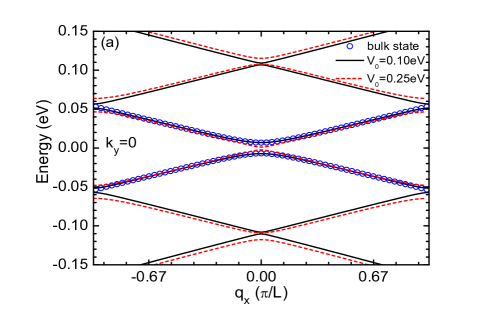
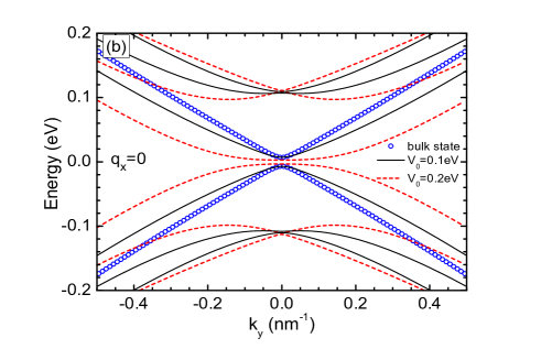
In Figure 2(b), the energy dispersion along the direction is shown with . In each energy dispersion, the averaged potential energy is subtracted. The bulk bands are also shown in Figure 2 as open symbols. When is small, the shape of bands and are close to the bulk bands as expected. We wish to point out that when the sign of is reversed, the energy dispersion is qualitatively unchanged.
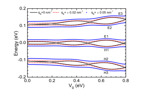
The energy dispersion changes in a rather complicated way when the barrier potential changes. In Figure 3, six energy levels are shown as a function of , with the average potential subtracted, for various values of and a fixed . One can clearly see that all bands display an oscillatory behavior. There are three critical values of the potential at which the and bands (E2 and E3, H2 and H3) touch each other when . The oscillation amplitude will be smaller and no touching point exists when or .
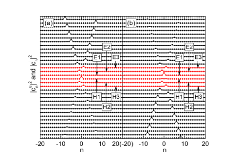
Next, we study the spatial dependence of wave functions. The system considered is uniform along the direction, therefore we only need to investigate the probability distribution along the direction. The total distribution, for a specific band, can be written as contributed from the upper and lower components of the corresponding wave function. Figure 4 shows the probability distribution for various value of and with a fixed eV. The well/barrier regions are indicated by two vertical lines in Figure 4. Figure 4(a) is for the band and Figure 4(b) for the band. It can be seen that, for the band, the amplitude of wave function in the middle well region () is larger than that in the barrier region ( and ). But for the band, the amplitude of wave function is larger in the barrier region.
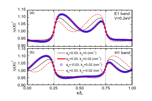
It is interesting to note that the energy of and bands is about eV, both below the barrier potential eV. On the other hand, the distribution shows that the band behaves like a state in the well, while the band behaves like a state in the barrier, if we view them in a traditional single band picture. In the single band case, when the band energy is below the barrier of a superlattice potential, the wave function should be more confined in the well region. The result shown in Figure 4 indicates that a state whose energy is below the barrier could become “localized” in the well region or in the barrier region. This resembles the case of above-barrier states in a semiconductor superlattice Colak and Shahzad (1988); Zhang et al. (1992, 1993); Tseng et al. (2001). This effect is not unexpected, as in the present study, we deal with a two-band model with a strong inter-band coupling.
As shown in Figure 4, electronic states with have a symmetrical distribution about the center of the unit cell . This symmetry will be destroyed if . However, the distribution of a state with and the distribution of a state with are connected by a reflection transformation about the center of the unit cell. By making the reflection transformation, one obtains the distribution for from the distribution for and vice versa. This symmetry about the distribution is due to the symmetry of the model Hamiltonian that .
Next, we study how the probability distribution (the wave function) changes when the lateral superlattice potential changes. This task becomes easier if we introduce the notion of probability distribution integrated over the well region in an unit cell with and . Similarly, we also introduce the probability distribution integrated over the barrier region in an unit cell. In Figure 5, we show the total for the and bands for various values of , and . It is clear that, as the barrier potential increases, the probability distribution in the well displays an oscillatory behavior around the homogenous value. When , the oscillation of shows abrupt changes at several values of (see Figure 5(a) and also Figure 5(d)). When , these abrupt changes becomes smoother.
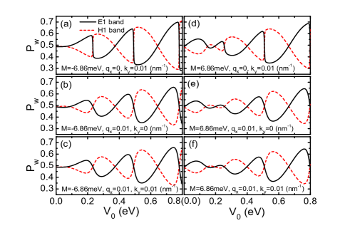
The integrated probability distribution for the , , , and bands are shown in Figure 6 for nm-1, and two values of .
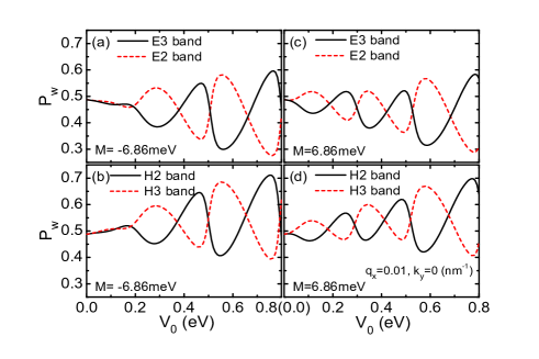
The oscillatory behavior is similar to that of and bands except that the oscillation is slightly slantwise to the homogeneous distribution. States with even higher/lower energies are also investigated and similar results are found. This result is consistent with that in Reference Gao et al. (2011), where the author found that the spin polarization oscillates across the boundary of a step-function electrical potential on the surface of a three dimensional topological insulator and is not confined by the potential due to the Klein paradox. By examining Figure 5 and 6, one observes that the amplitude of the oscillation is not strong and this indicates that the effectiveness of gating on top of a 2D topological insulator is limited. As we have mentioned, this is due to the coupled two-band nature intrinsic to the system. Moreover, it should be pointed out that the oscillatory pattern can be modified dramatically when a different set of topological insulator parameters Zhou et al. (2008) is used.
It is well-known that, when the effective model for the 2D topological insulator is applied to a stripe geometry system, the existence of the nontrivial edge states requires that the bulk bands must be inverted, i.e., Zhou et al. (2008). When all parameters except are unchanged, the model with negative and positive have completely different behavior when applied to the stripe system. In Figure 5 and 6, we compare calculated with a negative and a positive one. The left panels are for the negative case and the right panels are for the positive case. In the case of positive , one observes that the number of oscillations increases. However, it is clear that there is no significant difference between two cases.
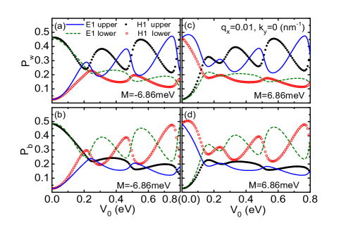
As the lateral superlattice studied in this paper is a coupled two-band system, we have evaluated the probability distribution for each component of a state. In Figure 7, the integrated probability distribution (wave function) is shown for the upper and lower component of wave function separately. The integral is performed either inside the potential well region (Figures 7(a) and 7(c)) or in the barrier region (Figures 7(b) and 7(d)). Only the results for the and bands are presented. In the left panels , and in the right panels . nm-1 and . One observes that the two components both display oscillatory behavior.
In the case of (Figures 7(a) and 7(b)), when is small, and of the band mainly consists of the upper component, and for the band they are dominated by the lower component. As increases, the difference between two components becomes small. In contrast, when (Figures 7(c) and 7(d)) and is small, the band is mainly contributed from the upper component and the band is dominated by the lower component. More calculations show that when and becomes large, the contribution to and from upper and lower components will become nearly the same, even in the region of small .
IV Summary
In summary, we have investigated theoretically the properties of electronic states of a lateral superlattice made of a 2D topological insulator. The dispersion of mini-band and the electron wave function in the potential well region are found to display an oscillatory behavior as the potential strength of the lateral superlattice increases. The probability of finding an electron in the potential well region can be larger or smaller than the average as the potential strength varies. This indicates that the electrical confining effect in two-dimensional topological insulators is not high and one should be careful with the idea of creating boundaries using gate voltage in device design. These features are different from that in a single-band Kronig-Penney model, and can be attributed to the coupled-multiple-band nature of the 2D topological insulator model.
Acknowledgements.
This work was partly supported by NSF and MOST of China.References
- Zhang (2008) S.-C. Zhang, Physics 1, 6 (2008).
- Qi and Zhang (2010) X.-L. Qi and S.-C. Zhang, Physics Today 63, 33 (2010).
- Hasan and Kane (2010) M. Z. Hasan and C. L. Kane, Rev. Mod. Phys. 82, 3045 (2010).
- Moore (2010) J. E. Moore, Nature 464, 194 (2010).
- König et al. (2007) M. König, S. Wiedmann, C. Brüne, A. Roth, H. Buhmann, L. W. Molenkamp, X.-L. Qi, and S.-C. Zhang, 318, 766 (2007).
- Hsieh et al. (2008) D. Hsieh, D. Qian, L. Wray, Y. Xia, Y. S. Hor, R. J. Cava, and M. Z. Hasan, Nature 452, 970 (2008).
- Analytis et al. (2010) J. G. Analytis, R. D. McDonald, S. C. Riggs, J.-H. Chu, G. S. Boebinger, and I. R. Fisher, Nat. Phys. 6, 960 (2010).
- Zhang et al. (2010a) L. B. Zhang, K. Chang, X. C. Xie, H. Buhmann, and L. W. Molenkamp, New Journal of Physics 12, 083058 (2010a).
- Zhang et al. (2010b) L. B. Zhang, F. Zhai, and K. Chang, Phys. Rev. B 81, 235323 (2010b).
- Jiang et al. (2010) Z.-F. Jiang, R.-L. Chu, and S.-Q. Shen, Phys. Rev. B 81, 115322 (2010).
- Zhang et al. (2011) L. B. Zhang, F. Cheng, F. Zhai, and K. Chang, Phys. Rev. B 83, 081402 (2011).
- Dolcini (2011) F. Dolcini, Phys. Rev. B 83, 165304 (2011).
- Citro et al. (2011) R. Citro, F. Romeo, and N. Andrei, Phys. Rev. B 84, 161301 (2011).
- Zhang and Ting (2012) D. Zhang and C. S. Ting, Phys. Rev. B 85, 115434 (2012).
- Michetti et al. (2012) P. Michetti, J. C. Budich, E. G. Novik, and P. Recher, Phys. Rev. B 85, 125309 (2012).
- Wang et al. (2012) J. Wang, X. Chen, B.-F. Zhu, and S.-C. Zhang, Phys. Rev. B 85, 235131 (2012).
- Romeo et al. (2012) F. Romeo, R. Citro, D. Ferraro, and M. Sassetti, Phys. Rev. B 86, 165418 (2012).
- Yokoyama et al. (2010) T. Yokoyama, A. V. Balatsky, and N. Nagaosa, Phys. Rev. Lett. 104, 246806 (2010).
- Gao et al. (2011) J.-H. Gao, J. Yuan, W.-Q. Chen, Y. Zhou, and F.-C. Zhang, Phys. Rev. Lett. 106, 057205 (2011).
- Bernevig et al. (2006) B. A. Bernevig, T. L. Hughes, and S.-C. Zhang, 314, 1757 (2006).
- Zhou et al. (2008) B. Zhou, H.-Z. Lu, R.-L. Chu, S.-Q. Shen, and Q. Niu, Phys. Rev. Lett. 101, 246807 (2008).
- Li et al. (2009) J. Li, R.-L. Chu, J. K. Jain, and S.-Q. Shen, Phys. Rev. Lett. 102, 136806 (2009).
- Chang and Lou (2011) K. Chang and W.-K. Lou, Phys. Rev. Lett. 106, 206802 (2011).
- Krueckl and Richter (2011) V. Krueckl and K. Richter, Phys. Rev. Lett. 107, 086803 (2011).
- Schmidt et al. (2009) M. J. Schmidt, E. G. Novik, M. Kindermann, and B. Trauzettel, Phys. Rev. B 79, 241306 (2009).
- Novik et al. (2010) E. G. Novik, P. Recher, E. M. Hankiewicz, and B. Trauzettel, Phys. Rev. B 81, 241303 (2010).
- Krueckl and Richter (2012) V. Krueckl and K. Richter, Phys. Rev. B 85, 115433 (2012).
- Takagaki (2012) Y. Takagaki, Phys. Rev. B 85, 155308 (2012).
- Dombey and Calogeracos (1999) N. Dombey and A. Calogeracos, Physics Reports 315, 41 (1999).
- Masir et al. (2010) M. R. Masir, P. Vasilopoulos, and F. M. Peeters, Journal of Physics: Condensed Matter 22, 465302 (2010).
- Colak and Shahzad (1988) S. Colak and K. Shahzad, Phys. Rev. B 38, 9667 (1988).
- Zhang et al. (1992) F. C. Zhang, N. Dai, H. Luo, N. Samarth, M. Dobrowolska, J. K. Furdyna, and L. R. Ram-Mohan, Phys. Rev. Lett. 68, 3220 (1992).
- Zhang et al. (1993) F. C. Zhang, H. Luo, N. Dai, N. Samarth, M. Dobrowolska, and J. K. Furdyna, Phys. Rev. B 47, 3806 (1993).
- Tseng et al. (2001) S. M. Tseng, Y. F. Chen, Y. T. Cheng, C. W. Hsu, Y. S. Huang, and D. Y. Lin, Phys. Rev. B 64, 195311 (2001).