Giant electroresistance and tunable magnetoelectricity in a multiferroic junction
Abstract
First-principles density functional calculations show that the multiferroic junction with asymmetric (RuO2/PbO and TiO2/SrO) interfaces has a large ferroelectric depolarizing field, whose switching changes the interface transmission probabilities for tunneling electrons, leading to electroresistance modulation over several orders of magnitude. The switching further affects the interface spin density, naturally driving magnetoresistance as well as modulated spin-dependent in-plane resistivity, which may be exploited in field-effect devices.
pacs:
73.40.-c,77.80.Fm, 85.50.-n, 75.70.-iI introduction and method
Multiferroic junctions are stacks of metallic ferromagnets and insulating ferroelectrics where electroresistance and magnetoresistance modulationkey-1 ; key-3 have been obtained via polarization switching in the ferroelectric interlayer. Ferroelectric (FE) materials –especially perovskite oxides– are used as tunnel barriers between metal electrodes. Polarization charges accumulate at the interfaces of the finite FE layer with the rest of the stack, and cause a depolarizing field in the FE. Despite the strong screening by the metal electrodes, a sizable field survives in typical junctions. This persistence is the basis for nanoscale device concepts for data storage.key-23 ; key-38 ; key-39 A large (“writing”) external bias across the FE is used to switch the FE depolarizing field and polarization, and a small (“reading”) bias is then used to read the resistance of the stack in the newly realized state. This resistance may –in fact, in the present case, does– depend on polarization (i.e. depolarizing field) orientation, for instance because of interface structure or of asymmetries in potential profile along the junction and the associated tunneling probability. If that is the case, an electroresistance effect is realized.
When ferromagnetic (FM) electrodes are added to the junction, a multiferroic tunnel junction (MFTJ) is realized. Electron tunneling from the electrode through the FE barrier is now spin-dependent, and the tunneling current also depends on the relative orientation of magnetization of the two electrodes, or on the local induced magnetization. Thus, in MFTJs, tunneling magneto- and electro-resistance (TMR and TER) effects coexist, leading to four distinct states accessible via electric and magnetic external fields.key-26 ; key-27
Further, because of the same asymmetries, the interface polarization charge is spin-polarized to a degree depending on polarization direction. MFTJs may thus exhibit interfacial magneto-electricity (ME), i.e. changes in interface magnetization induced by FE polarization reversal, hence ultimately driven by an electric field.key-28 ; key-17 The polarization switching changes sign and value of the FE charge at a given interface, but also its relative majority or minority spin content, establishing a tunable interface magnetization. Of course, this will affect both the tunneling (typically ballistic) and the in-plane (typically diffusive) transport in either spin channel.
In this paper, we study with first-principle calculations a (SRO/PTO/SRO) multiferroic tunnel junction, and specifically its tunneling electroresistance, interfacial ME coupling, and in-plane transport. Due to the chemical asymmetry of the interfaces and the strong polarization of the FE layer, the electroresistance modulation is up to two orders of magnitude larger than in previous studies on BaTiO3-based MFTJs.key-26 ; key-20 We also find a smaller but potentially useful tuning of in-plane resistance, originating from polarization-induced magnetization changes. Interface ME is present, with coupling coefficients similar to other MFTJs. key-21
The electronic and atomic structure of the SRO/PTO/SRO junction is calculated within density functional theory in the generalized gradient (GGA) approximation and the projector augmented wave (PAW) as implemented in the VASP code.key-25 PTO has been relaxed in tetragonal symmetry, obtaining =3.924 Å, =4.176 Å, Ti-O on-axis bonds 1.79 Å and 2.38 Å, FE energy gain over paraelectric 108 meV, polarization P=0.86 C/m2. PTO cells with this structure and cubic SRO have been stacked keeping the in-plane lattice constant of PTO. The two interfaces between insulator and metal, /PbO at one side and /SrO at the other, are labeled ‘Ru’ and ‘Ti’ below and are simulated in an in-plane 22 section. The supercell has 7 layers of PTO and 6 layers of SRO as short-circuited ferromagnetic electrode, for a total of 260 atoms. We consider the two ferroelectric states of PTO with polarization P pointing in opposite directions, perpendicular to the interfaces; all the quantities pertaining to P pointing from RuO2/PbO to the TiO2/SrO (“Ru to Ti”) are depicted in blue, while those for P pointing from TiO2/SrO to RuO2/PbO (“Ti to Ru”) are in red. All configurations are reoptimized in length and relaxed with force tolerance 40 meV/Å, using a 4×4×1 k-point Monkhorst-Pack mesh.
II Results
II.1 Charge and potential
To analyze the total charge density (built adding narrow Gaussian charges at the ions location to the electronic charge) and electrostatic potential in the junction in the two polarization states, we feed their average over the sectional area =4 of our 22 planar cell to a one-dimensional square-wave filter to obtain the macroscopic averagekey-6
| (1) |
Similarly to Ref.key-2, , we extract the monopole component of the macroscopically averaged density as
| (2) |
combining the density profiles and for the two P states ( is chosen to minimize the monopoles and ends up near the midpoint of the FE layer).
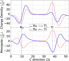
The results are shown in Fig.1. Firstly, there is a significant net accumulation of charge at the two interfaces, due to the interface polarization discontinuity charge screened by the metal electrons and by the ionic response in both the insulator and the metal; the monopole is quite delocalized in comparison to that at semiconductor interfaces.key-2 This local charge produces a depolarizing field 5108 V/m in the FE layer, which can be read off the potential profile in Fig.2, as well as from the local density of states (Fig.3) discussed below. For a finite polarized PTO slab of this thickness, the expected depolarizing field would be about 9108 V/m assumingdc a static dielectric constant 100. The large residual field indicates that the metallic screening is incomplete, as suggested earlier.key-23 ; key-26

Secondly, the asymmetric interfaces of highly polarized PTO produce quite different potential profiles for the two polarization directions, without any symmetry-breaking layer of other materials interposed between electrode and barrier.key-20 This implies that the tunneling resistance along the junction will be changed by the switching of PTO polarization. As suggested by simplified models,key-14 for such asymmetric potential and large residual electric field one expects a strong TER effect, which we now demonstrate calculating a) the semiclassical tunneling conductance through the 1D potential profile of the junction, and b) the transmission coefficient from the evanescent-wavefunction ratio in the insulator.
II.2 Tunneling electroresistance: WKB
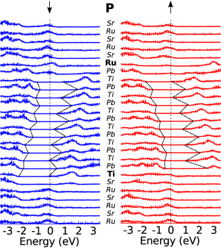
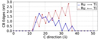
To quantify the TER in our junction, we first study the semiclassical tunneling conductance through the 1D potential profile of the junction. An appropriate model for the potential profile through which the electrons tunnel is the position-dependent conduction band edge of the junction referred to Fermi energy . To extract this profile, we calculate for the two polarization orientations the layer-resolved local density of states (LDOS), which is displayed in Fig.3. The position dependent PTO band edges shift along the junction at a rate determined by the depolarizing field, whose value is in the mid 108 V/m as already indicated by the averaged potential profile. We then extract from the LDOS the position of the conduction edge in each layer, and use it to construct the potential profiles for the two values of P, which, as shown in Fig.4, are strongly asymmetric.
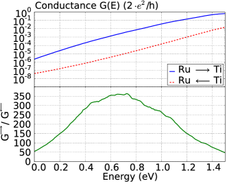
We then calculate the tunneling probability in the semiclassical Wentzel-Kramers-Brillouin approximation through these two profiles vs. injection energy, choosing the Fermi energy as zero. (This describes electrons tunneling into the PTO conduction band. Hole tunneling is neglected due to the large barriers and effective masses.) As shown in Fig.5 the ratio /, i.e. the TER, is between 50 and 350 depending on energy, and therefore up to two orders of magnitude larger than in BaTiO3/SRO junctions.key-26 The absolute values of are comparable with those found for similar junctions. We note that if we roughly estimate the writing voltage needed to reverse the depolarizing field in this structure as the field times the PTO thickness we find 2 V; thus, it would be safe to use a standardchou reading voltage of 0.5-0.6 V, which would yield a near-maximum TER.
II.3 Tunneling electroresistance: Transmission function
The second indication of a giant TER effect comes from the two transmission functions across the two interfaces in the two poling directions. For not too thin a barrier, the transmission function of a tunnel junction could be factorizedkey-15 as
| (5) |
where is the barrier thickness, is the lowest decay rate in the barrier and are the transmission probabilities from the left or right electrode into the barrier across the interfaces (Ru or Ti respectively) for an electron with a given , for both polarization directions.
In our junction, the two interfaces differ both chemically and electrostatically depending on the direction of polarization, hence we have four different ’s to assess. Assuming the same exponential decay for the two polarizations, we have
| (6) |
The two ratios can be extracted from the ratio of the density of metal-induced gap states at distance from the two interfaces for the two poling directions, i.e.
| (7) |
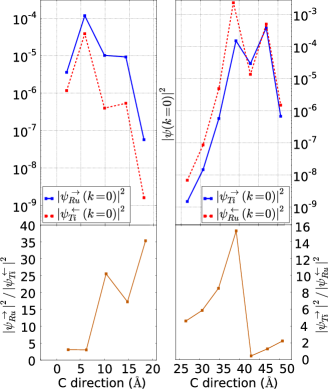
The upper panels of Fig.6 shows the wavefunctions as function of for =0 at the Fermi energy along the junction for the two polarization directions, and the lower panels display their ratios. Thus, /25 and /10, so that the transmission ratio is about 250, a measure of the TER comfortingly similar to the WKB result shown above.
II.4 Interface barriers and the origin of asymmetry
The asymmetry giving rise to the large TER is of electronic origin. This can be seen from the LDOS in Fig.3: at the Ru-Sr-Ti interface (bottom right in Fig.3), the PbO layer opposes a large barrier to tunneling, while the TiO2 layer adjacent to SRO is metallized; at the Ru-Pb-Ti interface (top left in Fig.3) the PbO layer in contact with SRO is metallized, and the first barrier is the smaller one provided by the TiO2 layer. Put differently, the conduction Schottky barriers between SRO and PTO for the two interfaces are different; indeed, our estimated difference in the conduction edge position at the interface agrees with the calculatedumeno 0.7 eV difference between Schottky barriers of the two interfaces.nota Since despite the gap underestimate in GGA this difference is well reproduced, both the TER and the absolute tunneling conductance should be considered quite accurate. We conclude that the smaller TER asymmetry in SRO/BaTiO3 is related to its lesser or absent Schottky barrier asymmetry.jg
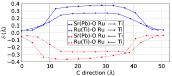
Ionic screening, in turn, presents no significant surprise: cationic displacements in the junction are rather well behaved, as shown by Fig.7; they agree largely with previous estimatesumeno and are fairly similar to BTO/SRO (although here they are larger on average consistently with the larger polarization of PTO).
II.5 Interface magnetoelectricity
We now consider the interface ME effect. We elect to estimate the interface ME coefficient assuming a linear magnetization-field relation
| (8) |
Given the likely importance of non-linearity for the high fields involved here, this should be considered an order-of magnitude estimate. There is some latitude in deciding which magnetization changes are to be considered, depending on the operational procedure or application envisaged. In the present context, the natural scenario is polarization switching: is the integrated difference of magnetization density at each interface between the two polarization states. Clearly, two interface-related ME coefficients will result, either one of which will be relevant in practice depending on which interface is active in the specific experiment or application. To operationally implement this scenario, one just needs to switch P via the writing voltage.
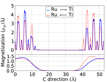
To calculate the ’s we define in analogy to the charge density in Sec.II.1 the macroscopic averages of the magnetization density () and () for the two states RuTi and RuTi of PTO polarization. In Fig.8 we report the planar and macroscopic averages for the two P states. Upon switching, the magnetization changes strongly at the Ti interface, much less at the Ru one.
To calculate the ’s we conventionally choose the initial P state to be RuTi and the final state RuTi. The magnetization changes at the Ru or Ti interface are
| (9) |
where the integrals are done near each interface between the region of zero magnetization within PTO and the region of constant magnetization within SRO, specifically (see Fig.8) between 2 and 21 Å for the Ru interface, and 31 and 49 Å for the Ti interface. We choose as electric field in Eq.8 the depolarizing field , which is taken positive by convention (a different choice will simply change the sign of both ME coefficients). We then obtain the ME coefficients as
| (10) |
Table 1 summarizes the induced magnetizations (Eq.9) and the ME coefficients at the two interfaces (Eq.10). Again the asymmetry in the interfaces shows up dramatically. The ME coefficients are somewhat smaller than those predicted for other similar MFTJs,key-17 ; key-21 despite our induced magnetizations being larger. This is due to our assuming conservatively a switching electric field larger than typical operational coercive fields of PTO. These may be 5 to 20 times smaller depending on external conditions and sample properties (and hence the could be larger by the same factors).
| Interface | ||
|---|---|---|
| Ru | –0.31 | –0.11 |
| Ti | 4.46 | 1.62 |
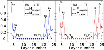
Some additional insight can be gained by examining in Fig.9 the atom-resolved average magnetic moments obtained integrating the magnetization density within atomic spheres defined by the PAW construction. Consistently with its larger ME coefficient, the Ti interface (right side of each panel) is more magnetically polarizable than the Ru interface. For RuTi polarization (right panel), magnetization builds up in the first Ru layers, spilling over into the Ti metallized layer and through to the first insulating PbO layer. In RuTi polarization (left panel), the interface Ru’s lose some (and Ti and oxygens, all) of their moment. At the Ru interface (left side of each panel), the magnetization does not extend at all into PTO (specifically in the PbO layer) in either case, and the SRO magnetization mostly redistributes among Ru’s and O’s in the first and second layer, changing only slightly overall (see also Fig.8).
In closing this Section, we note that another possible choice for is the interface magnetization density change with respect to zero electric field. In our case, this translates into the magnetization difference at the two interfaces with or without the depolarizing field, i.e. for ferroelectrically-distorted or paraelectric PTO. As P, i.e. the field, can be turned on in two ways, this procedure produces four ME coefficients, =0.62, =0.14, =1.75, in units of 10-11Gcm2/V. This polarization “turn-on” scenario, unfortunately, is essentially impracticable. It would require forcing PTO across its ferroelectric transition, e.g. by lowering the temperature across the Curie point Tc, with a small poling voltage applied to the junction to select the desired P state. This is largely incompatible with device operation due to the high Tc500∘ C.
II.6 In-plane conductivity modulation
The sizable interface asymmetry and ME coupling will influence the in-plane current in the SRO layer. To assess this effect, we use the BoltzTraPkey-16 code to calculate the conductivity in the plane of the junction in the diffusive regime as
| (11) |
with
| (12) |
where is a band index, a relaxation time, the group velocity calculated from the band structure, and the occupation function. Assuming constant, we can plot / vs chemical potential. Although the scattering mechanisms may not be described in full detail, this approximation is quite sufficient to address conductivity ratios between polarization states. (We note in passing that diffusive conductivity is appropriate for in-plane transport, but may be inapplicable to tunneling transport depending on the nature of the Fermi surface of the junction system. In the present case this approach gives a TER 105 which, while consistent with similar calculations for 1+6 PTO/SRO superlattices,callori is probably significantly overestimated.)
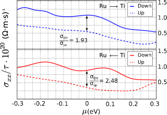
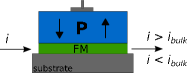
The in-plane spin-resolved conductivity in the diffusive regime in the two polarization states is shown in Fig.10. The total conductivity changes by 35% upon polarization switching. Also, the switching modulates the down to up-spin conduction ratio (2.5 to 1.9) by 15% compared to the calculated bulk value (2.2). Such sizable modulations may be employed in in-plane field-effect devices such as that sketched in Fig.10.
The electrically-stored polarization orientation could be read electrically from the current modulation in the metal channel, i.e., effectively, as a modulated resistivity; this could be done either with the total current, or one of the spin components if polarized contacts are used. Another application of this configuration may be a filter or modulator of the incoming current, measuring the outgoing spin-polarized current calibrated to that of the bulk.
Note that our calculations measure the conduction within the whole PTO/SRO layer system, and there is no way to single out the net contribution of each interface; the exact values of the modulation will thus depend on SRO thickness, and will change if one of the interfaces (e.g. SRO/substrate) is “ferroelectrically dead”.
III Summary
In conclusion, we considered a multiferroic tunnel junction with asymmetric interfaces and a large-polarization FE. Very different potential profiles result for the two polarization states, and lead to a giant TER of up to 350. The interface charge accumulation is spin-polarized, with magnetization and magnetization changes depending on the interfaces and on polarization orientation, with sizable ME coefficients. The ME coupling affects the in-plane diffusive transport of the junction changing the majority to minority conductivity ratio, as well as the total conductivity. In particular, upon P inversion, the conductivity is modulated by 35% and its spin polarization by 15%, which is presumably exploitable in practical applications. In forthcoming work we plan to study TMR, which may be expected to be high also, as well as the effects of magnetic doping of the FE layer.
Acknowledgments
Work supported in part by MIUR-PRIN 2010 Oxide, IIT-Seed NEWDFESCM and POLYPHEMO, IIT “platform computation”, Fondazione Banco di Sardegna, and CINECA.
References
- (1) E. Y. Tsymbal, A. Gruverman, V. Garcia, M. Bibes and A. Barthélémy, MRS Bull. 37, 138 (2012).
- (2) K. F. Wang, J.-M. Liu, and Z. F. Ren, Adv. Phys. 58, 321 2009.
- (3) J. Junquera and P. Ghosez, Nature 422, 506 (2003).
- (4) V. Garcia, S. Fusil, K. Bouzehouane, S. Enouz-Vedrenne, N.D. Mathur, A. Barthélémy, M. Bibes, Nature 460, 81 (2009).
- (5) A. Gruverman, D. Wu, H. Lu, Y. Wang, H.W. Jang, C.M. Folkman, M.Y. Zhuravlev, D. Felker, M. Rzchowski, C.-B. Eom, E.Y. Tsymbal, Nano Lett. 9, 3539 (2009).
- (6) J. P. Velev, C.-G. Duan, J. D. Burton, Alexander Smogunov, M. K. Niranjan E.Tosatti, S. S. Jaswal, and E. Y. Tsymbal, Nano Lett. 9, 427 (2009).
- (7) M. Y. Zhuravlev, S. Maekawa and E. Y. Tsymbal, Phys. Rev. B 81, 104419 (2010).
- (8) C.-G. Duan, S. S. Jaswal, and E. Y. Tsymbal, Phys. Rev. Lett. 97, 047201 (2006).
- (9) C.-G. Duan, J. P. Velev, R. F. Sabirianov, Z. Zhu, J. Chu, S. S. Jaswal, and E. Y. Tsymbal, Phys. Rev. Lett. 101, 137201 (2008).
- (10) N.M. Caffrey, T. Archer, I. Rungger and S. Sanvito, Phys. Rev. Lett. 109, 226803 (2012).
- (11) M. K. Niranjan, J. D. Burton, J. P. Velev, C.-G. Duan, S. S. Jaswal, and E. Y. Tsymbal, Appl. Phys. Lett. 95, 052501 (2009).
- (12) G. Kresse and J. Furthmüller, Phys. Rev. B 54, 11169 (1996); G. Kresse and D. Joubert, ibid. 59, 1758 (1999).
- (13) M. Peressi, N. Binggeli, and A. Baldereschi, J. Phys. D: Appl. Phys. 31, 1273 (1998).
- (14) F. Bernardini and V. Fiorentini, Phys. Rev. B 57, R9427 (1998).
- (15) W. Guo, D. Jin, W. Wei, and H. J. Marisa, J. Appl. Phys. 102, 084104 (2008); Ø. Dahl, J. K. Grepstad, and T. Tybella, J. Appl. Phys. 103, 114112 (2008).
- (16) M. Y. Zhuravlev, R. F. Sabirianov, S. S. Jaswal, and E. Y. Tsymbal, Phys. Rev. Lett. 94, 246802 (2005).
- (17) A. Chanthbouala, A. Crassous, V. Garcia, K. Bouzehouane, S. Fusil, X. Moya, J. Allibe, B. Dlubak, J. Grollier, S. Xavier, C. Deranlot, A. Moshar, R. Proksch, N. D. Mathur, M. Bibes, and A Barthélémy, Nature Nanotech. 7, 101 (2011).
- (18) K. D. Belashchenko, E. Y. Tsymbal, M. van Schilfgaarde, D. A. Stewart, I. I. Oleynik, and S. S. Jaswal, Phys. Rev. B 69, 174408 (2004).
- (19) Y. Umeno, J. M. Albina, B. Meyer, and C. Elsässer, Phys. Rev. B 80, 205122 (2009).
- (20) We obtain a similar value using the standard procedure of Ref.key-6, for non-polar PTO. The monopole component could not be completely eliminated from the potential profile in the polar case, leading to large uncertainties in the final value.
- (21) P. Ghosez and J. Junquera, in Handbook of theoretical and computational nanotechnology, M. Rieth and W. Schommers eds. (American Scientific Publishers, Valencia, USA, 2006), ch. 134.
- (22) J. M. Rondinelli, M. Stengel and N. Spaldin, Nat. Nanotech. 3, 46 (2008).
- (23) G. K. H. Madsen and D. J. Singh, Comput. Phys. Commun. 175, 67 (2006).
- (24) S. J. Callori, J. Gabel, D. Su, J. Sinsheimer, M. V. Fernandez-Serra, and M. Dawber, Phys. Rev. Lett. 109, 067601 (2012).