Electric-field induced domain-wall dynamics: depinning and chirality switching
Abstract
We theoretically study the equilibrium and dynamic properties of nanoscale magnetic tunnel junctions (MTJs) and magnetic wires, in which an electric field controls the magnetic anisotropy through spin-orbit coupling. By performing micromagnetic simulations, we construct a rich phase diagram and find that, in particular, the equilibrium magnetic textures can be tuned between Néel and Bloch domain walls in an elliptical MTJ. Furthermore, we develop a phenomenological model of a quasi-one-dimensional domain wall confined by a parabolic potential and show that, near the Néel-to-Bloch-wall transition, a pulsed electric field induces precessional domain-wall motion which can be used to reverse the chirality of a Néel wall and even depin it. This domain-wall motion controlled by electric fields, in lieu of applied current, may provide a model for ultra-low-power domain-wall memory and logic devices.
pacs:
75.78.Fg, 75.85.+t, 75.78.Cd, 85.75.-dI Introduction
Spin-transfer torque (STT) Slonczewski (1996); *Berger96 has emerged as an effective mechanism to control memory and logic devices such as magnetic tunnel junction (MTJ)-based nonvolatile magnetic random-access memory Chen et al. (2010) and domain-wall-based race-track memory.Parkin et al. (2008) However, the spin-polarized currents required for these devices are notoriously high and therefore energy inefficient, prompting the search for alternate low-power electric control. One promising alternative is voltage-controlled magnetic anisotropy (VCMA), in which an applied voltage induces an excess charge at the interface between the tunnel-barrier and transition-metal ferromagnet in an MTJ. This modifies the occupation and, possibly, the character of “-like” bands in the transition metal, which, via spin-orbit coupling, modifies the anisotropy perpendicular to the insulator-ferromagnetic interface.Maruyama et al. (2009); *Duan2008; *Nakamura2008 Controlling magnetic anisotropy by applying an electric field alleviates the use of power-hungry currents in order to manipulate MTJs. For instance, VCMA has been shown experimentally and theoretically to assist switching by externally applied magnetic field,Shiota et al. (2009); *wangNATMAT11; *alzate12 induce precessional switching,Shiota et al. (2011) induce ferromagnetic resonance,Zhu et al. (2012) and provide control of the threshold switching current.Liu et al. (2012) On the other hand, while VCMA has been shown to modulate domain-wall velocity Schellekens et al. (2012); *Bauerand nucleation,Bernand-Mantel et al. (2013)to the best of our knowledge, inducing domain-wall motion purely by electric field has neither been theoretically proposed nor experimentally observed.
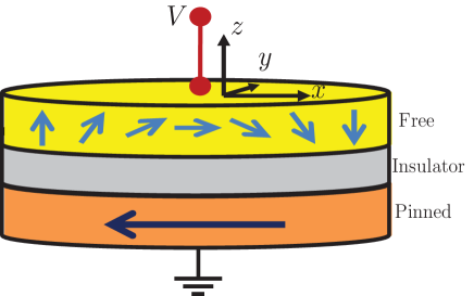
In this paper, by determining the static micromagnetic configurations and their dynamic response to electric fields, we provide a method for inducing domain-wall motion purely by electric fields. To analyze the equilibrium magnetic texture, we consider a ferromagnet(F)insulator (I)F heterostructure with an elliptical cross section, i.e., an MTJ, where one of the ferromagnetic layers is pinned and the other free. See Fig. 1. The presence of inhomogeneous stray fields from the pinned layer are essential to decrease the energy cost for out-of-plane magnetization and therefore encourage out-of-plane texture. By performing micromagnetic simulations, we find that a domain wall can be stabilized when the perpendicular anisotropy, controlled by applied voltage, overcomes the out-of-plane demagnetization field. Informed by micromagnetic simulations, we study the VCMA-induced dynamics of this confined domain-wall by analytically modeling it as a quasi-one-dimensional magnetic wire. We find that VCMA induces precessional dynamics which can be exploited to switch the chirality of a Néel domain wall or force it to escape confinement.
II Equilibrium configurations
We consider a device geometry, shown in Fig. 1, which consists of an MTJ with a free ferromagnetic layer and a pinned ferromagnetic layer, pointing along , separated by an insulator having thicknesses , , and , respectively. The cross section of the heterostructure is an ellipse where the semimajor axis is along the direction and the semiminor axis is along the direction.
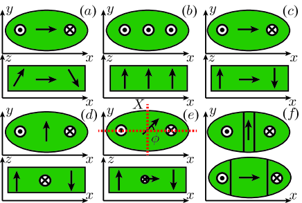
There are several magnetic configurations necessary to characterize the equilibrium states of our system as a function of perpendicular anisotropy. We schematically draw them in Fig. 2. The magnetization can be primarily in the plane of the ellipse along the axis [see Fig. 2(a)], however the texture near the edges of the ellipse tend to follow the stray fields of the pinned layer and cant out of plane at angle . If the perpendicular anisotropy is large enough, the magnetization points entirely along the axis [see Fig. 2(b)]. Fig. 2(c) and (d) depict Néel and Bloch domain walls, respectively, where the magnetic domains are along the axis. A third domain wall, we call Bloch-like, in which the magnetization in the center of the domain wall is in-plane and aligned at an angle away from the axis [see Fig. 2(e)]. A Néel (Bloch) domain wall is a limiting example of a Bloch-like wall with () and can smoothly interpolate between Néel and Bloch domain walls, as follows: When the domain-wall width (), schematically drawn in Fig. 2(f) and controlled by perpendicular anisotropy, is large the energy is minimized due to dipolar interactions when the central region points along the axis. As is decreased, becoming narrower than the semiminor axis of the ellipse, the dipole energy in the Néel wall increases, forcing the magnetization at the center of the wall to orient away from the axis to a finite value of .Jung et al. (2008); *koyama
To develop a precise numerical model using micromagnetic simulations we take the magnetization saturation emu/cm3 and exchange stiffness erg/cm. The perpendicular anisotropy is assumed to be of the form, , with erg/cm2. These choices of material parameters are typical for a CoFeB/MgO interface. Ikeda et al. (2010) For equilibrium simulations we control the perpendicular anisotropy by varying the free layer thickness. The major and minor axes are nm and nm respectively, while the thickness nm and nm. All the simulation results presented in this paper are obtained for zero temperature and are performed using the LLG Micromagnetic Simulator.LLG The phase diagram was constructed by initializing the free magnetic layer along or along the direction and allowing the system to relax to equilibrium (possibly resulting in two different configurations) for values of ranging between nm and nm. Although increasing the thickness will change the demagnetization energy and influence of the stray fields, we do not expect it to significantly change our results. Energy of these equilibrium configurations are plotted as a function of perpendicular anisotropy in Fig. 3.
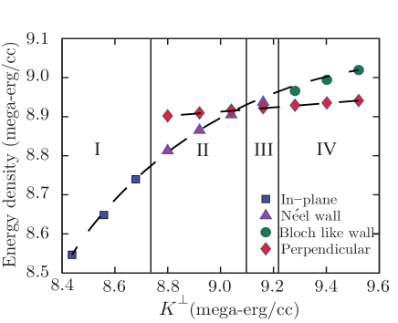
When the thickness is large nm corresponding to Merg/cm3, the magnetization is primarily in-plane with canted edges and we identify the texture with the schematic in Fig. 2(a). As the perpendicular anisotropy increases, increases until Merg/cm3 when the out-of-plane perpendicular anisotropy field overcomes the demagnetization field resulting in two stable magnetic configurations. The ground state is a Néel domain wall while we find an additional metastable state with magnetization perpendicular to the interface. The domain wall width decreases monotonically with increasing perpendicular anisotropy and at Merg/cm3 the energy of the Néel domain-wall configuration surpasses that of the perpendicular state, which is now the most energetically favorable configuration. Although the perpendicular state remains the ground state, when Merg/cm3 the metastable Néel state undergoes a second-order phase transition to the Bloch-like wall with symmetry broken between and . Further increasing the perpendicular anisotropy shrinks the domain wall, thus increasing . This control of with perpendicular anisotropy will be central in the discussion of dynamics in the following sections.
III Electric-field induced domain-wall dynamics
In this section we consider the dynamic response of Néel wall configuration to voltage. First we focus on the micromagnetics governed by the Landau-Lifshitz-Gilbert (LLG) equationPitaevskii and Lifshitz (1980); *gilbertIEEEM04 then, informed by these numerical results, we develop a phenomenological quasi-one-dimensional model, based on the Walker ansantz,Schryer and Walker (1974) and find qualitative agreement between the two.
Micromagnetics—The dynamic simulations are performed using the LLG equation:
| (1) |
where m is the unit vector pointing along the position-and time-dependent magnetization configuration of the free layer, is the Gilbert damping and is the gyromagnetic ratio. The effective field, , includes contributions from demagnetization field, exchange field and anisotropy field. In particular, VCMA torque enters due to electric field dependent anisotropy field which is taken into account by making , in line with recent experiments, where is the electric field. The magneto-electric coupling coefficient is taken to be erg/Vcm (close to the experimentalEndo et al. (2010); Wang et al. (2012); Zhu et al. (2012) and theoretical valueNiranjan et al. (2010)), and nm, while leaving all other parameters as in the previous section. Because we are primarily interested in low dissipation devices, we include the Gilbert damping but do not include other dissipative torques (e.g. spin transfer torque) allowed by symmetry.Hoffman et al. (2012) We initialize the system so that the free layer is a Néel domain wall which, for these parameters, is the ground state of our system. To induce motion we turn on an electric field abruptly to a non zero value and allow the domain wall to equilibrate to a new equilibrium state. We summarize the resultant motion in Fig. 4.
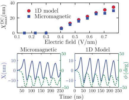
The top panel of Fig. 4 shows the maximum deviation of the domain wall, , from its equilibrium at the center of the ellipse as a function of the electric field magnitude. Below some critical value of electric field V/nm, domain-wall motion is not induced, i.e. . However when the magnitude of the electric field exceeds , the domain wall position and angle oscillate, differing by a phase, as shown in the lower left hand panel of Fig. 4. Note that the time axis in the lower left hand panel begins at ns because below this time the dynamics are dominated by high frequency modes wherein the long-time dynamics of the domain-wall position, , and tilt, are ill-defined. Importantly, corresponds to a perpendicular anisotropy of Merg/cm3 which is near the value of perpendicular anisotropy where the domain wall transitions from Néel to Bloch-like (see Fig. 3). That is, below the critical field an electric field pulse will change the width of the Néel wall but not the type of domain wall. Above the critical field the domain wall undergoes a Néel-to-Bloch-like transition, which in turn results in domain-wall motion.
1D Model— The micromagnetic simulations imply that the long-time domain-wall dynamics are dominated by the soft modes which can be characterized by the generalized coordinates and [see Fig. 2(e)] . To construct a phenomenological model of the domain-wall motion, we begin by writing down the free energy density consistent with the symmetries of our device geometry which is invariant under a mirror transformation in the plane as well as a mirror transformation in the plane followed by a rotation around the axis. Because under the former and under the latter, only even contributions of and are allowed:
| (2) |
The phenomenological constant parameterizes the strength of a parabolic confining potential due to both inhomogeneous stray fields from the pinned layer and the finite size of the free layer. The relative strength of and determine the easy plane in which the domain wall rotates. Because a positive is required for a smooth transition of equilibrium states from Néel to Bloch wall, we henceforth take to match micromagnetic simulations. Higher order interactions and interactions of the form and are in principle allowed but not necessary to reproduce Néel and Bloch-like equilibrium configurations and are thus disregarded in the spirit of constructing a minimal model. To find the equation of motion for the generalized coordinates we use the one-dimensional Walker ansatzSchryer and Walker (1974) which states, for with and being polar and azimuthal angles, respectively, and (. The equations of motion for our generalized coordinates are immediately determined following Ref. Tretiakov et al., 2008; *Thiele:
| (3) |
where we have defined , and . Because and , the stable fixed points of Eq. (3), , depend on the value of . For all stable solutions, the domain wall is at the center of the ellipse () while the domain-wall angle takes the values
| (4) |
which correspond to a Néel, Bloch-like, and Bloch domain wall, respectively. The symmetry of the structure admits two solutions for any value of .
In this model the phenomenological anisotropy fields, and , and confining field , are implicitly dependent on the perpendicular anisotropy and hence functions of the electric field. We therefore identify with the value of electric field at which becomes negative. The observed domain-wall motion in micromagnetic simulations can then be explained as the following. If , the equilibrium position is the same for both, when electric field is on and off, and thus the domain-wall tilt, as well as the position, is always in the equilibrium resulting in no motion. However, if , for the case when the electric field is on is different from when the electric field is off. The approach of to the new equilibrium in turn induces domain-wall motion according to Eq. (3).
In order to compare with micromagnetic simulations, we numerically integrate Eq. (3), first extracting values for the phenomenological parameters: is found by comparing the displacement of the Néel domain-wall in the micromagnetics and the phenomenological model as a function of externally applied magnetic field along the axis. and can then be obtained by matching and the resonance frequency of the micromagnetics to the quasi-one-dimensional model. The dynamics of the phenomenological model are shown in the lower right hand panel of Fig. 4 showing the time dependence of a domain wall, initially in a Néel configuration, after an electric field is turned on. We find the phenomenological model qualitatively matches the micromagnetic simulations. The presented minimal model is also able to provide a reasonable quantitative estimate of , which will be useful in the following section. Full quantitative agreement with the micromagnetics would require the inclusion of additional terms in the free energy, e.g. , , which is outside the scope of the present paper.
IV Depinning and Chirality Switching
Next we study the dependence of the electric field pulse duration, , on domain-wall motion. In contrast to the previous section, is much shorter than the time for the domain-wall to reach equilibrium. By exploiting the VCMA-induced dynamics we find that a short pulsed electric field can switch the domain-wall chirality, i.e. , or induce a maximum displacement greater than the quasiequilibrium response, i.e. , for the same pulse magnitude. We comment on the application of the former to magnetic memory storage and the latter to racetrack memory.
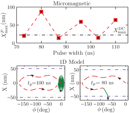
We perform micromagnetic simulations using the geometry and material parameters given in the previous section. In Fig. 5 (upper panel), we plot the maximum displacement of the domain wall, , and find an oscillatory dependence as a function of pulse length. This is similar to pulsed switching of a monodomain by an applied magnetic field:Schumacher et al. (2003) when an electric field pulse of magnitude is applied to our structure, the equilibrium domain-wall tilt changes from zero to a finite value which forces to oscillate around the new equilibrium. Because and are conjugate variables, the maximum domain-wall displacement increases with increasing tilt angle. Thus, turning off electric field pulse when is large enhances , relative to . Control of by the duration of current pulses has likewise been demonstrated for the case of spin-torque induced domain-wall motion.Thomas et al. (2006)
Chirality switching— This control of the maximum amplitude of can be used to reverse the chirality of the domain wall. See Fig. 6 (upper panel). In micromagnetic simulations we apply an electric field of magnitude 0.65 V/nm to a Néel wall initialized at which forces a new equilibrium value at . As precesses around , it goes past at which time the electric field is turned off and precesses towards the nearest Néel wall equilibrium, , switching the chirality. Likewise, we reproduce chirality switching in the phenomonological model [Fig. 6 (lower panel)]. Using the chirality to encode bit information, “0” when and “1” when , tunnel magneto-resistanceJulliere (1975) with state “0” (having resistance ) and state “1” (having resistance ) to read the chirality, and VCMA to switch it, domain-wall memory switch can be constructed. Although current-induced spin torque has also been used to switch domain-wall chirality,Vanhaverbeke et al. (2008) electric-field induced chirality switching provides a low-power attractive alternative. Moreover voltage control of chirality could provide an additional electrical knob to control recently observed efficient domain wall motion of chiral domain walls driven by spin Hall effect.Emori et al. (2013); *ryunnt13
Depinning of domain walls —We depart slightly from the free energy used in the previous sections, Eq. 2, and consider, instead of a parabolic potential , a “pinning parabolic potential” in which
| (5) |
leaving all other parameters and the equation of motion, Eq. 3, unaltered. In this potential, if the displacement of the domain wall exceeds the domain wall is no longer localized to , i.e. “depins.” Experimentally, this can be realized by depositing a pinned layer with length of the order of on top of a nanowire. Taking nm and a pulse magnitude of V/nm, we use the modified quasi-one-dimensional model to study the effect of pulse width on depinning. When ns [Fig. 5 (lower left panel)], the pulse turns off at and the domain wall returns to . A pulse width of ns [Fig. 5 (lower right panel)] ends at , displacing the domain wall further than , and depinning it. The ability to achieve depinning via pulsing electric field, in the absence of currents, could provide a major technological advantage in terms of power consumption in, for instance, racetrack memory.Parkin et al. (2008) Another key difference from the corresponding spin-torque induced domain-wall motion is the direction of electric-field induced domain-wall motion. In the present case, the domain wall can move either to or to as the new equilibrium exists at both . A small directed magnetic field, sufficient to overcome the thermal fluctuations, can break the aforementioned symmetry and favor , thus controlling the direction of motion.
V Summary
By performing micromagnetic simulations, we found that in an MTJ with high perpendicular anisotropy a domain-wall state can be stabilized either as a ground or a metastable configuration (which is assisted by inhomogeneous stray fields emanating from the pinned layer), when the perpendicular anisotropy is strong enough to overcome the long-range out-of-plane dipolar fields. These domain walls transform smoothly from Néel to Bloch structure with increasing value of perpendicular anisotropy. This transformation is driven by reduction of dipole energy stored inside the wall with decreasing domain-wall width, as the value of perpendicular anisotropy is increased. The Néel-to-Bloch-wall transormation also provides a route to induce domain-wall motion by electric field via VCMA. We developed a minimal phenomenological model explaining the oscillatory motion observed in micromagnetic simulations above a critical electric field, necessary to bring the Néel wall to the transition point of transforming into a Bloch wall. Finally, we use the predicted domain-wall motion to show that electric field pulses can be utilized to induce depinning of domain walls in magnetic wires (which in turn can be exploited in race-track like domain-wall memory devices), or achieve chirality switching (which can be used for making a domain-wall memory switch, storing information in the chirality of the domain wall or providing voltage control of chiral domain wall motion). The ability to manipulate domain walls via electric field could thus provide a path towards ultra low power magnetoelectric devices.
Acknowledgements.
This work was supported in part by the DARPA program on nonvolatile logic and by the NSF Nanosystems Engineering Research Center for Translational Applications of Nanoscale Multiferroic Systems (TANMS), Grant No. 228481 from the Simons Foundation, and the NSF under Grant No. DMR-0840965.References
- Slonczewski (1996) J. Slonczewski, J. Magn. Magn. Mat. 159, L1 (1996).
- Berger (1996) L. Berger, Phys. Rev. B 54, 9353 (1996).
- Chen et al. (2010) E. Chen, D. Apalkov, Z. Diao, A. Driskill-Smith, D. Druist, D. Lottis, V. Nikitin, X. Tang, S. Watts, S. Wang, S. Wolf, A. Ghosh, J. Lu, S. Poon, M. Stan, W. Butler, S. Gupta, C. Mewes, T. Mewes, and P. Visscher, IEEE Trans. Magn. 46, 1873 (2010).
- Parkin et al. (2008) S. S. P. Parkin, M. Hayashi, and L. Thomas, Science 320, 190 (2008).
- Maruyama et al. (2009) T. Maruyama, Y. Shiota, T. Nozaki, K. Ohta, N. Toda, M. Mizuguchi, A. A. Tulapurkar, T. Shinjo, M. Shiraishi, S. Mizukami, Y. Ando, and Y. Suzuki, Nat. Nanotech. 4, 158 (2009).
- Duan et al. (2008) C.-G. Duan, J. P. Velev, R. F. Sabirianov, Z. Zhu, J. Chu, S. S. Jaswal, and E. Y. Tsymbal, Phys. Rev. Lett. 101, 137201 (2008).
- Nakamura et al. (2009) K. Nakamura, R. Shimabukuro, Y. Fujiwara, T. Akiyama, T. Ito, and A. J. Freeman, Phys. Rev. Lett. 102, 187201 (2009).
- Shiota et al. (2009) Y. Shiota, T. Maruyama, T. Nozaki, T. Shinjo, M. Shiraishi, and Y. Suzuki, Appl. Phys. Exp. 2, 063001 (2009).
- Wang et al. (2012) W. Wang, M. Li, S. Hageman, and C. Chien, Nat. mat. 11, 64 (2012).
- Alzate et al. (2012) J. Alzate, P. Amiri, P. Upadhyaya, S. Cherepov, J. Zhu, M. Lewis, R. Dorrance, J. Katine, J. Langer, K. Galatsis, D. Markovic, I. Krivorotov, and K. Wang, in Electron Devices Meeting (IEDM), 2012 IEEE International (2012) pp. 29.5.1–29.5.4.
- Shiota et al. (2011) Y. Shiota, T. Nozaki, F. Bonell, S. Murakami, T. Shinjo, and Y. Suzuki, Nat. Mat. 11, 39 (2011).
- Zhu et al. (2012) J. Zhu, J. A. Katine, G. E. Rowlands, Y.-J. Chen, Z. Duan, J. G. Alzate, P. Upadhyaya, J. Langer, P. K. Amiri, K. L. Wang, and I. N. Krivorotov, Phys. Rev. Lett. 108, 197203 (2012).
- Liu et al. (2012) L. Liu, C.-F. Pai, D. C. Ralph, and R. A. Buhrman, ArXiv e-prints (2012), arXiv:1209.0962 [cond-mat.mtrl-sci] .
- Schellekens et al. (2012) A. Schellekens, A. van den Brink, J. Franken, H. Swagten, and B. Koopmans, Nat. Comm. 847 (2012).
- Bauer et al. (2013) U. Bauer, S. Emori, and G. Beach, Nat. Nanotech. 8, 411 (2013).
- Bernand-Mantel et al. (2013) A. Bernand-Mantel, L. Herrera-Diez, L. Ranno, S. Pizzini, J. Vogel, D. Givord, S. Auffret, O. Boulle, I. M. Miron, and G. Gaudin, Appl. Phys. Lett. 102, 122406 (2013).
- Jung et al. (2008) S.-W. Jung, W. Kim, T.-D. Lee, K.-J. Lee, and H.-W. Lee, Appl. Phys. Lett. 92, 202508 (2008).
- Koyama et al. (2011) T. Koyama, K. Chiba, D.and Ueda, K. Kondou, H. Tanigawa, S. Fukami, T. Suzuki, N. Ohshima, N. Ishiwata, Y. Nakatani, K. Kobayashi, and T. Ono, Nat. Mat. 10, 194 (2011).
- Ikeda et al. (2010) S. Ikeda, H. Miura, K.and Yamamoto, K. Mizunuma, H. D. Gan, M. Endo, S. Kanai, J. Hayakawa, S. Matsukara, and H. Ohno, Nat. Mat. 9, 721 (2010).
- (20) http://llgmicro.home.mindspring.com/.
- Pitaevskii and Lifshitz (1980) L. Pitaevskii and E. Lifshitz, Statistical Physics, Part 2: Volume 9 (Butterworth-Heinemann, 1980).
- Gilbert (2004) T. Gilbert, IEEE Trans. Magn. 40, 3443 (2004).
- Schryer and Walker (1974) N. L. Schryer and L. R. Walker, J. Appl. Phys. 45, 5406 (1974).
- Endo et al. (2010) M. Endo, S. Kanai, S. Ikeda, F. Matsukura, and H. Ohno, Appl. Phys. Lett. 96, 212503 (2010).
- Niranjan et al. (2010) M. K. Niranjan, C.-G. Duan, S. S. Jaswal, and E. Y. Tsymbal, Appl. Phys. Lett. 96, 222504 (2010).
- Hoffman et al. (2012) S. Hoffman, P. Upadhyaya, and Y. Tserkovnyak, Phys. Rev. B 86, 214420 (2012).
- Tretiakov et al. (2008) O. A. Tretiakov, D. Clarke, G.-W. Chern, Y. B. Bazaliy, and O. Tchernyshyov, Phys. Rev. Lett. 100, 127204 (2008).
- Thiele (1973) A. A. Thiele, Phys. Rev. Lett. 30, 230 (1973).
- Schumacher et al. (2003) H. W. Schumacher, C. Chappert, R. C. Sousa, P. P. Freitas, and J. Miltat, Phys. Rev. Lett. 90, 017204 (2003).
- Thomas et al. (2006) L. Thomas, H. Masamitsu, X. Jiang, R. Moriya, and S. Rettner, C.and Parkin, Nature 443, 197 (2006).
- Julliere (1975) M. Julliere, Phys. Lett. A 54, 225 (1975).
- Vanhaverbeke et al. (2008) A. Vanhaverbeke, A. Bischof, and R. Allenspach, Phys. Rev. Lett. 101, 107202 (2008).
- Emori et al. (2013) S. Emori, S.-M. Bauer, U.and Ahn, E. Martinez, and G. Beach, Nat. Mat. 12, 611 (2013).
- Ryu et al. (2013) K.-S. Ryu, L. Thomas, S.-H. Yang, and S. Parkin, Nat. Nanotech. 8, 527 (2013).