Ultrafast electron diffractive voltammetry: General formalism and applications
Abstract
We present a general formalism of ultrafast diffractive voltammetry approach as a contact-free tool to investigate the ultrafast surface charge dynamics in nanostructured interfaces. As case studies, the photoinduced surface charging processes in oxidized silicon surface and the hot electron dynamics in nanoparticle-decorated interface are examined based on the diffractive voltammetry framework. We identify that the charge redistribution processes appear on the surface, sub-surface, and vacuum levels when driven by intense femtosecond laser pulses. To elucidate the voltammetry contribution from different sources, we perform controlled experiments using shadow imaging techniques and N-particle simulations to aid the investigation of the photovoltage dynamics in the presence of photoemission. We show that voltammetry contribution associated with photoemission has a long decay tail and plays a more visible role in the nanosecond timescale, whereas the ultrafast voltammetry are dominated by local charge transfer, such as surface charging and molecular charge transport at nanostructured interfaces. We also discuss the general applicability of the diffractive voltammetry as an integral part of quantitative ultrafast electron diffraction methodology in researching different types of interfaces having distinctive surface diffraction and boundary conditions.
I Introduction
Electron transfer is a primary process responsible for energy transduction at interfaces, especially as the relevant length scale approaches 1 nm.Adams2003 ; Gratzel2003 ; AVIRAM1974 ; Avouris2007 ; Bezryadin1997 ; Haruta1997 Transfer of an electron from the donor to the acceptor sites across an interface involves the coupling of the occupied electronic states of the former and the unoccupied ones of the latter,MARCUS1985 ; Chen1993 ; Datta_Book and through photoexcitation, the hot carrier generation allows wider access to densities of states for the charge transfer, thereby yielding higher electrical conductance. Through molecular engineering of the interfaceAshkenasy2002 and the implementation of nanostructured materials, Hu1999 ; Alivisatos1996 ; Kong2000 ; Shipway2000 ; Kongkanand2008 ; Leschkies2007 ; Luther2008 higher efficiencies are being realized in directed carrier transport through interfaces,Adams2003 with the expected fundamental time reaching 1 ps. Using femtosecond (fs) laser pulses to excite carriers, the elementary processes, such as interfacial hot carrier transport and relaxations through interacting with phonons and impurities near the surface that are essential to the efficiency of photovoltaic and photocurrent generation, can be investigated.Schmittrink1987 ; Benisty1991 ; Anderson2005 ; MillerBook In addition to the general interest in nanoscale charge transfer phenomena mentioned above, generation of photoelectric field near surface from fs laser pulse is a subject of interests on its own, Petek2005 ; Fuss2000 ; vanDriel1999 mainly due to the novel aspects of fs laser which allows high pulsed laser photofield and the ultrafast electronic excitation that generates non-equilibrium electron distribution. The hot electrons thus generated provide separation of electron and holes, or interfacial charge transfer through enhanced photoconductivity, and at a high peak intensity multiphoton-induced processes, such as direct injection of interfacial molecular states, or even photoemission that produces external charge distribution can occur. Characterizing the microscopic interfacial charge transfer (forward and backward) beyond the initial steps of charge separation is central to the development of efficient solar energy transduction devices,Kongkanand2008 ; Anderson2005 ; Robel2006 nanoelectronics,Tian1998 ; Aswal2006 ; Chen1999 , reactive surface photochemistry, Haruta1997 ; Dulub2007 ; MISEWICH1992 ; Henderson2003 and nanostructure fabrication.Miyamoto2007 ; RamanPRL2008 Recently, the ultrafast electron diffraction technique is shown to be able to investigate the charge transfer dynamics at interface due to the sensitivity of the probing electrons to the transient electric field distribution,RamanPRL2008 ; Murdick2008 ; ZewailAPL2010 causing a modification of the surface diffraction pattern,Spence1994 ; Spence1983 ; Spence2004 which is loosely characterized as the ‘refraction effect’.RefarctionNote The methodology of measuring the interfacial photovoltage following photo-driven charge transfer via monitoring changes in the Bragg diffracted electron beams can be characterized as a ultrafast electron diffractive voltammetry (UEDV). In this paper, we extend on the previous work of electron diffractive voltammetryMurdick2008 ; MurdickThesis with an aim to identify the different constituents of the measured transient surface voltage (TSV) and discuss their respective roles in Coulomb refraction. We also develop a general formalism that can quantitatively describe these phenomena based on surface diffraction features, and provide examples to demonstrate the feasibility in different types of systems, including surface charging, interfacial charge transfer, and photoionization.
II Origins of transient photoinduced surface voltage
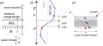
The photoinduced transient surface charge redistribution can appear in the sub-surface level (carrier separation, electronic excitation), at interfaces (charge transfer), and above the surface (photoemission), as exemplified in Fig. 1, and the magnitude of surface voltage () can be described generally from the sum of these components:
| (1) |
where z1 is the position at which the probing electron beam enters the field region and z0 is the position of the diffractively probed region. Effect of the these charge redistribution channels are categorized into respective photovoltages. Firstly, on the bulk level, the inner potential change IP resulted from the adjustment of valence electronic distribution can cause an abrupt refraction shift at the interface, whereas the adjustment/creation of a space charge region defines a transient voltage SC within the dielectric screening length. Secondly, on the surface level, the photoinduced interfacial charge transfer over a thin insulating barrier can create a dipole field region, which defines a voltage component DP on a nm length scale. Thirdly, photoemission can occur into the vacuum region, particularly for high intensity excitations. Subsequently a subsurface charge dynamics is induced to screen the field associated with photoelectron from penetrating into the bulk materials. Together, they create a near surface field imparting a potential difference PE on a time-dependent length-scale defined by the recovery of the photoelectrons to the surface. These four different mechanisms of surface voltage generation have characteristic time and length scales, their influences on the probing electron beam ultimately vary with incidence and exit angles and the interfacial structure. Generally, these photovoltages are linearly superposable, which allows them to be treated independently, and the overall surface voltage can be expressed as:
| (2) |
As a prototype example, photoinduced charge redistribution at Si/SiO2 interface (Fig. 1) is examined here, in which the voltammetry is contributed significantly from DP as the probing electron beam fully penetrate the top SiO2 layer, whereas it has only a short penetration depth ( 1 nm) into the Si underlayer. Since the screening length in semiconductor is relatively large( 1 m), the short penetration of the probing electron beam picks up only a small fraction of the voltage drop along the top SC region, whereas the surface dipole voltage across the SiO2 layer is fully sampled. Thus at a scenario where interfacial charge transfer occurs, DP can dominate over SC. Meanwhile, IP is generally small if phase transition is not involved. The contribution of PE is more difficult to assess. In the case of Si, the hot carriers are created with a high transient temperature, which can induce thermionic emission, and under an strong photofield from an intense laser irradiation the multiphoton photoemission is also possible,vanDriel2007 leading to a nonnegligible photoelectron contribution to the overall photovoltage. Nonetheless, due to the very different length scales involved in interfacial charge transfer and photoemission, we expect the dynamics to be rather different, which will be investigated with controlled experiments.
III Surface diffraction and rocking map characterization
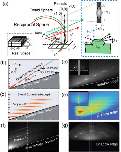
Since diffractive voltammetry employs diffracted beams, it is necessary to link the photo-induced distortion of diffraction pattern with the surface voltage generation. First, we examine the formalism of electron diffraction from different types of surface, which has been a source of confusion to properly understand the ultrafast surface electron diffraction process and a central topic to elucidate for deducing . Fig. 2(a) describes the production of the diffraction pattern from a grazing incident electron beam. The Ewald sphere is constructed to predict the diffraction pattern based on the intercept regions between the Ewald sphere and the reciprocal lattice network. This methodology is founded on a kinematic (Fourier) theory and can be extended to understand nanoscale diffraction, in which the size of the reciprocal lattice nodes, as depicted in the inset of Fig. 2(a), is determined by the persistent lengthPersistenceLengthNote of the lattice probed by the electrons. For a long-range-ordered smooth surface, the in-plane persistent length is very large (La in the inset of Fig. 2(a)) as compared to the penetration depth of the electron (Lc), producing very thin reciprocal rods (relrods). In the limit of Lc=0 (single layer), the reciprocal lattice becomes two-dimensional (2D) array of relrods, and the diffracted beam is defined by the intercept between the Ewald sphere and the relrod network, rendering circular diffraction patterns, generally described as the Laue zones in reflective high-energy electron diffraction(RHEED). For nanostructured surfaces, , so relrod widens significantly, and the diffraction pattern can deviate significantly from circular Laue patterns, and observing more than one diffraction peaks along a single relrod is possible.
To examine the relrod structure, we use rocking map characterization, which is conducted by rocking the sample plane against electron incidence, so Ewald sphere intercept rolls along the relrod. The rocking map is constructed by slicing a reflection stripe showing a relrod normal to the shadow edge in the diffraction image and stitching these stripes together as a function of incidence angle (). A diagonal line with slope (a) equal to 2 in the rocking map exposes the relrod structure in terms of vs. , as depicted in Fig. 2(b). The reciprocal node, which is a Fourier transform of a probed crystalline region defined by the persistence lengths of the samples as depicted in the inset of Fig. 2(a), can be examined from the out-of-phase to in-phase conditions in the rocking map. Near =0, the relrod structure is continuous. As increases the relrod becomes spotty, due to the increase of persistent length (Lc) with the increasing electron penetration depth as a function of . This trend is evidenced in an experimental rocking map produced from a relatively flat Si surface, as shown in Fig. 2(c). For the sake of clarity in discussion, we will refer to RHEED pattern only when dealing with a smooth surface that produces sharp circular Laue patterns, which is especially useful for monitoring the layer-by-layer growth in molecular beam epitaxy.AppLEED In so speaking, RHEED experiment is not well suited for studying structural dynamics study as neither does the position of the RHEED peak indicate the respective position of the reciprocal lattice node, nor does RHEED intensity directly inform lattice fluctuations, such as Debye Waller factor. Only through the inspection of the rocking map can the reciprocal lattice be exposed for structural investigation, nonetheless, such experiments are tedious to perform for dynamics study.RuanPNAS2004
Fortunately, more informative results can be obtained for nanostructured surfaces and interfaces where the diffraction mechanism differs from ‘RHEED’. In fact, typical ultrafast electron crystallography (UEC) studies,RuanScience2004 ; Baum2007 ; Gedik2007 ; Carbone2008 ; RamanPRL2008 rely on transmitted surface diffraction features produced with the grazing incidence electrons to determine structural dynamics. When the transverse persistent length ( in the inset of Fig. 2(a)) is short, such as steps and nanostructure-decorated surfaces, the widened relrods can extend several periods of the interferences (Bragg reflections), taking advantage of the high energy electron having a large Ewald sphere radius (90 at 30 keV) for extensive overlap with reciprocal lattice. As a result, the slope of the in-phase diffraction in the rocking map changes from 2 to 0, as it is now possible to penetrate the samples and produce transmission patterns. A simulated rocking map (Fig. 2(d)) shows this trend, which is verified by a study of highly oriented pyrolytic graphite (HOPG),RamanPRL2008 shown in Fig. 2(e). This type of features differ from ‘RHEED’ in that the transmitted diffraction spots carry the symmetry of the lattice and can be used for structural determination. With UEC operated in such circumstances, the intensity of transmitted Bragg peaks have been used to monitor the integrity of the lattice structure, including laser-induced thermal fluctuations and phase transition,RamanPRL2008 and have been exploited to investigate the surface-supported nanoparticles. NanoLetter2007 ; RamanPRL2011 What’s essential here for formulating the surface diffractive voltammetry is that the diffraction condition under has: , where is the electron wavelength, n is the diffraction order, and c is the lattice constant, can be used to formulate the diffracted beam trajectory under the presence of transient surface field, as described in Fig. 3. Details of the general formalism of UEDV for =0 or 2 under different surface diffraction conditions will be described in detail in Sec. IV. We also like to point out it is generally difficult to know the circumstances of surface diffraction without examining rocking map. For example, when employing resonance diffraction peaks appearing along a Kikuchi lineZLWang for UEDV, the surface diffraction must be characterized according to , as shown in Fig. 2(f)(map) and (g) (Kikuchi pattern). For this reason, it is central to identify the surface diffraction circumstance from the rocking map characterization before a proper interpretation of the data can be established.
IV The general formalism of electron diffractive voltammetry
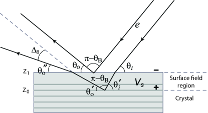
We derive the general formalism for describing the TSV-induced distortion of the diffraction pattern under different surface diffraction circumstances. We firstly generalize the problem in a simplified infinite long slab geometry, as depicted in Fig. 3, where a field region exists near the surface, caused by a photoinduced redistribution of charges. We consider the refraction effect separately for the incident and outgoing beams. As the electron beam enters the slab, the incidence angle is changed from into due to the refraction effect imposed by the surface field region. A similar refraction effect occurs as the diffracted beams cross the same region to reach the detector screen, which changes the exit angle from in the diffraction region to as the diffracted beam leaves the field region. The degree of change depends on the strength of field integrated along the incident and exit paths. Due to the grazing incidence geometry the change in is dominated by the field normal to the surface, we can relate the change in to based on momentum- energy relationship along z direction for the incoming beam:
| (3) |
where and are the momenta of the incident beam projected along at and . Expressed in terms of angle , Eq. (3) can be rewritten as:
| (4) |
where , by utilizing tan, tan, and is the beam energy prior entering the field region. Similarly for the outgoing beams, we have:
| (5) |
Since the electric field integration is linear, different components of the surface potential can be superposed on each other, thus the details of composition is not important here. The voltammetry is established when can be deduced as a function of the observable , which is defined as the angular shift of the diffracted beam (). The derivation of requires the knowledge of surface diffraction. To make the voltammetry generally applicable to different type of interfaces, we consider all scenarios discussed in Fig. 2 by relating and with
| (6) |
where is the slope along the in-phase diffracted beams in the rocking map. For example, belongs to the case of RHEED (Fig. 2(b)), is associated with the transmitted Bragg diffraction (Fig. 2(d)), and can be attributed to Kikuchi diffraction (Fig. 2(f)). Following the notation in Fig. 3, at the diffracted region:
| (7) |
which allows us to rewrite in Eq. (5), which we define as , in terms of and :
| (8) |
| (9) |
To get -induced angular shift in the diffraction pattern:
| (10) |
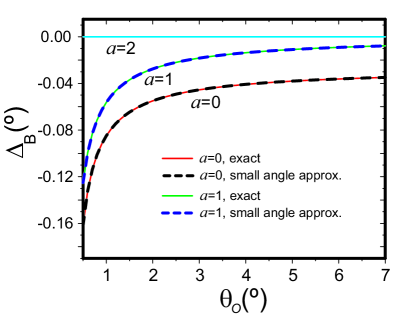
Since is a function of , it is difficult to deduce directly from Eq. (10). Small angle approximation allows inverting Eq. (10) to obtain for different , which is presented in the Appendix. One salient feature of the refraction-induced shift is that increases as decreases. This is easily seen in Fig. 4, where is calculated for at , following the exact solution based on Eq. (10). We note that the corresponding change in at is nearly twice the value at , whereas at , remains to be 0 for all . We also calculate using small angle solutions (Eqs. (27) & (30)) in the Appendix. The difference between the two is barely noticeable. These results show that voltammetry is best performed using nanostructured materials where the transmitted Bragg diffraction is possible (i.e. ), whereas UEDV would be impossible under strictly RHEED condition. Nonetheless, in real circumstances even for a relatively flat surface, is usually not exactly equal to 2, as shown in Fig. 2(c). Deviation from results in a small, but non-negligible sensitivity to . Generally, the angular dependence of -induced shift is opposite to the structure-related one, as the Fourier relationship: demands that if only the structural change is present would increase as increases. In contrast, the refraction-induced shift responds to oppositely, resulting in non-uniform cancellation of structure-induced shift. This nonreciprocal feature is the basis of a Fourier Phasing method,MM2008 used to correct the Vs-induced distortion in the diffraction pattern in order to accurately assess the structural dynamics.
V Ultrafast electron diffractive voltammetry experiment
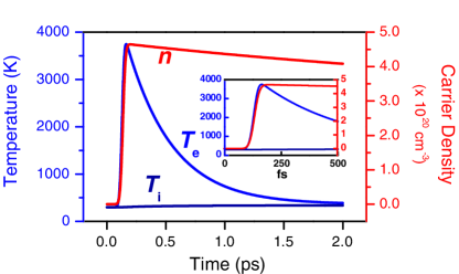
To demonstrate the methodology for UEDV, we conduct an experiment using a Si (111) substrate with a thin () insulating layer prepared via modified RCA cleaning.Kern1970 We employ a Ti:Sapphire laser (800nm) with photon energy of 1.55 eV, which is above the indirect bandgap (1.11 eV) of Si but below the bandgap of SiO2 (8.9 eV), to excite the carriers within the Si substrate. Using the Boltzmann transport coupled two-temperature model,MurdickThesis ; 9; Carpene2006 we can estimate the transient carrier density, and the quasi-equilibrium electronic and lattice temperatures in the electron probed region.MurdickThesis The coupling hierarchy for energy transduction is that the excitation photon first heats up the carriers through electronic relaxation in the sub-ps timescale, whereas the lattice temperature rises mainly through electron-phonon coupling on the ps timescale. In parallel, the energy transport takes place from excited surface into the bulk, driven by the temperature gradient, mediated by the carriers and the phonons. Because for Si the penetration depth () of the infrared laser is significantly longer ()Jellison1982 than that of the electron beam (, incident angle ), induction periods () for the temperatures to decay at the surface exist and can be estimated based on , where D is the diffusivity of the electrons and the phonons. We find that the the for electron ( 700 ps) is significantly longer than electron-phonon coupling time ( 5 ps), thus allowing the stored photon energy to be maintained within the photoexcited region to yield a lattice temperature rise on 5-10 ps timescale. Nonetheless, due to the long penetration depth and large disparity in the electronic and lattice heat capacities, even at a relatively high fluence of 65 , the lattice temperature rise is very small compared to that of the carriers having kinetic energy on par with the excitation energy, as revealed from the two-temperature model calculation shown in Fig. 5. The lattice temperature rises by only 40 K, yielding a thermal expansion of the lattice at most 0.011% (). In addition to the transient high temperature, the carrier concentration can increase by more than 3 orders of magnitude in the surface excited region from the intrinsic level,Chen2005 thereby creating a favorable condition for studying hot electron driven interfacial charge transfer across the layer.
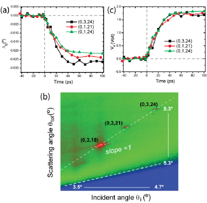
The signature of refraction-induced shift in the diffraction pattern lies in its angular dependence. We choose to investigate (0,3,24), (0,1,21), (0,1,24) on the (0,3) and (0,1) relrods with =7 and 8 (crystallographic notation for diffraction order is multiplied by a factor of 3 due to the ABC layering of the Si(111) surface), corresponding to of 6.24∘, 4.15∘, 4.70∘, and of 3.50∘, 4.02∘, 4.63∘ respectively. The excitation fluence is fixed at 65 mJ/cm2. Under photo-illumination, the transient movement of the three diffracted beams, depicted in Fig. 6(a), indeed exhibits nonreciprocal signatures as described previously, i.e. the higher order Bragg peak shifts less than the lower order one, which is characteristic of the TSV-induced effect.Murdick2008 Closer examination of the shifts shows that nonreciprocity applies only to , but not to , as the maximally shifted beam is (0,3,24), which has a =6.24∘ larger than the rest, whereas its corresponding is 3.50∘, which is smaller than the rest. This angular dependence is confirmed by the rocking map analysis for the relrods exhibiting near the in-phase diffraction, as shown in Fig. 6(b)) for (0,3) relrod. By applying in Eq. (10), we deduce for the three diffracted beams and render consistent TSV curves, independent of . Having established the validity of voltammetry measurement, we investigate the sources of the voltammetry in this study, which can be associated with suface/subsurface charge dynamics and/or photo-ionization creating photoelectrons.
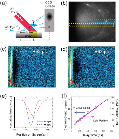
To isolate the contribution of free electrons produced by photo-ionization in the vacuum region, , we conduct a controlled study in which the photoelectron dynamics and the surface photovoltage are characterized simultaneously. This is achieved by using ultrafast electron shadow projection imaging approach, which has been reported previously for studying photoemission from an HOPG surface.RamanAPL2009 The advantage of electron projection imaging technique is that it can be implemented in situ with the voltammetry experiment by simply displacing the electron beam from the pump-probe overlap position by a distance () (Fig. 7(a)), thereby investigating the photoelectron dynamics under the same excitation condition as the voltammetry experiment. In addition, the diffracted beams, which are also visible in the shadow images, are affected only by photoemitted electrons above the surface generated by the pump laser, but not affected by the subsurface fields probed in the voltammetry geometry, thus establishing a clean way to evaluate the effect of in voltammetry.
In principle all the relevant information pertaining to photoemission for creating the transient near-surface field can be obtained by the projection imaging study. Fig. 7(c & d) show two selected snap-shots of the shadow images of the photoemitted electron cloud obtained at t=42ps and 62ps under a laser fluence of 65 . The initial lateral dimension of the electron cloud is determined by our pump laser incident at to the surface normal. As a result, the laser footprint is elliptical with and , which are determined by the cross-correlation response by scanning the probe beam across the laser illuminated region.MM2008 The projection distance (source-to-camera) employed in this study is 16.5 cm, and the offset distance , giving a magnification factor . The linescan of the shadow images (integrated vertically along the yellow stripe depicted in Fig. 7(b)) contains the respective temporal evolvement of Gaussian-like electron cloud together with a near-surface build-up (lines colored in red in Fig. 7(c & d), and from fitting the linescansRamanAPL2009 (Fig. 7(e)) at different times the temporal evolution of cloud width () and center-of-mass position () can be determined, as depicted in Fig. 7(f) for . From these temporal profile changes, we observe a linear increase of position and width, and extract an electron cloud expansion velocity and an initial CoM velocity .
The creation of shadow images can be understood based on scattering of the probing electrons from the collective field established by the photoelectrons:
| (11) |
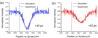
The deflection from the collective field reduces the numbers of originally forward-going electrons reaching the CCD camera, thus effectively creating a shadow of the electron cloud. This process can be directly simulated by an N-particle simulationTao2012 employing Monte Carlo sampling of a 3D Gaussian electron distribution, which is parameterized based on s obtained from fitting the shadow images. We then send rays of electrons representing the probing electron beam across the 3D electron cloud whose collective field is calculated first by summing the pair-wise fields from individual electrons within the cloud. To speed up the calculation, we establish a mean-field model to match the results calculated from on the multi-particle calculation based on the impact parameter to the electron cloud.Tao2012 We note that the deflection caused by the collective field is linear with respect to the electron density in the regime of interest here, which warrants the usefulness of the mean-field approach. To simulate the shadow formation, electron rays are used along the line of sight to establish the shadow line scans and the electron counts on the CCD screen are calculated with and without intervening by the 3D electron cloud. The shadow profiles are constructed by dividing the electron counts along the line scans with the rays being intersected by the 3D could in the path and the line scans without intersection and compared with the experimental results. Fig. 8 shows the comparison at two different delay times at t=42 and 62 ps (solid lines are N-particle simulation results and dashed lines are the fitted gaussian profiles obtained from experimental shadow images). The agreement between the N-particle simulations and the shadow imaging results are excellent. Since here the depth of the shadow is proportional to the photoemitted electron density, the agreement of between the experiment and simulation not only indicates the robustness of the shadow imaging technique in profiling the photoemission, but also offering a measurement of the photoelectron density created by the photo-illumination.
An independent approach to deduce the photo-electron density is through a single-beam deflection experiment across the photo-emitted electron cloud.ParkAPL2009 Importantly, the 3D cloud geometry established by the shadow imaging technique can be confirmed by the deflection of a diffracted beam from Si(111) surface diffraction, as it traverse through the collective field associated with photoelectrons. Single-beam deflection experiment has the advantage of being highly sensitive to the field and so is applicable even at very long times (ns) when the electron cloud become very diffusive to monitor by the shadow imaging approach. To extend the field characterization to longer time, we analyze the Si-111 beam deflection data contained in the diffraction images obtained from shadow imaging experiment. The analysis is on a Kikuchi diffraction enhanced peak (with =2.01∘ & =5.76∘) along the central stripe region circled by the dashed line in cyan in Fig. 7(b)). Fig. 9(a) shows the temporal evolution of the angular shift. The up and down swings of the beam can be associated with the beam crossing from above and under the 3D electron cloud.ParkAPL2009 Importantly, the electron density required in correctly simulating the shadow profile can now be directly confirmed by simulating the specific electron trajectory using an N-particle calculation as described earlier. Furthermore, the absolute downward shift of the diffracted beam is also affected by the counter image force associated with the image charges that are created on the surface responding to the photoemission, which is also modeled numerically as described below.
VI Near surface field induced by photoemission
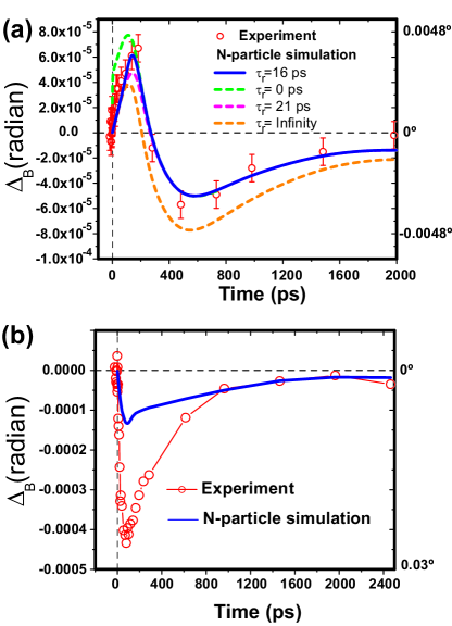
To fully simulate the diffracted beam deflection trajectory, which extends to 2 ns, we need to know the projectile motion of the 3D electron cloud and the corresponding image charge dynamics that provide additional field component. To comply with the rate and the magnitude of beam deflection, a metal-like dielectric response with a very large at early times due to the excessive amount of charges initially built up on surface is considered. decays exponentially to the equilibrium value of 3.9 for SiO2,MeyerBook and can be described by =3.9 + A . The field model for image charges is included with the dielectric relaxation process and is described by:JacksonBook
| (12) |
The time-dependent angular shift of diffracted beam is calculated using:
| (13) |
where =30kV and E in the path integral contains contributions from photoelectrons (Eq. (11)) and image charges (Eq. (12)). The integration takes place over 3FWHM across the Gaussian cloud. Previously, an analytical modelParkAPL2009 and N-particle simulationZewailAPL2010 of the transient field associated with photoelectron cloud and image charges have been implemented to account for deflection of a probing electron beam. The dielectric response of the surface has not been exclusively included. The necessity in incorporating the surface dielectric relaxation to account for the change in is evident from comparing the models with different dielectric relaxation times and the experimental data, which are shown in Fig. 9(a). We find A= and =16 ps provide a reasonable agreement to the experimental data. To comply with the deflection data at long times, the knowledge of the photoelectron cloud beyond the initial linear trajectory is needed. The return rate of the photoelectrons to the surface is determined by the strength of the image force, which is gradually weakened as the expansion of the photoelectron cloud into the surface will lead to cancellation of the image charges even before the CoM trajectory reaches the turning point and weakens the image force. We apply an additional 3rd order term to account for this effect. The deflection of the diffracted beam can be calculated self-consistently by varying the coefficients of the 2nd and 3rd order polynomials to fit the deflection data. We note that the fitting is based on a fixed initial condition (electron density and CoM and expansion velocity) determined by shadow imaging, but the results from fitting deflection data extend our knowledge of the surface field development beyond the timescale (0-150 ps) obtainable from the shadow imaging, and serve as the basis for estimating the long time behavior for the voltammetry measurement.
VII Surface photovoltage
Having obtained the near surface field associated with the photoelectrons from the shadow imaging and diffracted beam deflection measurements in the offset geometry, we can now evaluate the contribution associated with photoemission in the voltammetry experiment conducted by shifting the beam from the offset geometry to the overlap geometry, as reported in Fig. 9(b) (line and symbols, colored in red). The diffracted beam used in the voltammetry experiment appears at the intercept of a Kikuchi line and a 2D reciprocal lattice rod (Fig. 2(g)). We characterize the diffraction being a two-step process, where the incident beam is first scattered randomly to form an isotropic source, and then scattered into surface Laue Zones. This is consistent with observed in the vs relationship obtained from the rocking map analysis presented in Fig. 2(f), implying that only the refraction along the exit path contributes to , and so we can simplify the generalized TSV formula accordingly, and deduce the photovoltage based on: (see Appendix, Eq. (31)).
We evaluate the contribution PE in the overall photovoltage measurement by building on the knowledge of near surface fields induced by photo-emission characterized by the shadow imaging and deflection experiments. The associated with PE can be calculated by an N particle simulation of along the exit beam path at , similar to that in evaluating the deflection experiment, but under an overlap geometry used in the voltammetry experiment. Thus-simulated is depicted in Fig. 9(b) (solid line, colored in blue) to represent the PE contribution, and compared to the overall measured experimentally. Remarkably, the photoemission-associated matches very well with the long-time tail of the voltammetry measurement, but contributes maximally about 25-30% of the total angular shift at the early times. This indicates that the slow dynamics of TSV at the long time are controlled by the return of the photoemitted electrons to the surface, whereas interfacial charge transfer across the SiO2 layer is more relevant at the short times. By excluding the PE contribution from the overall , we deduce a Vs(t) relevant to the surface charging dynamics, as depicted in Fig. 10.
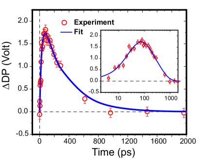
By fitting the PE subtracted Vs(t) with an effective RC-charging/discharging model:
| (14) |
we determine RC time constants: =30.84 ps, and =296.47 ps respectively for surface charging and discharging. We attribute the difference between the two to the change of hot electron photoconductivity across the SiO2 interface. The photo-generated hot electrons facilitate the surface charging through access to the excited states, leading to a much shorter RC time than the discharging, which involves a cooler interface with a reduced photoconductivity, leaving the SiO2 surface to stay charged for a longer period of time. Surface charging processes have previously also been investigated by electric field induced second harmonic generation (EFISH), LEE1967 ; CHEN1983 ; MIHAYCHUK1995 ; Aktsipetrov1996 ; Dadap1997 ; Baldelli2000 in which the sub-surface electric field is deduced based on modeling the field-enhancement of optical second harmonic generation signal as well as photoemission.Marsi2000 We find that the field strength 1-5 V/nm, obtained in our study of the Si/SiO2 interface, is very similar to what was found in EFISH studies under similar excitation conditions,Aktsipetrov1996 ; Dadap1997 but because of a lower laser repetition rate is applied here (1 kHz in UEDV, compared to 80 MHz in EFISH), cyclic residual charge accumulation from deep trap statesMihaychuk1999 ; Scheidt2008 ; Jun2004a ; Tolk2007 is avoided, allowing the transient charging behavior to be resolved directly.
We compare the TSV results reported here for a smooth Si/SiO2 interface with one reported previously for a step Si/SiO2 interface. We find that the timescales in charging and discharging the interface in the two studies are similar, whereas the TSV induced in the smooth interface (maximum 1.7V at 65 mJ/cm2) is smaller than the stepped interface (maximum 3V at 72 mJ/cm2). By applying the shadow imaging technique under the same conditions (electron incidence/exit angles and laser fluences) as the voltammetry experiment, we are able to quantitatively identify the contribution of photoemission on the overall voltammetry result, where photoemission is mainly responsible for the slow decay, but does not contribute significantly to the short time dynamics, which clarifies the origin of the diffracted beam movement.ParkAPL2009 For cases where photoexcitation can cause significant structural changes, a correction on the refraction-induced shift in diffraction pattern is needed. We point to the first ultrafast electron crystallography investigation of Si(111) surface, which was performed using 266 nm laser pulse.RuanPNAS2004 Because of the much shorter laser penetration depth (4nm), the absorbed optical density is concentrated near the surface, propelling not only hot electron dynamics, but also surface structural changes. From examining the reported time-dependent rocking curve (Fig.4(a) in the paperRuanPNAS2004 ), the movement of the ‘in-phase’ Bragg peak at small angle () is slightly larger than that of a peak at higher angle(), which is consistent with a surface refraction phenomenon being present. But the surface charging is not the full story, as the ‘surface’ structural dynamics was also examined in the ‘out-of-phase’ condition(Fig.4(b) in the paperRuanPNAS2004 ), where the presence of multiple interference peaks is a signature of transmitted diffraction from surface nanostructure. Such a pattern was modeled using a slab model that identified the changes are from the top surface layer and the sub-surface (111) layers, contributing the contrasting movements of the two different peaks separated in . The surface dynamics could be mediated by the impulsive strain induced by ultrafast laser pulse heating and/or surface charges. Further controlled study is needed to clarify the nature of the surface dynamics on surface charging, photo-emission and the corresponding structural dynamics, which can be achieved using the methodologies provided here(see discussion in Sect. VIII.4).
VIII Diffractive Voltammetry beyond slab model
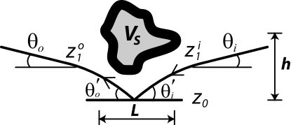
While the general formalism deduced in Sec. IV is limited to a smooth interface in which the transient surface field is modeled to have a slab geometry, the basic concept of diffractive voltammetry is applicable to different types of interfaces beyond the slab geometry. For different geometries, the timescales of the charge redistribution can likely be deduced correctly from (t), whereas Vs(t) deduced using the slab-formalism is merely an effective parameter for TSV, which is subjective to corrections from the shape factor and the boundary conditions affecting the field integration at the nanointerface. To treat TSV beyond an infinite slab model, we extend the TSV formalism described in Eq. (10) to consider refraction shift with finite size and non-planar geometries. Under such circumstances, the location of in Eq. (1) needs not to be the same for incident and diffracted electron beams, and the effective that the electron beam experiences can be accounted for by applying the finite-size correction factors, and to separately describe the deviation of electron trajectory from the infinite slab model. This generalized picture, in which we can parameterize the finite interface structure with a nominal lateral length and vertical height with an aspect ratio parameter , is depicted in Fig. 11. The corresponding and associated with the interface can be obtained numerically by ray tracing methods.
| (15) |
| (16) |
and
| (17) |
where
| (18) |
Here, . Applying small angle approximation allows the voltammetry formalism: to be established analytically, which is detailed in the Appendix. Below we give two examples to show how the correction terms can be implemented for dealing with more complex nanostructured interfaces beyond the infinite slab model.
VIII.1 Correction for a finite slab geometry
The simplest extension of an infinite slab formalism is to consider the edge effects in a finite slab geometry. Using aspect ratio , where and are the height and width of the slab, as the probing electron beam enter and exit from the sides, the apparent voltage observed by the electron beams is reduced from , which can be approximated by the correction factor:
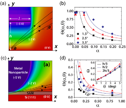
| (19) |
To assess the validity of this approximation, we perform an electron ray tracing simulation FieldPrecision with a setup shown in Fig. 12(a) to calculate , which accounts for the fringe fields not included in Eq. (19). We calculate a few instances of as a function of and show that the analytical expression described in Eq. (19) is a fairly good approximation for , as illustrated in Fig. 12(b). The finite-slab correction effectively suppresses the divergence of as the diffracted electron beam approaches the shadow edge ( approaches 0).
VIII.2 Correction for a spherical nanoparticle decorated interface
A frequently encountered molecular electronic interface involves replacing the top piece of the finite slab with a spherical nanoparticle, and has a molecular contact between the nanoparticle and the substrate. In order to model the TSV in this spherical interface, the correction factor is parameterized as a function of angle (). Ray tracing, as depicted in Fig. 12(c), shows that the (Fig. 12(d)) determined for this spherical interface is amazingly similar to that of the flat finite slab interface (Fig. 12(b)), if we re-define , where is the diameter of the nanoparticle and is the thickness of the molecular contact layer. For small angle diffraction (), the dispersion in due to position-dependent refraction effect can be ignored, as shown in the inset of Fig. 12(d), calculated for the 20 nm nanoparticle interface.
VIII.3 Charge transport in substrate-molecule-nanoparticle interface
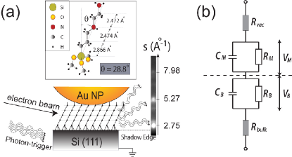
The transient electron diffractive approach can be used to investigate silicon-molecule-gold nanoparticle interface, a prototypical system employed to study electron transport in molecaulr contacts.Bezryadin1997 ; Tian1998 ; Aswal2006 ; Chen1999 ; Forrest2004 This experimental scheme is shown in Fig. 13(a), where a self-assembled monolayer (SAM) is built on the hydroxylated Si substrate through silanization as the molecular contact, and covered by 20 nm gold nanoparticlesAswal2006 ; NanoLetter2007 . The transient charging of the nanoparticle, caused by photoinduced charge transfer between the substrate and the nanoparticle through SAM, establishes a voltage determined by the charging energy of the nanoparticles w.r.t. the driving surface potential and the resistance of SAM, which can be conceptualized as an effective RC circuit as depicted in Fig. 13(b). The diffracted beams from SAM layer, order =1 to 3, at = 2.75, 5.27, 7.98 as shown in Fig. 13(a), are employed to investigate the charge transfer dynamics between the nanoparticles and the substrate. The capacitance can be calculated directly from the geometry of the interface using a finite element method.FieldPrecision When C is known, the resistance of the SAM can be directly deduced by the RC time in the charging and discharging of the nanoparticle/SAM/Si interface. Due to that the interfacial molecular diffraction is also deflected by the imposing surface potential rise from the substrate, obtained from the overall of the molecular diffraction consists of , the voltage across the SAM, and , which encompasses the surface charging and photoemission potential background.
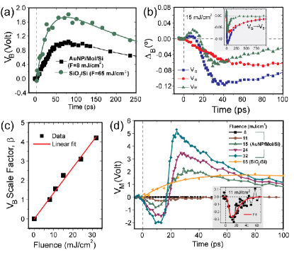
We first investigate by examining the low fleunce data (F 10 mJ/cm2) where the driving force is insufficient to overcome the molecular potential barrier to charge up the nanoparticles. The voltammetry performed at F=8 mJ/cm2 indeed shows a very similar transient to that obtained from bare SiO2/Si interface (Fig. 10). Comparison of the low fluence voltammetry result with that of SiO2/Si is shown in Fig. 14(a), verifying that the low fluence is solely from the surface charging potential of the Si surface, denoted here as (8 mJ/cm2). Increasing fluence beyond 10 mJ/cm2 produces structures on the 10 ps timescale over the smooth , showing first upward swing and then downward swing, exemplified in the subtracted , or , as exemplified in Fig. 14(b) for F=15 mJ/cm2, which are characteristic of molecular charge transport. We write
| (20) |
, where is the voltage across the SAM. Here, the superposition principle is applied to s in Eq. (20), which is true when (see Appendix for discussion). Since is driven by hot carriers in the nanoparticles and the Si substrate, should approaches 0 at a long time, or in other words, as t . We verify this by scaling up the (F=8 mJ/cm2) to higher fluences according to (F)=(F=8 mJ/cm2) to compare and at long times, where is expect to be . Indeed, the long time transient of matches nearly perfectly with that of at F=15 mJ/cm2, as shown in the inset of Fig. 14(b). We verify this for all the data at higher fluences. The values of obtained from comparing and are reported in Fig. 14(c), which shows a nearly linear relationship between and F, as expected.
With being well characterized, we are now poised to examine the photo-induced transport properties associated with SAM. Fig. 14(d) shows under different fluences. The is deduced first calculating (), according to Eq. (20), and then converting () to by applying Eq. (34), in which =-0.0958 & =-0.0234, calculated according to =1.4∘ & =0.44∘ in our probing geometry. Examination of fluence-dependent (t) reveals the following novel features compared to the surface charging dynamics of SiO2/Si interface (also shown in Fig. 14(d) for comparison):
(1) The photovoltage sampled by SAM-diffracted beam is ‘negative’ at first, indicating a net positive charge on the gold nanoparticles following photoemission. This shows that the initial photo-induced process is electron transfer from nanoparticles to Si surface. Since neither the carrier concentration nor the carrier temperature can be increased significantly for metallic nanoparticles by photoexcitation, as compared to Si substrate, the early electron migration to Si surface might suggest a laser-induced surface plasmon effect being present, excited in the gold nanoparticles that promotes a surface-field assisted or multi-photon internal ionization for nanoparticle charging.RamanPRL2011
(2) A ‘reverse’ charging process occurs as the fluence is increased beyond 11 mJ/cm2, as evidenced in the surging of after 10 ps at F=15 mJ/cm2, which reaches a positive value at 22 ps. The reversal of nanoparticle charging is driven by the overcharging of Si surface. The reversal time is short, within 5 ps at high fluence. The rapid reversal is indicative of a field-induced dielectric breakdown in SAM, which becomes a conductor as the interfacial field reaches a threshold value ( 0.8 V/nm according to Fig. 14(d)). Following the breakdown, the relaxation of the stored electrons in the nanoparticles is much slower ( 40 ps), indicating a recovery of the dielectric constant to the insulator status in SAM.
(3) The charging and reverse charging in nanoparticles are apparently not equal. The positive maximum (electron charging) is approximately twice as large as the negative maximum (hole charging) in Fig.14(d). This asymmetry in photoconductivity could be intrinsic to SAM, or it could be associated with the probing geometry in which the electron beam is more effectively deflected by Si surface than by nanoparticles due to a curved interface. In the latter case, the difference in maximum on the two polarities might not be associated with the difference in the stored charges within the nanoparticles. Further numerical evaluation of the asymmetry in the probing geometry is needed to clarify.
It is rather interesting to compare the molecular resistance deduced from this ultrafast voltammetry measurement with the steady-state resistance data,Sato1997 obtained by applying a bias voltage across the molecular interface, reporting an of 12.5 M using 10 nm (thus a SAM area 4 times smaller) Au nanoparticle. We determine the nominal molecular resistance by obtaining the RC time constants from fitting (t) recorded at F=11 mJ/cm2, which is beneath the dielectric breakdown threshold. The fit using Eq. (14), depicted in the inset of Fig. 14(d), shows a nearly equal and of 81 ps. Based on the effective RC model, we obtain a resistance 2.74 M using =2.9210-18 Farad, deduced from finite element modeling of the interface. The obtained using ultrafast voltammetry is 4 times smaller than the steady-state measurement for 10 nm particle, which shows the molecular resistivity obtained from two different methods are nearly identical.
VIII.4 Diffractive voltammetry and ultrafast electron diffraction
Evidenced from the general presence of photovoltage in photoexcited nanostructures, especially under intense laser excitation, in order to quantitatively determine the structural evolution, the refraction-induced shift in the diffraction pattern needs to be accounted for. Fortunately, because of the ‘non-reciprocal’ nature of the refraction shift, a self-consistent correction scheme can be implemented by applying a counter shift based on TSV-formalism to the diffraction spectrum. The correction aims to re-establish the Fourier relationship between the structure and diffraction pattern through iterative forward and backward Fourier transforms,RamanThesis ; MM2008 which is termed Fourier Phasing (FP) scheme. The pre-requisite of an effective FP is that a sufficiently wide range of Fourier space encompassing several Bragg peaks is available for extract Fourier components, i.e. the pair-correlation function.MM2008 This FP scheme has been successfully applied to extract the pair-correlation function for surface-supported nanoparticlesMM2008 and graphite.RamanPRL2008 It has been shown that so long as a large portion of the Bragg spectrum is corrected, the structural changes, especially deduced based on the nearest neighbor distances, is robust, and the effective used to parameterize the refraction-shift can ne deduced reliably. Nonetheless, the absolute magnitude of TSV is subject to whether an exact TSV formalism has been identified, which is determined by the geometry and the surface diffraction condition. This robustness arises from the inverse trend of the refraction shift in contrast to the structure-related shift and partially from the similarity between diffraction TSV formalisms, as discussed in this paper.
IX Summary
We have established a general formalism for ultrafast electron diffractive voltammetry concept, which is applied to investigate the photoinduced charge migration from the substrate to nanostructured interfaces. We show that the surface diffraction and boundary condition need to be accounted for correctly formulating the ultrafast voltammetry based on Coulomb refraction-induced diffracted beam dynamics. We identify that the voltammetry appears on the surface, subsurface, and vacuum levels, associated with interfacial charge transfer, carrier diffusion, and photoemission respectively, under intense laser irradiation. From quantitative shadow imaging techniques performed at the same condition as voltammetry and N-particle simulations, we are able to assess the voltammetry contribution associated with photoemission, and quantitatively deduce the surface charging dynamics from the overall voltammetry. We find that the photoemission impacts the voltammetry most in the long time, whereas the interfacial charge dynamics dominates the voltammetry on the ultrafast (0-100 ps) timescale. Miraculously, we are able to extend the diffractive voltammetry methodology to investigate molecular charge transport process under a strong field induced by laser at a gold nanopaticle/molecule/Silicon interface. At low field circumstance, we obtain similar molecular resistivity as the steady-state measurement, whereas at high fields we observe a molecular dielectric breakdown resembling a field-induced insulator-to-metal transition. The spurious photoemission effect can be suppressed by using a low energy or less intense laser pulse as the high-energy tail of the excited spectrum can be largely cut off under these conditions. The future applications of this methodology lie in more definitive, site-selected voltammetry studies on nanostructured and heterogeneous interfaces, which can be enabled by the development of nanometer scale high-brightness ultrafast electron beam system for ultrafast electron microscope, which already starts to take shape.ZewailScience2010 ; Kim2008 ; Tao2012
X Acknowledgment
We acknowledge R. Worhatch, R.K. Raman, Y. Murooka for earlier contribution to nanoparticle work, and valuable exchanges with A.H. Zewail, J.C.H. Spence, and J.M. Zuo. This work is supported under grant DE-FG02-06ER46309 from the Department of Energy. Partial support for R.A. Murdick is under grant 45982-G10 from the Petroleum Research Fund of the American Chemical Society.
Appendix A Formalism of diffracted voltammetry under small angle condition
A.1 Slab model
UEDV formalism can simplified by applying small angle approximation: & , and . Under these conditions, Eq. (8) is reduced to:
| (21) |
Also, is modified as
| (22) |
By combining Eq. (21) & Eq. (22), we can get the following equation:
| (23) |
Solving Eq. (23) for , we arrive at the following relationship:
| (24) |
where
| (25) |
| (26) |
Simplification can be made for different value. For , Eq. (23) can be simplified as:
| (27) |
so the inversion can be made analytically:
| (28) |
which is equivalent to Eq. (1) in the previous study.Murdick2008
If & , Eq. (28) can be further linearized:
| (29) |
If & ,
| (32) |
For , implying in RHEED geometry, we can reduce the general formalism to
| (33) |
Therefore, the surface scattered diffraction change, , is independent of . In other words, the measured in experiments is not affected by TSV.
A.2 Beyond slab model
References
- (1) D.M. Adams, L. Brus, C.E.D. Chidsey, S. Creager, C. Creutz, C.R. Kagan, P.V. Kamat, M. Lieberman, S. Lindsay, R.A. Marcus, et al., J. Phys. Chem. B 107 (2003) 6668.
- (2) M. Gratzel, J. Photochem. Photobiol. C - Photochem. Rev. 4 (2003) 145.
- (3) A. Aviram and M.A. Ratner, Chem. Phys. Lett. 29 (1974) 277.
- (4) P. Avouris, Z. Chen, and V. Perebeinos, Nat. Nanotechnol. 2 (2007) 605.
- (5) A. Bezryadin, C. Dekker, and G. Schmid, Appl. Phys. Lett. 71 (1997) 1273.
- (6) M. Haruta, Catal. Today 36 (1997) 153.
- (7) R. Marcus, N.Sutin,Biochim. Biophys. Acta811 (1985)265.
- (8) C.J. Chen, Introduction to Scanning Tunneling Microscopy (Oxford University Press, 1993).
- (9) S. Datta, Electronic Transport in Mescoscopic Systems(Cambridge University Press, 1995).
- (10) G. Ashkenasy, D. Cahen, R. Cohen, A. Shanzer, A. Vilan, Accounts Chem. Res. 35 (2002) 121.
- (11) J. Hu, T. Odom, C. Lieber, Accounts Chem. Res. 32 (1999) 435.
- (12) A. Alivisatos, Science 271 (1996) 933.
- (13) J. Kong, N. Franklin, C. Zhou, M. Chapline, S. Peng, K. Cho, H. Dai, Science 287 (2000) 622.
- (14) A.Shipway, E. Katz, I. Willner, ChemPhysChem 1 (2000) 18.
- (15) A. Kongkanand, K. Tvrdy, K. Takechi, M. Kuno, P.V. Kamat,J. Am. Chem. Soc. 130 (2008) 4007.
- (16) K.S. Leschkies, R. Divakar, J. Basu, E. Enache-Pommer, J.E. Boercker, C.B. Carter, U.R. Kortshagen, D.J. Norris, E.S.Aydil, Nano Lett. 7 (2007) 1793.
- (17) J.M. Luther, M. Law, M.C. Beard, Q. Song, M.O. Reese, R.J. Ellingson, A.J. Nozik, Nano Lett. 8 (2008) 3488.
- (18) S. Schmitt-Rink, D.A.B. Miller, D.S. Chemla, Phys. Rev. B 35 (1987) 8113.
- (19) H. Benisty, C.M.Sotomayor-Torres, C. Weisbuch, Phys. Rev. B 44 (1991) 10945.
- (20) N. Anderson, T. Lian, Annu. Rev. Phys. Chem. 56 (2005) 491.
- (21) R.J.D. Miller, G.L. McLendon, A.J. Nozik, W. Schmickler, and F. Willig, Surface Electron Transfer Processes (VCH Publishers, Inc., New York, 1995).
- (22) A. Kubo, K. Onda, H. Petek et al., Nano Letter 5 (2005) 1123.
- (23) W. Fuss, W.E. Schmid, S.A. Trushin, J. Chem. Phys. 112 (2000) 8347.
- (24) J.G. Mihaychuk, N. Shamir, H.M. van Driel, Phys. Rev. B 59 (1999) 2164.
- (25) I. Robel V. Subramanian, M. Kuno, P. Kamat, J. Am. Chem. Soc. 128 (2006) 2385.
- (26) W. Tian, S. Datta, S. Hong, R. Reifenberger, J. Henderson, C. Kubiak, J. Chem. Phys. 109 (1998) 2874.
- (27) D. Aswal, S. Lenfant, D. Guerin, J. Yakhmi, D. Vuillaume, Anal. Chim. Acta 568 (2006) 84.
- (28) J. Chen, M. Reed, A. Rawlett J. Tour, Science 286 (1999) 1550.
- (29) O. Dulub, M. Batzill, S. Solovev, E. Loginova, A. Alchagirov, T.E. Madey, U. Diebold, Science 317 (2007) 1052.
- (30) J.A. Misewich, T.F. Heinz D.M. Newns, Phys. Rev. Lett. 68 (1992) 3737.
- (31) M.A. Henderson, W.S. Epling, C.H.F. Peden, C.L. Perkins, J. Phys. Chem. B 107 (2003) 534.
- (32) Y. Miyamoto, Appl. Phys. Lett. 91 (2007) 113120.
- (33) Ramani K. Raman, Yoshie Murooka, Chong-Yu Ruan, Teng Yang, Savas Berber, David Tomnek, Phys. Rev. Lett. 101 (2008) 077401.
- (34) Ryan A. Murdick, Ramani K. Raman, Yoshie Murooka, Chong-Yu Ruan, Phys. Rev. B 77 (2008) 245329.
- (35) S. Sch fera, W. Lianga, A. H. Zewail, Chem. Phys. Lett. 493 (2010) 11.
- (36) D. Saldin, J.C.H. Spence, Ultramicroscopy55 (1994) 397.
- (37) N. Yamamoto, J.C.H. Spence, Thin Solid Films104 (1983) 43.
- (38) J.C.H. Spence, H.Poon, D.Saldin, Microsc. Microanal.10 (2004) 128.
- (39) The shift in diffraction due to electron wavlength change in the materials, which is on the level of per 1 volt in photovoltage for 30 keV electron beam, is small compared to refraction shift, which is on the level under the same condition.
- (40) Ryan A. Murdick, Ph.D. thesis, Michigan State University, East Lansing (2009).
- (41) S. Paul, N. Rotenberg, H.M. van Driel, Appl. Phys. Lett. 93 (2008) 131102.
- (42) The persistence length here refers to the length of the crystal in the sample that allow the probing electron to scatter coherently to form diffraction pattern. The persistence length can be limted by the size of the crystal, the coherence length of the probing electron, or the pentration depth of the probing electron, which ever is the smallest.
- (43) W. Braun, Applied RHEED. Reflection high energy electron diffraction during crystal growth (Springer, Berlin, 1999).
- (44) C-Y. Ruan, F. Vigliotti, V.A. Lobastov, S. Chen, A.H. Zewail, Proc. Natl. Acad. Sxi. USA 101 (2004) 1123.
- (45) C-Y. Ruan, V.A. Lobastov, F. Vigliotti, S. Chen, A.H. Zewail, Science 304 (2004) 5667.
- (46) P. Baum, D.-S. Yang, A.H. Zewail, Science 318 (2007) 788.
- (47) N. Gedik, D.-S. Yang, G. Logvenov, I. Bozovic, A.H. Zewail,Science 316(2007) 425.
- (48) F. Carbone, P. Baum, P. Rudolf, A.H. Zewail, Phys. Rev. Lett. 100 (2008) 035501.
- (49) C-Y. Ruan, Y. Murooka, R.K. Raman, R.A. Murdick, Nano Lett. 7 (2007) 1290.
- (50) R.K. Raman, R.A. Murdick, R.J. Worhatch, Y. Murooka, S.D. Mahanti, T-R. T. Han, and C-Y. Ruan, Phys. Rev. Lett. 104 (2010) 123401.
- (51) Z.L. Wang, Reflection electron microscopy and spectroscopy for surface analysis (Cambridge University Press, New York, 1996).
- (52) C-Y. Ruan, Y. Murooka, R.K. Raman, R.A. Murdick, Microscopy and Microanalysis 15 (2009) 323.
- (53) W. Kern, D.A. Poutinen, RCA Rev. 31 (1970) 187.
- (54) J.K. Chen, D.Y. Tzou, J.E. Beraun, Int. J. Heat Mass Transf. 48 (2005) 501.
- (55) E. Carpene, Phys. Rev. B 74 (2006) 024301.
- (56) G.E. Jellison, F.A. Modine, Appl. Phys. Lett. 41 (1982) 180.
- (57) R.K. Raman, Z. Tao, T-R. Han, C-Y. Ruan, Appl. Phys. Lett. 95 (2009) 181108 .
- (58) Z. Tao, C-Y. Ruan, Unpublished.
- (59) H. Park and J. M. Zuo, Appl. Phys. Lett. 94 (2009) 251103.
- (60) P.R. Gray, P.J. Hurst, S.H. Lewis, R.G. Meyer, Analysis and Design of Analog Integrated Circuits, Fifth ed. (Wiely, New York, 2009).
- (61) J.D. Jackson, Classical Electrodynamics, 3rd ed., (Wiely, New York, 1998).
- (62) C.H. Lee, R.K. Chang, N. Bloembergen, Phys. Rev. Lett. 18 (1967) 167.
- (63) C.K. Chen, T.F. Heinz, D. Ricard, Y.R. Shen, Phys. Rev. B 27 (1983) 1965.
- (64) J.G. Mihaychuk, J. Bloch, Y. Liu, H.M. van Driel, Opt. Lett. 20 (1995) 2063.
- (65) O.A. Aktsipetrov, A.A. Fedyanin, E.D. Mishina, A.N. Rubtsov, C.W. vanHasselt, M.A.C. Devillers,T. Rasing, Phys. Rev. B 54 (1996) 1825.
- (66) J.I. Dadap, Z. Xu, X.F. Hu, M.C. Downer, N.M. Russell, J.G. Ekerdt, O.A. Aktsipetrov, Phys. Rev. B 56 (1997) 13367.
- (67) S. Baldelli, A. Eppler, E. Anderson, Y. Shen, G. Somorjai, J. Chem. Phys. 113 (2000) 5432.
- (68) M. Marsi, R.Belkhou, C.Grupp, G. Panaccione, A.Taleb-Ibrahimi, L.Nahon, D. Garzella, D. Nutarelli, E. Renault, R. Roux et al., Phys. Rev. B 61 (2000) R5070.
- (69) J.G. Mihaychuk, N. Shamir, H.M. van Driel, Phys. Rev. B 59 (1999) 2164.
- (70) T. Scheidt, E.G. Rohwer, P. Neethling, H.M. von Bergmann, H. Stafast, J. Appl. Phys. 104 (2008) 083712.
- (71) B. Jun, R. Schrimpf, D. Fleetwood, Y. White, R. Pasternak, S. Rashkeev, F. Brunier, N. Bresson, M. Fouillat, S. Cristoloveanu et al., IEEE Trans. Nucl. Sci. 51 (2004) 3231.
- (72) N.H. Tolk, M.L. Alles, R. Pasternak, X. Lu, R.D. Schrimpf, D.M. Fleetwood, R.P. Dolan, R.W. Standley, Microelectron. Eng. 84 (2007) 2089.
- (73) The electrostatics calculations were performed using the Charged Particle Toolkit software from Field Precision. The geometry was setup according to Fig.12(a & c). In both cases, a potential of Vs=-5 V was imposed. For nanoparticle simulations, the relative permittivity of the dielectric layer was set to 2.5. The Si(111) was treated as a grounded metal because of the high carrier density under photoexcitation. The potential far away from the nanoparticle was set to 0. Electrons of 30 keV were initialized at different launch angles (1∘ to 5∘) and positions along the height of the dielectric layer (1/3, 1/2, and 2/3). The slab model calculations were also carried out with this software, with varying capacitor slab separations.
- (74) S. Forrest, Nature 428 (2004) 911.
- (75) T. Sato, H. Ahmed, D. Brown, B. Johnson, J. Appl. Phys. 82 (1997) 696.
- (76) R.K. Raman, Ph.D. thesis, Michigan State University, East Lansing (2010).
- (77) A.H. Zewail, Science 328 (2010) 187.
- (78) J.S. Kim, T. LaGrange, B.W. Reed, M.L. Taheri, M.R. Armstrong, W.E. King, N.D. Browning, G.H. Campbell, Science 321 (2008) 1472.
- (79) Z. Tao, H. Zhang, P.M. Duxbury, M. Berz, C.-Y. Ruan, J. Appl. Phys. 111 (2012) 044316.