The electronic transport of top subband and disordered sea in InAs nanowire in presence of a mobile gate.
Abstract
We performed measurements at helium temperatures of the electronic transport in an InAs quantum wire ( k) in the presence of a charged tip of an atomic force microscope serving as a mobile gate. The period and the amplitude of the observed quasiperiodic oscillations are investigated in detail as a function of electron concentration in the linear and non-linear regime. We demonstrate the influence of the tip-to-sample distance on the ability to locally affect the top subband electrons as well as the electrons in the disordered sea. Furthermore, we introduce a new method of detection of the subband occupation in an InAs wire, which allows us to evaluate the number of the electrons in the conductive band of the wire.
pacs:
73.23.Hk, 73.40.Gk, 73.63.NmI Introduction
In the past decade an increasing number of investigations were dedicated to the electronic transport in semiconductor nanowires Li2006 ; Thelander2006 ; Appenzeller2008 ; Yang2010 . Especially nanowires based on III-V semiconductors, e.g. InAs, are very attractive as conductive channels in devices for nano-electronic applications Bryllert2006 ; Dayeh2007 . Apart from more application-driven investigations, InAs nanowires are also very suitable objects to study fundamental quantum phenomena, i.e. single electron tunneling Fasth2005 ; Shorubalko2007 or electron interference Dhara2009 ; Roulleau2010 ; Hernandez2010 ; Bloemers2011 , at low temperatures. At helium temperatures the transport in InAs nanowires is mostly diffusive and typical values of the elastic mean free path are of the order of a few tenth of nanometers Dhara2009 ; Roulleau2010 ; Bloemers2011 . Information on electron phase coherence can be extracted from the temperature dependence of universal conductance fluctuations Hernandez2010 ; Bloemers2011 .
In order to gain detailed information of local conductance features in low-dimensional systems, mobile gate measurements employing a charged AFM tip (scanning gate microscopy measurements or SGM measurements) have been established as a standard method. Quantum point contacts TopinkaS2000 ; TopinkaN2001 ; SchnezQPC2011 , quantum rings Hackens2006 , quantum dots based on heterojunctions Pioda2004 ; Gildemeister2007 ; Huefner2011 , graphene Schnez2010 , and carbon nanotubes Bockrat2001 ; Woodside2002 ; Zhukov2009 have been investigated comprehensively using SGM. Investigations of local electronic transport in InAs nanowires with scanning gate microscopy were performed at room temperature Zhukov2011E ; Zhou2007 as well as at He temperatures Bleszynski2005 ; Boyd2011a ; Zhukov2011 ; Zhukov2012 ; Zhukov2012P ; Zhukov2013 . However, these studies mostly focused on wires with initially existing Bleszynski2005 ; Zhukov2011 ; Zhukov2012 ; Zhukov2013 or artificially created Boyd2011a defects, i.e. potential barriers made of InP, which divided the nanowire into series of quantum dots.
Recently, in InAs nanowires without defects with characteristic resistance values of 30 k unexpected quasi-periodic oscillations of the resistance along the wire were observed in SGM scans Zhukov2012P . The non-monotonic dependence of the period of the observed oscillations on the back-gate voltage allowed to associate them with electrons in the top subband with a small Fermi wavelength comparable with the length of the wire () altering the resistance of the whole system. These electrons do not scatter on the surface of the nanowire and do not mix with other free electrons of the lower laying mixed subbands (disordered sea). However, the experiment reported in Ref. Zhukov2012P left the mechanism behind the oscillations as an open question.
Here, we present a detailed investigation of the resistance oscillations in an InAs nanowire, namely the tracing of the oscillation from a clearly defined two-nodes state through a three-nodes one to a state where minima split. Furthermore the stability of two-nodes oscillations in the non-linear regime is discussed. We demonstrate the influence of the tip-to-sample distance on a ability to locally influence the top subband electrons as well as the electrons in the disordered sea. We suggest a new method to determine the occupation of the topmost subband using a line trace of a charged AFM tip along the wire. This method allows us to evaluate the number of conductive electrons added to the InAs wire on applying a positive back-gate voltage.
II Experimental
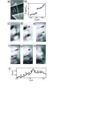
In our experiment we study a nominally undoped InAs nanowire grown by selective-area metal-organic vapor-phase epitaxy Akabori2009 . The diameter of the wire is 100 nm. The wire was placed on an -type doped Si (100) substrate covered by a 100 nm thick SiO2 insulating layer. The Si substrate served as the back-gate electrode. The evaporated Ti/Au contacts to the wire as well as the markers of the search pattern were defined by electron-beam lithography. The distance between the contacts is m. A scanning electron beam micrograph of the sample is shown in Fig. 1a). The source and drain metallic electrodes connected to the wire are marked by S and D .
All measurements were performed at K. The charged tip of a home-built scanning probe microscope AFM is used as a mobile gate during scanning gate imaging measurements. All scanning gate measurements are performed by keeping the potential of the scanning probe microscope tip () as well as the back-gate voltage () constant. The conductance of the wire during the scan is measured in a two-terminal circuit by using a standard lock-in technique. Here, a driving AC current with an amplitude of nA at a frequency of 231 Hz is applied while the voltage is measured by a differential amplifier. Two typical tip to SiO2 surface distances were chosen for the scanning process nm, i.e. the tip is far from the surface and nm, i.e. the tip is close to the surface.
III Experimental results
In Figs. 1c) to h) scanning gate microscopy images in the linear regime are shown which are obtained at back-gate voltages of , 9.14, 9.50, 9.62, 9.94 and 10.40 V, respectively, keeping the tip voltage fixed at zero. The tip-to-surface distance during these measurements was kept at nm. Increasing the back-gate voltage the situation develops through a well-defined two-nodes pattern [cf. Figs. 1c) and d)], then passing a two-to-three nodes regime [cf. Figs. 1e) and f)] and subsequently to a well-defined three-nodes one [cf. Fig. 1g)]. The corresponding positions of nodes in the SGM scans are marked by pink and blue triangles for two-nodes and three-nodes patterns, respectively. At and 9.94 V in the single resonance regime [cf. Figs. 1c) and g)] the oscillations are well-defined, while in the intermediate regime the oscillations are slightly less visible [cf. Figs. 1e) and f)]. Finally, at the highest back-gate voltage of 10.40 V, the pattern evolves into a four-nodes regime with split minima, as can be inferred from Fig. 1h). A crosscut of this pattern along the wire axis is shown in Fig. 1i). The resulting eight quasi-periodic minima are marked by down-nose triangles.
In order to access the rigidity of the observed oscillations we calculated the ratio , with the effective wire length and the distance between the nodes. As can be seen in Fig. 1b), the ratio defined above strongly depends on the back-gate voltage and resembles a staircase shape with well developed plateaus. In order to adjust the position of the lower step to an integer node number , we used a value of m for the effective wire length . This value is slightly smaller than the geometrical length of the wire m but looks reasonable keeping in mind the presence of the depletion regions at the interfaces between the wire and the metallic contacts.
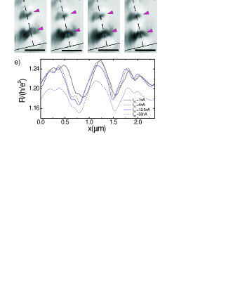
Next we present scanning gate measurements, where the driving current through the nanowire was increased stepwise. The images shown in Figs. 2a) to d) correspond to a , 4, 12.5 and 50 nA, respectively. These measurements were obtained by applying a back-gate voltage of V and setting to zero. Once again the tip is kept far from the surface ( nm). It is worth noting that while in Figs. 2a) to c) the energy corresponding to the typical source-to-drain voltage is smaller than the thermal energy , while for the case of Fig. 2d) the situation is opposite i.e. meV, with is the Boltzmann constant. Crosscuts of Figs. 2a) to d) along wire axis are shown in Fig. 2e). As can be seen here, no significant deviations of the node positions and the amplitude of the oscillations are found up to nA. However, a slight suppression of the oscillations and a decrease of the resistance are observed in the strong non-linear regime at nA.
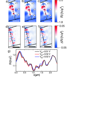
For the next two sets of SGM images shown in Figs. 3a) to f) a closer tip-to-surface distance of nm was chosen. These measurements were performed in the linear regime by using a driving current of 1 nA. The first set, shown in Figs. 3a) to c), is measured at smaller back-gate voltages of , 3.98 and 3.99 V The triangles mark the nodes of three-nodes pattern created by conductive electrons of the top subband. The second set of scans depicted Figs. 3d) to f) is taken at higher back-gate voltage of 8.51, 8.52 and 8.53 V, respectively. Here, the smooth background was subtracted, in order to emphasize the small scale ripples on the scan. As a reference, Fig. 3g) shows crosscuts along the wire axis of pristine SGM data (without subtraction) at the different back gate voltages.
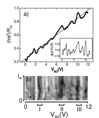
The next set of experimental data is dedicated to resistance vs. back-gate dependencies for different charged tip positions. Once again, for all measurements the tip voltage is set to zero. First, in Fig. 4a) the dependence of the normalized reciprocal wire resistance , i.e. the normalized conductance, on the back-gate voltage is shown, where the tip is placed a a fixed location far from the wire. The location of the spot is indicated by a in Fig. 1a). The trace shown in Fig. 4a) will serve as a reference for the later position dependent measurements. The fluctuating conductance can be assigned to the phenomena of universal conductance fluctuations Altshuler1985b ; Lee1987 . The corresponding fluctuation amplitude can be determined by first subtracting the background conductance obtained from a linear fit of . The remaining fluctuations are shown in the inset of the Fig. 4a). Here, a typical value of fluctuation amplitude of for the back-gate voltage range of V. This value fits well to comparable measurements on InAs nanowires Hernandez2010 ; Bloemers2011 .
Next we will present a set of measurements, where the tip is placed equidistantly from source to drain at fixed positions along the dashed line indicated in Fig. 1a). In Fig. 4b) the deviation of the conductance with respect to the conductance with a tip positions far from the wire is plotted as a function of back-gate voltage for the different positions . Three well defined minima in the conductivity (grooves) are observed around , 7.5 and 10.5 V marked by I, II and III in Fig. 4b).
IV Discussion
In our previous work SGM experimental data with 10, 2, 3 and 4 standing wave nodes () have been presented Zhukov2012P . These experimental results were obtained in the previously mentioned resonance condition . While the nodes are the most pronounced features, no information about in between resonances were provided. It was found in Ref. Zhukov2012P , that the oscillation amplitude drops as is increasing, thus the transformation from to was chosen in the present study as the preferable range to extract in out of resonance condition. The observed staircase shape dependence of vs. , as indicated in Fig. 1b), is qualitatively in good agreement with the model of standing waves of ballistic electrons in the top transverse quantization subband. Standing waves are the result of the presence of potential barriers at metal-semiconductor interfaces. In the models of Wigner crystallization of Luttinger liquid and Friedel oscillations a similar dependence of vs. is expected Ziani2012 . It is worth noting that the barrier at the top wire to contact interface is more pronounced according to SGM pictures, so standing wave appears to be “pinned” to the top contact, i.e. the top contact to node distance increases as increases.
One finds, that the kinetic energy eV is essentially less than even for the three-nodes resonant state. Here, is the effective mass of electron in InAs, is the free electron mass, is the Planck constant. In addition, the thermal length nm is considerably smaller than the length of the wire m. The energy difference between the two-nodes and three-nodes resonance states is less than because both states are resolved simultaneously at a back-gate voltage V [cf. Fig. 1f)]. The Coulomb energy of the electron-electron interaction, , even for the three-nodes resonant state is less than as well. Here, is the static dielectric constant in InAs, nm is the distance from the center of the wire to the doped back-gate, and is the vacuum permittivity. Thus, the ability of Wigner crystallization, Friedel oscillations and standing wave scenarios looks rather doubtful for and 3. The Coulomb interaction between electrons becomes comparable to the temperature meV only at V when the average distance between the electrons is around 250 nm. We may speculate that the formation of a Wigner crystal in the top subband happens at this back-gate voltage with a to transformation of the oscillations.
Nevertheless, the experimentally observed resistance oscillations are apparently connected to the formation of charge density modulations in the top subband. Besides this, the mechanism of the effect of the charge density oscillations on the resistance of the whole wire is more due to the tip-induced spatial fluctuations of the chemical potential of the top subband Ziani2012 ; Gindikin2007 ; Soeffing2009 . Additionally, some suppression of the conductance of the disordered sea due to the increasing charge density in the top subband in the node location similar to Tans ; Zhukov2011E is expected. Thus two mechanisms alter the resistance of the whole wire in opposite direction.
SGM images presented in Fig. 2 demonstrate the robustness of the two-nodes resonant state to application of source to drain voltage. As it was mentioned above, no significant deviations of the node positions and the amplitude of the oscillations are found as long as . Only the application of a large current of nA resulting in meV suppresses the oscillations and decreases the resistance [cf. Fig. 2e)].
The results of the SGM scans made when the tip to surface distance is 220 nm, i.e. the closest distance from tip to the wire axis is of 170 nm, are presented in Figs. 3a) to g). As previously stated, if the distance from the tip to the wire axis the density oscillations of the top sublevel are probed while at the charged tip disturbs the disordered sea as well. The characteristic deviation of the back-gate voltage inducing the redistribution of conductivity maxima and minima in SGM images when tip is scanning over the nanowire () is about 10 mV. In contrast to that, the width of the step in dependence of is more than hundred millivolts. The irregular pattern observed in SGM scans governed by the disordered sea has the smallest typical length scale of 200 nm, this is in accordance with expected spatial resolution of the experimental set up for mn. The amplitude of the deviations of resistance [cf. Fig. 3g)] is comparable with the amplitude of the universal conductance fluctuations shown in Fig. 4a) (inset).
In Ref. Zhukov2012P the abrupt increasing of the was interpret as the formation of the new subband in the InAs wire. Just at the instance the subband formation electrons are loaded simultaneously to the disordered sea and to the band with increasing of the back-gate voltage. Electrons loaded to the new subband are blocked because of the potential barriers at the wire to contact interfaces forming a semi-opened quantum dot. This dot decreases the total conductance of the wire at certain range of back-gate voltage, namely from of quantum dot formation to the value of the back-gate voltage when the barriers become transparent. Lets call the center of this range . It is possible to slightly alter with the charged AFM tip. Taking into account that electrons in quantum dot are concentrated in the center of the wire, as a function of the tip position along the wire must have one maximum Zhukov2009 ; Boyd2011 . This maximum is traced by the dashed line in Fig. 4b). Thus, three subbands are formed marked as I, II and III in the region of back-gate voltage of 0 V V at , 7.5 and 10.5 V, respectively. There is some discrepancy for back-gate voltages less than 1 V in the determination of the formation of the second subband comparing to the data in Ref. Zhukov2012P , where the formation was determined directly from SGI scans. It originates from the hysteresis in of the sample.
The formation of three subbands in the 0 V V back-gate region means that the number of free electrons loaded into wire is less than 100, while the total amount of electrons added to wire calculated from the capacitance is around 2000 Zhukov2012P . It means that most of the electrons in the wire are trapped probably because of interface states charged by changing the back-gate voltage. This also means that the value of mean free path must be recalculated as well. It seems is actually larger than the typically used value of 40 nm even for disordered sea. We would like to remind that a value of nm was measured by Zhou et al. Zhou at room temperature.
V Conclusion
We performed measurements at helium temperatures of the electronic transport in an InAs nanowire (k) in the presence of a charged tip of an atomic force microscope serving as a mobile gate. The period and the amplitude of previously observed quasi-periodic oscillations are investigated in detail as a function of back-gate voltage in the linear and non-linear regime. None of the scenario such as Friedel oscillations, Wigner crystallization or standing wave looks applicable to explain the origin of observed oscillations at and 3. We demonstrate the influence of the tip-to-sample distance on an ability to influence locally the top subband electrons as well as the electrons in the disordered sea. We suggest a new method of evaluation of the number of conductive electrons in an InAs wire. This method results in the conclusion that most of the electrons added to nanowire conductive band on applying a positive back-gate voltage are trapped.
VI Acknowledgments
This work is supported by the Russian Foundation for Basic Research, programs of the Russian Academy of Science, the Program for Support of Leading Scientific Schools, and by the International Bureau of the German Federal Ministry of Education and Research within the project RUS 09/052.
References
- (1) Yat Li, Fang Qian, Jie Xiang, and Charles M. Lieber. Nanowire electronics and optoelectronic devices. Materials Today, 9:18, 2006.
- (2) C. Thelander, P. Agarwal, S. Brongersma, J. Eymery, L.F. Feiner, A. Forchel, M. Scheffler, W. Riess, B.J. Ohlsson, U. Gösele, and L. Samuelson. Nanowire-based one-dimensional electronics. Materials Today, 9:28–35, 2006.
- (3) J. Appenzeller, J. Knoch, M. T. Björk, H. Riel, H. Schmid, and W. Riess. Toward nanowire electronics. Electron Devices, IEEE Transactions on, 55(11):2827–2845, 2008.
- (4) Peidong Yang, Ruoxue Yan, and Melissa Fardy. Semiconductor nanowire: What s next? Nano Letters, 10(5):1529–1536, 2010.
- (5) T. Bryllert, L.-E. Wernersson, T. Lowgren, and L. Samuelson. Vertical wrap-gated nanowire transistors. Nanotechnology, 17:227, 2006.
- (6) Shadi A. Dayeh, David P. R. Aplin, Xiaotian Zhou, Paul K. L. Yu, Edward T. Yu, and Deli Wang. High electron mobility InAs nanowire field-effect transistors. Small, 3:326–332, 2007.
- (7) C. Fasth, A. Fuhrer, M. T. Bjork, and L. Samuelson. Tunable double quantum dots in inas nanowires defined by local gate electrodes. Nanoletters, 5:1487–1490, 2005.
- (8) I Shorubalko, A Pfund, R Leturcq, M T Borgström, F Gramm, E Müller, E Gini, and K Ensslin. Tunable few-electron quantum dots in InAs nanowires. Nanotechnology, 18(4):044014, 2007.
- (9) P. Roulleau, T. Choi, S. Riedi, T. Heinzel, I. Shorubalko, T. Ihn, and K. Ensslin, Phys. Rev. B 81, 155449 (2010).
- (10) S. Dhara, H.S. Solanki, V. Singh, A. Narayanan, P. Chaudhari, M. Gokhale, A. Bhattacharya, and M.M. Deshmukh, Phys. Rev. B 79, 121311(R) (2009).
- (11) C. Blömers, M.I. Lepsa, M. Luysberg, D. Grützmacher, H. Lüth, and Th. Schäpers, Nano Lett. 11, 3550 (2011).
- (12) S. Estévez Hernández, M. Akabori, K. Sladek, Ch. Volk, S. Alagha, H. Hardtdegen, M.G. Pala, N. Demarina, D. Grützmacher, and Th. Schäpers, Phys. Rev. B 82, 235303 (2010).
- (13) A.C. Ford, J.C. Ho, Yu-L. Chueh, Yu-Ch. Tseng, Zh. Fan, J. Guo, J. Bokor and A. Javey, Nano Lett. 9, 360 (2009).
- (14) S.A. Dayeh, Semicond. Sci. Technol. 25, 024004 (2010).
- (15) S. Wirths, K. Weis, A. Winden, K. Sladek, C.Volk, S. Alagha, T. E. Weirich, M. von der Ahe, H. Hardtdegen, H. Lüth, N. Demarina, D. Grützmacher, Th. Schäpers, J. Appl. Phys., 110 053709 (2011).
- (16) M.A. Topinka, B.J. LeRoy, S.E.J. Shaw, E.J. Heller, R.M. Westervelt, K.D. Maranowski, A.C. Gossard, Science 289, 2323 (2000).
- (17) M.A. Topinka, B.J. LeRoy, R.M. Westervelt, S.E.J. Shaw, R. Fleischmann, E.J. Heller, K.D. Maranowski and A.C. Gossard, Nature 410, 183 (2001).
- (18) S. Schnez, C. Rössler, T. Ihn, K. Ensslin, C. Reichl, and W. Wegscheider, Phys. Rev. B 84, 195322 (2011).
- (19) B. Hackens, F. Martins, T. Ouisse, H. Sellier, S. Bollaert, X. Wallart, A. Cappy, J. Chevrier, V. Bayot and S. Huant, Nature Phys. 2, 826 (2006).
- (20) A. Pioda, S. Kicin, T. Ihn, M. Sigrist, A. Fuhrer, K. Ensslin, A. Weichselbaum, S.E. Ulloa, M. Reinwald, and W. Wegscheider, Phys. Rev. Lett. 93, 216801 (2004).
- (21) A.E. Gildemeister, T. Ihn, M. Sigrist, K. Ensslin, D.C. Driscoll, and A.C. Gossard, Phys. Rev. B 75, 195338 (2007).
- (22) M. Huefner, B. Kueng, S. Schnez, K. Ensslin, T. Ihn, M. Reinwald, and M. Reinwald, Phys. Rev. B 83, 235326 (2011).
- (23) S. Schnez, J. Güttinger, M. Huefner, Ch. Stampfer, K. Ensslin, and Th. Ihn, Phys. Rev. B 82, 165445 (2010).
- (24) M. Bockrat, W. Liang, D. Bozovic, J.H. Hafner, Ch.M. Lieber, M. Tinkham, H. Park, Science 291, 283 (2001).
- (25) M.T. Woodside and P.L. McEuen, Science 296, 1098 (2002).
- (26) A.A. Zhukov and G. Finkelstein, JETP Lett. 89, 212 (2009).
- (27) A.A. Zhukov, Ch. Volk, A. Winden, H. Hardtdegen and Th. Schäpers, Physica E 44, 690 (2011).
- (28) X. Zhou, S.A. Dayeh, D. Wang, E.T. Yu, J. Vac. Sci. Technol. B 25, 1427 (2007).
- (29) A.C. Bleszynski, F.A. Zwanenburg, R.M. Westervelt, A.L. Roest, E.P.A.M. Bakkers, and L.P. Kouwenhoven, Nano Lett. 7, 2559 (2005).
- (30) A.A. Zhukov, Ch. Volk, A. Winden, H. Hardtdegen and Th. Schäpers, JETP Lett. 93, 13 (2011).
- (31) A.A. Zhukov, Ch. Volk, A. Winden, H. Hardtdegen and Th. Schäpers, ZhETF 142, 1212 (2012).
- (32) A.A. Zhukov, Ch. Volk, A. Winden, H. Hardtdegen and Th. Schäpers, ZhETF 143, 158 (2013).
- (33) E.E. Boyd, K. Storm, L. Samuelson and R.M. Westervelt, Nanotechnology 22, 185201 (2011).
- (34) A.A. Zhukov, Ch. Volk, A. Winden, H. Hardtdegen and Th. Schäpers, JETP Lett. 96, 109 (2012).
- (35) M. Akabori, K. Sladek, H. Hardtdegen, Th. Schäpers, and D. Grützmacher, J. Cryst. Growth 311, 3813 (2009).
- (36) A.A. Zhukov, Instrum. Exp. Tech. 51, 130 (2008).
- (37) B. Al’tshuler, Pis’ma Zh. Eksp. Teo. Fiz. [JETP Lett. 41, 648-651 (1985)] 41, 530 (1985).
- (38) P. A.Lee,A. D.Stone, and H. Fukuyama, Phys. Rev. B 35, 1039 (1987).
- (39) N.T. Ziani, F. Cavaliere, and M. Sassetti, Phys. Rev. B 86, 125451 (2012).
- (40) Y. Gindikin and V.A. Sablikov, Phys. Rev. B 76, 045122 (2007).
- (41) S.A. Söffing, M. Bortz, I. Schneider, A. Struck, M. Fleischhauer, and S. Eggert, Phys. Rev. B 79, 195114 (2009).
- (42) S.J. Tans, C. Dekker, Nature 404, 834 (2000).
- (43) E.E. Boyd, R.M. Westervelt, Phys. Rev. B 84, 205308 (2011).
- (44) X. Zhou, S.A. Dayeh, D. Aplin, D. Wang, and E.T. Yu, Appl. Phys. Lett. 89, 053113 (2006).