All optical Amplification in Metallic Subwavelength Linear Waveguides
Abstract
Proposed all optical amplification scenario is based on the properties of light propagation in two coupled subwavelength metallic slab waveguides where for particular choice of waveguide parameters two propagating (symmetric) and non-propagating (antisymmetric) eigenmodes coexist. For such a setup incident beams realize boundary conditions for forming a stationary state as a superposition of mentioned eigenmodes. It is shown both analytically and numerically that amplification rate in this completely linear mechanism diverges for small signal values.
pacs:
42.81.Qb, 42.79.Ta, 42.60.DaLeading ideas in investigations of all optical logical devices in structured media christo usually implement optical bistability bi ; ramaz or soliton interaction mcleod in creating switching operation of optical beams. Quantum dots dot , single molecule mol or atomic systems atom could be also used for optically controlled switching of light. One can also quote various optoelectronic approaches opto for realization of optical transistors and asymmetric nonlinear waveguides for all optical diodes lepri . However, all the mentioned setups are based on nonlinear photon-photon interactions and hardly meet the criteria photo for applicability in all optical computing. Here we consider the possibility of amplification of optical signals using two subwavelength waveguides coupled by metallic film. The problem is linear with no need in high power fields and there is a reach experience in building of subwavelength photonic segev and metallic waveguides metal .
Our idea of all optical amplification is based on the possibility of coexistence of two fundamental modes with real (symmetric mode) and imaginary (antisymmetric mode) wavenumbers along longitudinal propagation direction of dielectric-metal-dielectric combined waveguide system. In such a situation only symmetric mode can carry nonzero flux, while the energy flux associated with antisymmetric mode is exactly zero. Thus the propagation of antisymmetric mode responsible for destructive interference is suppressed and amplification effect can take place.
Suggested effect is different than one in a homodyne receiver scheme, where signal intensity is amplified at the receiver area, while the total signal energy flux is not amplified. As we will show below, the total signal flux amplification is possible only in metallic subwavelength waveguides, where symmetric and antisymmetric modes are characterized by real and imaginary wavenumbers, respectively.
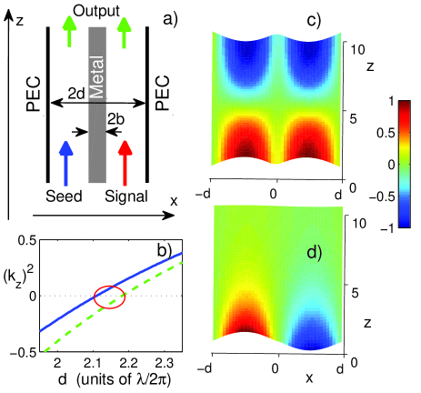
In principle, proposed waveguide system could be of different geometries, in this paper we just consider two dielectric slabs (with refractive index ) separated by metallic film and we assume perfect electric conductor (PEC) condition at both sides of waveguide system. Thus the setup presented in Fig. 1a just allows to reduce the problem to 2 (space) + 1 (time) dimensions assuming the electric field polarized and homogeneous along direction and having fixed zero value at the boundaries. In nonmagnetic medium we can write down the following wave equations for the transverse electric field perpendicular to plane:
| (1) |
where we work in the units and a definition is introduced. First equation in (1) corresponds to the wave propagation in a dielectric, while the second describes dynamics inside metallic film in approximation of zero Drude relaxation rate. Beyond this approximation electromagnetic wave dynamics inside metal is governed by ash
| (2) |
where stands for the electric current density, stands for Drude relaxation rate, is a plasma frequency; , and are charge, concentration and mass of electrons, respectively.
For the sake of analytical simplifications we assume negligible damping inside the metal () getting from (2) automatically the initial system (1), and we will work in nontransparent for the metal frequency range . Moreover, because of the placement of PEC at both sides of the waveguide system, one has vanishing boundary conditions . Thus stationary basic solution of (1) in the different parts of the combined dielectric-metal-dielectric symmetric waveguide system is written as follows:
| (3) | |||
where ”c.c.” means complex conjugated term. Here we assume that in the combined part of the waveguide one has a dielectric in the range and metal in the range ; , , and are real amplitudes of electric field in dielectric and metallic parts, respectively, is a real wavenumber in the dielectric, is a working frequency and is penetration depth in the metal. These wavenumbers are linked by the dispersion relations
| (4) |
which automatically follows putting solution (3) into wave equations (1). Fixing operational frequency and waveguide parameters and , all other quantities are uniquely defined. Particularly, from the continuity conditions of solution (3) at the lines one gets following relations for :
| (5) |
where we have () sign for symmetric (antisymmetric) solution. Taking into account dispersion relations (4) one can calculate and versus waveguide parameters and and we are interested in the range of these parameters for which is positive while is negative (see Fig. 1b for the appropriate parameter values indicated by a circle). Then defining real quantities as and we can write for symmetric and antisymmetric solutions:
| (6) |
where orthogonal to each other symmetric and antisymmetric profiles are defined as:
| (7) | |||
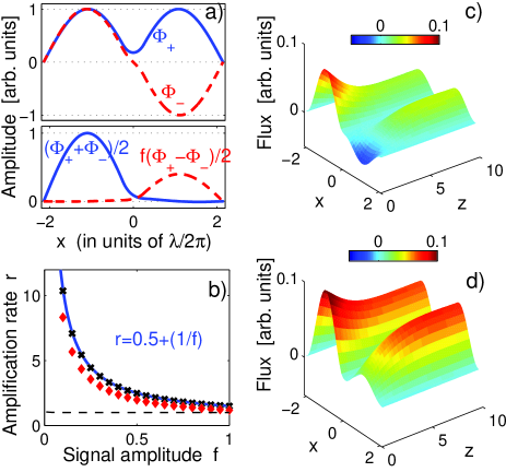
and we present snapshots of symmetric and antisymmetric solutions (6) in Fig. 1c,d while their profiles (7) along axis and their combinations are presented in Fig. 2a.
As far as electric field has a single component along transversal axis one can readily compute in-plane components of magnetic field, particularly, could be easily integrated form the Maxwell equation . Then it is straightforward to calculate energy flux density as and total energy flux along longitudinal direction . It is easy to see from (6) and (7) that averaged over time total flux in case of symmetric eigenfunction is , while in antisymmetric case one has a standing wave profile along direction and consequently averaged total flux is exactly zero.
Now the question is which solution (symmetric or antisymmetric one or their linear combination) is realized for the given boundary condition. Let us suppose that seed and input beams are injected from the isolated waveguides separated by perfect electric conductor (PEC). Thus we have the seed and input waveguides bounded by PEC at and , respectively, and first of all we consider symmetric incident field in the form of the following propagating wave at :
| (8) |
This should be combined with the reflected beam with unknown amplitudes and characterizing symmetric and antisymmetric contributions
| (9) |
and the sum should be connected with the linear combination of the solutions at given by Exp. (6) via continuity conditions. Noting that in case of narrow metallic films (see Fig. 2a) and we easily get the condition , meaning that there is no reflected wave and in a whole range of and the symmetric solution is approximately given by:
| (10) |
While in case of antisymmetric incident field the analysis is a bit more complicated, particularly, if we take the incident field in the form
| (11) |
from the similar to above continuity considerations we conclude that such a beam is completely reflected and a whole solution is written as follows:
| (12) |
for and , respectively, and the costants are defined as and .
Now let us suppose that we have an incident seed beam entering into the left waveguide and this could be presented as a linear combination of symmetric (8) and antisymmetric (11) incidences:
| (13) |
and as a consequence a whole solution under such a boundary conditions is given as linear combination of complete solutions (10) and (12) (see also bottom panel of Fig. 2a):
| (14) |
From (13) it is easy to calculate total averaged in time flux carried by seed beam entering into the left waveguide: . At the same time, calculating the energy flux of the complete solution and taking into account that the flux of antisymmetric solution is strictly zero, one gets half of the value of incident averaged flux: , meaning that only half of the incident intensity goes through the waveguide system and the rest is reflected back. As we will show below, by injecting signal beam (having the same phase as the seed beam) into the right waveguide reflected flux gradually decreases increasing amplitude of the signal beam and reaches zero value when both input and seed beam have equal amplitudes. This is a reason for amplification mechanism of the signal beam. For quantitative description of this effect we perform the similar analysis for the incident signal field with amplitude , particularly, presenting it as
| (15) |
This incident field carries the averaged total flux
| (16) |
which is a total gain of incident flux due to application of the signal field. Thus in case of application of both seed (13) and signal (15) beams the total incidence is and it realizes the complete solution in the form:
| (17) |
From the similar to above arguments that antisymmetric mode is characterized by a zero averaged flux, it is obvious that such a solution carries the averaged flux and thus total gain of the output flux due to the signal is read as
| (18) |
and this should be compared with averaged over time input signal flux (16), and thus one gets for the amplification rate:
| (19) |
which diverges at small signal values.
It should be especially emphasized that such amplification of signal beam takes place only in case of subwavelength waveguides when the wavenumber of antisymmetric solution takes imaginary value. In case of non-subwavelenth waveguides both symmetric and antisymmetric solutions are characterized by real wavenumbers which have very close values. Defining real wavenumber of antisymmetric mode as we note that antisymmetric mode is also characterized by nonzero flux, and from (17) now we get a following expression for the amplification rate:
| (20) |
For instance, if one has twice wider waveguide system the coefficient at the divergent term is negligible making amplification mechanism ineffective: (see dashed line in Fig. 2b).
Next our aim is to confirm this analytical result by numerical simulations. For this purpose we should first derive the boundary-value data at the lines and ( is a length of the system) following Ref. chen ; jerome , that represent incident waves entering the combined waveguide from the seed and signal and going out. As we have mentioned above before entering the waveguide system the seed and signal fields are described by Exps. (13) and (15), thus in the range the solution reads
| (21) |
where one has for
| (22) |
for and , respectively, while is unknown amplitude profile for reflected wave and has thus to be eliminated. The continuity conditions at with the electric field inside the combined waveguide can be written as
which can be combined to exclude the unknown reflected amplitude taking time derivative from the first equation and then combine resulting one with the second equation. The similar manipulations could be done with boundary conditions at but now there is no contribution of backward propagating field, thus the resulting equations read as
| (23) |
Thus we solve numerically initial equations (1) with boundary conditions (23) and definition (22) for . Next we compute averaged over time longitudinal flux density inside the waveguide system and its total value across the system and compare the latter to the value of the total incident signal flux given by Exp. (16) for different values of signal amplitude . Finally we compare numerical results with the analytical prediction (19). We choose operational frequency such that vacuum wavelength is , as a dielectric we take glass with refractive index and we choose Silver as a metal. Its complex refractive index for the mentioned wavelength is silver
| (24) |
thus we can derive plasma frequency needed in (1) as follows born . The width of the waveguide system is taken as and metallic film thickness is chosen as . For such a choice of waveguide parameters the wavenumber of symmetric propagating mode is and this value is used in boundary conditions (23). First of all we proceed with a simplified case of zero relaxation rate : Measuring total flux for various values of signal amplitudes we have plotted Fig. 2b which shows an excellent correspondence with analytical formula (19), while in Fig. 2c,d we plot the distribution of averaged in time flux density for two values of signal amplitude and . Finally, in supporting material the time evolution animations of electric field and associated flux densities are presented.
Next we made numerics using Eqs. (2) and calculating Drude relaxation rate from (24) applying the formula . We use the same waveguide parameters as in case of zero relaxation rate and display the results for amplification rate in Fig. 2b (diamonds), as seen even in this case the results are in good agreemnetg with analytical formula (19).
Concluding, we present novel mechanism of signal amplification based solely on linear effects and confirm the amplification scenario by numerical simulations. In principle the analysis could be extended in case of single waveguide with metallic boundary when the seed is directly injected into the waveguide, while the signal beam is illuminated from the metallic film side. The above studies could be generalized for different systems where propagating and nonpropagating fundamental modes coexist.
Acknowledgements.
R. Kh. is indebted to S. Flach, F. Lederer, T. Pertsch and A. Szameit for many criticisms and useful suggestions. The work is supported by joint grant from CNRS and SRNSF (grant No 09/08). and SRNSF grant No 30/12.References
- (1) R. Keil, et al., Sci. Rep., 1, 94 (2011).
- (2) H.M. Gibbs, Controlling Light with Light, (Academic Press, 1985).
- (3) D. Chevriaux, R. Khomeriki, J. Leon, Modern Phys. Lett. B, 20, 515 (2006).
- (4) R. McLeod, K. Wagner, S. Blair, Phys. Rev. A 52, 3254 (1995)
- (5) I. Fushman, et al., Science 320, 769, (2008).
- (6) J. Hwang, et al., Nature 460, 76, (2009).
- (7) H. Mabuchi, Phys. Rev. A 80, 045802, (2009).
- (8) A.L. Lentine, et al. IEEE J. Quant. Electron. 25, 1928, (1989).
- (9) S. Lepri, G. Casati, Phys. Rev. Lett., 106, 164101 (2011).
- (10) D.A.B. Miller, Nat. Photon. 4, 3 (2010).
- (11) O. Peleg, et al., Phys. Rev. Lett. 102, 163902 (2009).
- (12) J. A. Porto, L. Mart n-Moreno, F.J. Garc a-Vidal, Phys. Rev. B, 70, 081402(R), (2004).
- (13) N.W. Ashcroft, N.D. Mermin, Solid State Physics, (Harcourt College Publishers), (1975).
- (14) W. Chen, D.L. Mills, Phys. Rev. B 35, 524 (1987).
- (15) R. Khomeriki, J. Leon, Phys. Rev. A, 80, 033822 (2009)
- (16) P.B. Johnson, R.W. Christy, Phys. Rev. B, 6, 4370, (1972); see also webfinder http://refractiveindex.info
- (17) M. Born, E. Wolf, Principles of Optics, Pergamon Press (1965), Chapter 13.