Multiscale modeling of solar cells with interface phenomena
Abstract
We describe a mathematical model for heterojunctions in semiconductors which can be used, e.g., for modeling higher efficiency solar cells. The continuum model involves well-known drift-diffusion equations posed away from the interface. These are coupled with interface conditions with a nonhomogeneous jump for the potential, and Robin-like interface conditions for carrier transport. The interface conditions arise from approximating the interface region by a lower-dimensional manifold. The data for the interface conditions are calculated by a Density Functional Theory (DFT) model over a few atomic layers comprising the interface region. We propose a domain decomposition method (DDM) approach to decouple the continuum model on subdomains which is implemented in every step of the Gummel iteration. We show results for CIGS/CdS, Si/ZnS, and Si/GaAs heterojunctions.
Keywords: Semiconductor modeling, Solar Cells, Materials science, Multiscale Modeling, Density Functional Theory, Drift-Diffusion Equations, Domain Decomposition, Schur Complement, Finite Differences.
1 Introduction
This paper describes an interdisciplinary effort towards developing better computational models for simulation of heterojunction interfaces in semiconductors. The motivation comes from collaborations of computational mathematicians and physicists with material scientists who build such interfaces and examine their properties for the purpose of building more efficient solar cells. Ultimately the design of the devices with complicated geometries and/or new parameters must be supported by computational simulations.
Below we overview the relevant technological and physics concepts and summarize the computational modeling challenges addressed in this paper.
Technology background. The experimental and computational search for more efficient solar cells can be divided into two approaches: a) the discovery and design of new materials on which to base the existing thin-film solar cell designs (second generation photovoltaics), and b) the minimization of loss mechanisms inherent in the design of current solar cell designs through the realization and exploitation of new physical effects (third generation photovoltaics) Green06 .
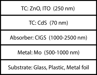
A thin-film solar cell is built around a semiconductor layer, where the light is absorbed and charge carriers (electron-hole pairs) are created, sandwiched by, on one side, the electron conducting layers, and on the other side, by hole conducting layers. At least one of these conducting layers must be transparent to the solar spectrum for light to reach the central “absorber” layer, see Figure 1. Each interface between two layers in a thin-film solar cell constitutes a heterojunction, which must be carefully tuned to optimize the overall performance of the solar cell. Current thin-film solar cells are built around either cadmium telluride (CdTe) or copper indium gallium selenide, CuIn1-xGaxSe2, (CIGS) as semiconductors for the absorber layer. Large scale deployment of these established technologies is potentially impacted by the toxicity (e.g., cadmium) or relative expense (e.g., indium) of some of the constitutent materials. Hence, the search for alternative absorber semiconductors focuses on earth abundant constituents that are nontoxic gs-scsearch_1 ; gs-scsearch_2 . For each new candidate material, new conducting layers, one of which has to be transparent, must be found and matched to each other by optimizing the heterojunction interface between each pair of layers.
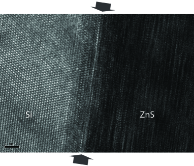
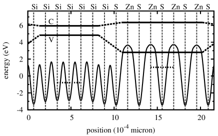
In current solar cell design an absorbed photon creates exactly one charge carrier pair with an energy equal to the bandgap of the absorber semiconductor material. The excess energy of the photon is lost as heat. Photons with energies in principle have enough energy to excite two charge carrier pairs. Multiple charge carrier generation from high energy photons is known as impact ionization (II) and is present in all semiconductors but not very efficient. Exploiting quantum effects to enhance II is an active area of research gs-II-lit_1 ; gs-II-lit_2 ; gs-II-lit_3 . It has been hypothesized that II can be efficient at the heterojunction interface of a low bandgap semiconductor host material (bandgap ) and a wide bandgap semiconductor with a bandgap at least twice as big as the bandgap of the host, i.e., . We refer to this hypothetical process as heterojunction assisted impact ionization (HAII) and a search for HAII is an ongoing research effort; see Figure 2 for a model heterojunction for HAII consisting of the wide bandgap direct semiconductor zinc sulfide ZnS and the low bandgap ’host’ semiconductor silicon Si.
A heterojunction is characterized by several parameters that determine its physical properties and affect the performance of a device. Most important are the valence band and conduction band discontinuities and (summarily referred to as band offsets, see Table 2), which can be obtained, in principle, experimentally. However, computations allow for a broader search for better photovoltaic devices.
Background on mathematical and computational models. The well known drift-diffusion model is the most widely used continuum mathematical model for semiconductor devices, and, in particular, for solar cells. We refer to Selber ; markowich86 ; markowich ; BankRoseF ; jerome-sdbook ; Jerome09 for extensive background and recent extensions. It can be derived from semi-classical transport theory based on the Boltzmann equation together with the Poisson equation and a number of assumptions, most importantly the introduction of a phenomelogical relaxation time and thermal equilibrium for the charge carriers. Even though these assumptions limit the validity of the drift-diffusion model to low energies and longer time scales, it generally provides an adequate description of the steady-state transport in solar cells, except in cases where its assumptions are explicitly violated, as is generally the case for all approaches to solar energy conversion that attempt to harvest high energy photons more efficiently (so called third generation photovoltaics Green06 ). More sophisticated models that includes high field and high energy effects as well as short time-scale phenomena, include hydrodynamic transport models that go beyond the Boltzmann transport equation (see for example Ref. 2 in FischettiLaux88 ), as well as particle based Monte Carlo models FischettiLaux88 ; Saraniti06 . See also Gamba06 for an example of coupling and comparison of hydrodynamic and Monte Carlo models. A computationally efficient approach would treat only the critical regions with a more sophisticated model, which is coupled to the standard drift-diffusion model to create a complete device simulation. Such an approach is the ultimate aim of our work on heterojunctions but is outside the scope of the present paper.
Despite the simplifying assumptions in the drift-diffusion system, it is quite complex, and presents challenges for analysis, numerical discretization, and nonlinear solver techniques. The difficulties include the nonlinear coupled nature of the system, the presence of boundary and interior layers, and the out-of-double precision scaling of data and unknowns, which render the model difficult to work with for computational scientists without prior experience.
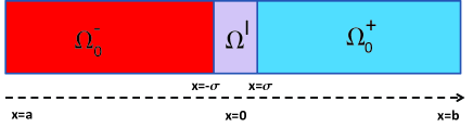
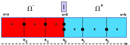
The presence of a heterojunction adds to that complexity. Consider a 1d semiconductor region made of two materials, with an interface region located near , as shown in Figure 3. Processes in where the two materials meet are characterized, e.g., by steep gradients and discontinuities of the primary variables, and cannot be resolved on the scale of drift-diffusion models.
One way to model heterojunctions is via an atomic scale model such as Density Functional Theory (DFT) in which however cannot simulate more than a few atomic layers MartinVanDeWalle1 . Alternatively, one can use an approximation of the interface region by a lower-dimensional interface Yang ; HorioYanai , as in Figure 3, along with a separate mathematical model approximating the physical phenomena across the interface. This is described, e.g., in HorioYanai ; Yang , and heterojunction models have been implemented, e.g., in community codes such as 1D semiconductor modeling programs AMPS ampsweb and SCAPS Berg2000 ; scapsweb . However, literature and documentary material for these as well as early modeling references such as HorioYanai ; Yang ; fonash1979 do not analyze the mathematical assumptions underlying the treatment of the interface, and many are quite subtle and unusual.
Ideally, one would find a way to tightly couple the continuum model away from the interface, i.e., in with some other model in the interface region , but this is not feasible yet. Instead, in this paper we take a step in the direction of a future coupled continuum–discrete model by decomposing functionally the continuum heterojunction model into subdomain parts on , and the interface part . In simulations we use realistic interface parameters computed by the DFT model on which is, however, entirely decoupled from the continuum model.
A substantial part of this paper is devoted to the careful modeling of the interface equations elucidating the challenges and unusual features as compared to the traditional transmission conditions in which the primary variables and their normal fluxes are continuous. We also reformulate the heterojunction model using domain decomposition method (DDM) quarteroniV which, to our knowledge, has not been applied to heterojunction models. (Throughout the paper we use DDM to denote concepts related to domain decomposition, in an effort to avoid confusion with the drift-diffusion equations). We present preliminary results of our DDM algorithm as applied to each step of the Gummel loop for homojunctions as well as to the potential equation for heterojunctions, and these results are promising.
DDM requires that we carefully examine the behavior of the primary variables and their fluxes across the interface. In fact, the former lack continuity, and the primary variables either have a step jump, or satisfy a nonlinear Robin-like condition. We find similarities of the heterojunction model to various fluid flow models that have recently attracted substantial attention in the mathematical and numerical community. Analysis in MoralesS10 ; MoralesS12 and modeling and simulations for flow across cracks and barriers in Roberts05 ; RobertsFrih have been pursued. See also recent numerical analysis work in GiraultRW05 ; GiraultR09 ; RiviereK10 ; RiviereA12 devoted to other flow interface problems. Still, the heterojunction problem appears even more complex than (some of) those listed above due to its coupled nature and nonlinear form of the interface conditions as well as to the complexities of the subdomain problems.
Clearly nontrivial mathematical and computational analyses following MoralesS10 ; MoralesS12 ; Roberts05 ; RobertsFrih as well as semiconductor-specific implementations are needed, but the formulation given here opens avenues towards applications of modern numerical analysis techniques beyond the finite differences that have been traditionally employed. In particular, the DDM solver given here can be easily extended to multiple interfaces or complex 2d geometries. In contrast, such extensions may be very difficult for monolithic solvers in which the interface equations are hard-coded. We plan to address 2d implementation in our future work.
The outline of the paper is as follows. We present an overview of the DFT model in Section 2. Detailed description of the subdomain and heterojunction interface models is given in Section 3. Here we also describe the domain decomposed formulation of the problem in which the interface problem is isolated in its own algebraic form amenable to an iterative solver, with particular care paid to the heterojunction formulations. In Section 4 we present computational results for the DFT, monolithic, and DDM solvers. In Section 5 we discuss and summarize the results. The Appendix in Section A contains some auxiliary calculations and data which support the developments in Sections 3 and 4.
2 Computational Model: DFT
Quantum mechanics of the electrons governs the properties of matter and hence the properties of a heterojunction. The direct solution of the quantum mechanical problem of an interacting electron system remains an intractable problem, but the reformulation in terms of the electron density of Hohenberg and Kohn and Kohn and Sham HK ; KS provides an indirect and, using appropriate approximations, feasible approach for many problems in condensed matter theory, materials science, and quantum chemistry. Density functional theory (DFT) has become the standard approach to calculate material properties from first principles. To set the stage for the calculation of heterojunction parameters and in particular band offset energies, we give a condensed overview of DFT loosely following and adopting the notation of PerdewKurthDFTprimerbook . For details we refer the reader to one of several monographs and reviews DFTprimerbook ; DFTadvancedbook .
2.1 Density Functional Theory
The large mass difference between electrons and nuclei allows us to treat the motion of the light electrons relative to a background of nuclei with fixed positions. DFT deals with the standard Hamiltonian of interacting electrons (ignoring spin for brevity)
| (1) |
which consists of the kinetic energy operator ,
the Coulomb interaction between the electrons,
and the interaction of the electrons with an external potential
The external potential contains the contributions from the atomic nuclei and possibly other terms. Here , where is the Planck constant, is the electron mass, is the charge of the electron, and is the quantum mechanical position operator for electron messiah99book .
The solutions of the stationary Schrödinger equation,
| (2) |
are the many-electron wavefunctions with energy . For the ground state with energy , the Schrödinger equation (2) is equivalent to a variational principle over all permissible electron wavefunctions,
| (3) |
The theorem by Hohenberg and KohnHK ; LL_1 ; LL_2 provides the existence of a density variational principle for the ground state,
| (4) |
where
| (5) |
is a universal functional defined for all electron densities . The ground state density (or densities if the ground state is degenerate) that minimizes (4), uniquely defines the external potential . Expressing ground state properties in terms of the electron density as in (4) defined over instead of a fully antisymmetric electron wavefunction defined over as in (3) is a huge reduction in complexity, but this simplification comes at a cost, since the functional is not known.
DFT requires suitable approximations for as well as efficient minimization schemes to determine the approximate ground state energy and electron density. The Kohn-Sham equations KS described next provide an iterative solution to the minimization problem and serve as the basis for approximate density functionals.
2.2 Kohn-Sham equations
A solution to (4) can be found for a system of non-interacting electrons governed by effective single electron Schrödinger equations,
| (6) |
where , denote eigenstate and energy of a single particle. Here we have introduced the electrostatic potential
consisting of the Hartree term of the Coulomb interaction between the electrons and the external potential. The electron density is given by and the Fermi energy is determined by the normalization condition for the density . Approximations for the functional from (5) enter through the exchange-correlation potential , which is the functional derivative of the exchange correlation energy with respect to the electron density:
| (7) |
The exchange correlation energy is the remainder of the functional , after the kinetic energy of the non-interacting electrons
and the Hartree energy
have been subtracted:
| (8) |
A self–consistent solution of the Kohn-Sham equations (6)-(8) can be found iteratively for a suitable choice of approximation of the exchange correlation energy .
A particularly simple and surprisingly effective approximation is the local density approximation (LDA)
| (9) |
where is the exchange correlation energy of the uniform electron gas electrongas_1 ; electrongas_2 .
Finally, the total ground state energy of the electron problem given by (1)-(5) can be calculated as
| (10) |
The Kohn-Sham equations are a system of coupled single particle wave equations, but their computational cost increases rapidly when non-local approximations for the exchange-correlation potential are used. The Kohn-Sham equations not only provide an efficient numerical tool to solve the density variation principle (4), but they are equivalent to the well known bandstructure equations of the independent electron approximation. It is worthwhile to note however that DFT gives no additional justification for the use of the independent electron approximation. The single particle eigenstates with single particle energies appear merely as reference system to solve the complicated interacting problem in an approximate but highly useful way. They are used extensively because they provide excellent results for many properties for an exceedingly large number of systems in condensed matter physics, materials science, and quantum chemistry.
2.3 Semiconductors properties
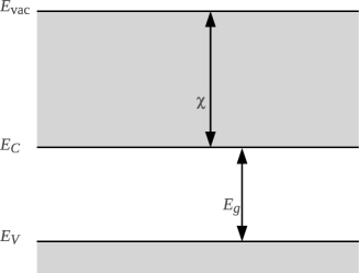
For an intrinsic semiconductor (undoped, zero temperature) the valence band energy is the energy of the occupied single electron state with the highest energy, and the conduction band energy is the energy of the unoccupied single-electron state with the lowest energy. The bandgap is the minimum energy required to remove one electron from the occupied single particle states, the valence band, and add it to the unoccupied states, the conduction band, and is given by the difference (see Figure 4). The electron affinity denotes the energy required to add one electron to a semiconductor and is given by the difference of the electron vacuum energy and the conduction band energy .
As is customary in semiconductor device modeling, we define the potential . In terms of the potential the semiconductor quantities that enter the continuum model are defined as
| (11) |
The bandgap of a semiconductor is a ground state property and can be expressed in terms of ground state energies as in (4). For a semiconductor with electrons it is denoted by so that
In practice however, the bandgap is calculated in terms of the single electron states and energies that are the self-consistent solutions of the Kohn-Sham equations (6), and
Local approximations of the exchange-correlation energy (8), like the LDA (9), typically result in bandgaps that are too small eg2small . This negative result is well understood, and improved approximations allow the accurate prediction of bandgaps from first principles Kresse .
In preparation for the calculation of band offsets from periodic supercells described in the next section, we define and calculate a local reference energy , where is the electrostatic potential defined in equation (2.2). The electrostatic potential is spatially averaged over the entire unitcell of the semiconductor to determine the average electrostatic potential, . Our choice of reference energy is not unique but a convenient one for electronic structure methods based on planewave basis sets.
2.4 Band offset calculation
We formulate the heterojunction problem in terms of a supercell surrounding a section of the interface MartinVanDeWalle1 ; MartinVanDeWalle2 . Periodic boundary conditions are used in all spatial dimensions. The supercell dimensions in the plane of the interface are determined by the periodicity of both semiconductor lattices. The length of the supercell must be sufficiently large so that away from the interface both semiconductors have essentially bulk-like properties. The use of periodic boundary conditions allows the application of the same computational tools to the interface problem that have been developed for bulk materials. On the other hand, some complications may result from the use of periodic boundary conditions, e.g., one ends up with two heterojunctions which are symmetric only in simple cases such as for the Si/ZnS heterojunction shown in Figure 5. Periodic boundary conditions may be used, even in the case of two different (asymmetric) interfaces, provided the supercell is long enough to distinguish the rapid band behavior at a single interface from slow, artificial changes that may occur due to the boundary conditions. (The slopes of the bands present in continuum model solutions are not modeled in this calculation, and are considered infinitesimal on the scale of the supercell.) The interface atomic structure of the heterojunction is generally not known and can be determined, in principle, within the constraint of the boundary conditions of the supercell by minimizing the energy of the supercell as a function of the atomic positions.
To determine the valence band energy separately for both semiconductors in the supercell, we calculate the local reference energy defined in the previous section, but now the average over the electrostatic potential energy is taken for each semiconductor separately over a finite region in the supercell, where each semiconductor has essentially bulk-like properties (see Figure 5). The accuracy of the averaging procedure can be systematically controlled by increasing the size of the supercell used for the interface calculation. We can relate the energy difference for both semiconductors in the supercell with the corresponding energy difference in the separate bulk calculations. For the heterojunction shown in Figure 5 we obtain, for silicon,
Similar equations follow for the other semiconductor (ZnS in our example). The valence and conduction band energy offsets are the differences and .
3 Computational Model: continuum
Here we present the continuum model for a semiconductor device with an interface. Our presentation of the drift-diffusion models is based on Selber ; markowich86 ; markowich ; MarkRS , with analysis as presented in markowich ; jerome-sdbook while the interface physics and model have been described in Sze ; HorioYanai ; Yang .
We use the geometrical representation presented in Figure 3. Recall that, while the approximation is convenient for a continuum model, it is a simplification of the real physical situation, in which the interface region is composed of a few atomic layers.
First we describe the drift-diffusion equations, a coupled system of nonlinear PDEs, with coefficients which depend on the material from which are made. Next we describe the interface model, its numerical approximation, and the domain decomposition formulation. The various coefficients are given in Tables 1, 2 and depend on the material and the type of interface.
| symbol | parameter | |
|---|---|---|
| net doping profile | ||
| trap-related electron lifetime | ||
| trap-related hole lifetime | ||
| direct recombination coefficient | ||
| dielectric constant | ||
| electron affinity | ||
| intrinsic carrier concentration | ||
| bandgap | ||
| density of states, conduction band | ||
| density of states, valence band | ||
| electron diffusivity | ||
| hole diffusivity | ||
| effective Richardson’s constant for electrons | ||
| effective Richardson’s constant for holes |
| symbol | parameter | |
|---|---|---|
| jump of potential | ||
| jump of conduction band energy | ||
| jump of valence band energy |
Notation: We adopt the following notation for the continuum model. The dependence on some independent or dependent variables is omitted if it is clear from the context. In particular, we use for the recombination terms which depend on the variables , , as well as on several position dependent parameters. The same concerns various material parameters, whose dependence on the position , and in particular on the type of material, i.e., whether , or , is dropped. When relevant, we denote material dependent constants using superscripts . Also, we denote by the characteristic function of , i.e., the function equal to one in and to zero elsewhere, and is defined analogously. These help, e.g., to write a piecewise constant material dependent coefficient, e.g., .
We use notation to denote a unit vector normal to a boundary or interface pointing outward to the given domain.
We distinguish the value of a physical quantity evaluated on the left side of . With the geometry as defined above we have
| (12) |
We also use the notation
Similar notation, when , is common in computational mathematics and in particular in numerical analysis of Discontinuous Galerkin (DG) Finite Element methods riviere-book , where the symbols
are used at computational nodes (here at ). The context in which we use , is different from the DG-specific use of , respectively, since .
To make this distinction clear, in the model derivations we use across a homojunction interface , and across a heterojunction approximating some . The case of a homojunction and is when the materials in are the same, but the doping characteristics change drastically across . The case of a heterojunction and is when the materials are different, and there are additional physical phenomena that need to be accounted for in , i.e., across .
Throughout the paper we use, to the extent possible, nondimensional quantities, while keeping material-dependence evident through notation. Our use of nondimensional quantities is consistent with typical scaling applied in semiconductor modeling such as described in Selber . When needed for clarity, we emphasize this by referring to the “scaled units”.
Finally, we use notation of functional spaces as traditionally adopted, e.g., in ShowDover ; BrezziFortin ; quarteroniV . In particular, is a space of functions of up to continuous derivatives on . For weak formulations we use Sobolev spaces instead of , where we recall . Also, is the space of essentially bounded functions.
3.1 Bulk equations in a homogeneous semiconductor
We assume isothermal and steady-state regimes. While transient behavior has decayed, the time-independent transport of electrons and holes is described by the spatially-dependent electron and hole currents. These currents are steady-state responses to certain boundary conditions (applied voltages), bulk carrier generation due to illumination, and other carrier sources and sinks such as electron-hole recombination.
For convenience we are presenting the continuum model in terms of dimensionless quantities. Each quantity is scaled by a dimensioned quantity and may be scaled by a length quantity. The scaling is discussed further in Appendix 1.2.
The drift-diffusion model in a single-material semiconductor domain is
| (13) | |||||
| (14) | |||||
| (15) |
Here are, respectively, the potential and the charge densities of holes and electrons, and is the given net doping profile including the donor and acceptor doping . The recombination term is defined below.
The current density where the drift part is due to the electric displacement field and the diffusive part . Thus we have
| (16) |
Similarly, the flow of holes is described by
| (17) |
For convenience of numerical computations the currents can be defined with the use of the quasi Fermi potentials as
| (18) | |||||
| (19) |
where and are related via Maxwell-Boltzmann statistics
| (20) | |||||
| (21) |
To see why (18) and (16) are equivalent, we differentiate (20) to see . Of course, this change of variable is only possible if are differentiable, and, in particular, is not true at heterojunctions across .
The recombination term is given as in [Sze , Sec 1.5.4] by
| (22) |
Here is a position-dependent carrier generation source term from the light sources. The terms and are given traditionally as Shockley-Reed-Hall recombination terms
| (23) |
| (24) |
The parameters are material constants given in Table 1, and .
When analyzing well-posedness, or numerically solving the model (13)–(15), one has to make a decision on the choice of primary variables. While are most physically natural, two other sets of variables , as well as so-called Slotboom variables can be used. The Slotboom variables are defined as
| (25) |
where is a scaling parameter that depends on the material as well as the doping profile . Similarly to (20)–(21), this change of variables only works if are smooth, thus, not across .
3.2 External boundary conditions
To complete the model (13)-(15) as a boundary value problem, we need external boundary conditions on . What follows is a summary of, e.g., [markowich86 , Sec. 2.3].
We use Dirichlet conditions for (13),
| (29) |
To determine physically meaningful values of one finds first the neutral-charge thermal equilibrium values of , i.e., solving, e.g, at , the algebraic problem solved for
This corresponds to setting everywhere on , and dropping the derivatives from (13). At we solve a similar equation for . The neutral-charge thermal equilbrium conditions are appropriate for sufficiently long single material domains with “ideal” contacts with external metal regions.
With we set
where and are physically controllable external (scaled) voltages; see Section 4.1 for their use.
The boundary conditions for (14)-(15) are specified using the individual carrier currents via contact-specific effective recombination velocities , , , and . In scaled units these Robin conditions read
| (30) | |||||
| (31) | |||||
| (32) | |||||
| (33) |
Here are the carrier densities corresponding to the thermal equilibrium values via (20)-(21).
3.3 Well-posedness in a single material
We recall now after markowich the basic information concerning well-posedness of the system. The Gummel iteration introduced here is relevant for the numerical solver as well as interface decomposition procedure.
Let , with the norm inherited from . To analyze existence and uniqueness of solutions to (13)–(15), under boundary conditions (29)-(33), one uses Slotboom variables .
The most important technique is to use the Gummel Map , a decoupling procedure, subsequently analyzed as a fixed point problem. Formally, given , one solves the potential equation (13) rewritten with (25)
| (34) |
for . Then we solve the n-continuity equation
| (35) |
for , and the p-continuity equation
| (36) |
for . The equations (34)–(36) are supplemented with appropriate boundary conditions.
The system (34)–(36) is the iteration-lagged system (13)–(15) under a change of variable formula (25). The existence of a solution to the system (13)–(15) with (25) follows from first i) establishing existence of solutions for each of the semilinear elliptic equation (34) and the two linear elliptic equations (35) and (36). Next ii) one establishes the existence of a fixed point of the Gummel Map. Step i) can be accomplished with standard techniques from elliptic theory and functional analysis, while ii) the existence of a fixed point of the Gummel Map is established from the application of the Schauder Fixed Point Theorem, assuming that the data is small enough. A thorough analysis of the preceeding, as well as of regularity results, is given in [markowich , Sec. 3.2,3.3].
As concerns uniqueness, one can show that under small enough external applied voltages, the solutions are unique and depend continuously on the data. However, under certain physical conditions, multiple solutions to the stationary drift-diffusion model are known to exist. e.g., for large data. A detailed exposition on uniqueness and continuous dependence on data can be found in [markowich , Sec. 3.4].
We note that there is no well-posedness theory available for the heterojunction interface problem described next.
3.4 Interface equations
The first issue in an interface model is to identify which quantities are conserved and which variables are continuous across that interface. Some of these considerations are directly related to parameter dependent material constants, which vary across .
At a homojunction, all material parameters such as are constant, and the primary variables , as well as their normal fluxes , , are continuous. Thus the equations (13)–(15) hold in the classical sense. However, takes a jump .
At a heterojunction, one has to recognize two facts. First, the material properties are not continuous across the interface. Second, there are physical phenomena happening in which cannot be described by the drift-diffusion model. Thus, in the approximate geometrical decomposition , each of (13)–(15) must be replaced by a separate model statement on . In particular, even though across the potential as well as charge densities are continuous, these variables are not continuous across .
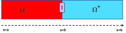
The discontinuities pose issues for the mathematical model. If primary variables are not continuous at a point , then their derivatives and normal fluxes across cannot be rigorously defined. At the same time, we recognize that a jump of a quantity across the interface is an artifact of geometrical approximation . Thus one can argue on the basis of physical modeling and observation what should be the interface equations satisfied on . These conditions on are to be understood as internal boundary conditions that decompose the original boundary value problem on into two independent boundary value problems on , , joined by a separate interface model posed at .
Below we make the interface model on precise. We first recall the classical transmission conditions for a generic elliptic equation with piecewise constant coefficients. This part is appropriate for a homojunction and helps to set the stage for the heterojunction model discussed next. Across a heterojunction we consider the quantities as well as the derived quantities , and the normal fluxes , etc. Next we discuss the algebraic form of the transmission problem to guide our numerical domain decomposition formulation for heterojunctions discussed in the sequel.
To our knowledge, its mathematical and approximation properties have not been analyzed and many are quite subtle and unusual.
Transmission conditions for an elliptic equation at a homojunction: Assume that a variable with a flux satisfy a second order Dirichlet boundary value problem in
| (37) |
where are given data. (Here we use notation of the potential equation (13) assuming that is given.)
In order for (37) to have a classical solution , the data must be continuous on and in particular at .
Since in many practical applications when interfaces are present this does not hold with , , one considers weak solutions to (37) in which only are assumed to be continuous across . The weak (generalized) solutions to (37) are sought in the Sobolev space instead of in , see, e.g., ShowDover for details on weak solutions of elliptic problems. In particular, if is a piecewise constant coefficient, and is a piecewise constant source term, as long as , then the problem (37) is well-posed and has a weak solution with . The well-posedness in appropriate Sobolev spaces is a necessary condition for a proper formulation of finite element discretizations for (37), while (at least) regularity is, in general, needed for convergence of finite difference formulations.
When solving (37) numerically, one frequently finds it convenient to use domain decomposition (DDM) quarteroniV . Thereby one writes the differential equation (37) that must be satisfied in each . Additionally, we write the interface transmission conditions that need to hold at . These are
| (38) | |||||
| (39) | |||||
| (40) | |||||
| (41) |
Further information on analysis of transmission problems with piecewise constant coefficients can be found, e.g., in [ShowDover , III.4.4].
The transmission conditions (40)-(41) describe the qualitative nature of , and are sufficient to close the system. The discretized version of (38)–(41) is uniquely solvable and gives the same solution as the discrete version of (37), as long as appropriate treatment of (41) is used.
In view of the heterojunction interface model to be developed shortly, we remark further on the equations satisfied at , since in numerical point-centered formulation some equation must be posed for a node located at . We develop these equations for simplicity in 1d, by a calculus argument.
At a first glance it appears that the information that (37) holds at is lost. To see that (37) actually does hold at , assume that (38) and (39) hold pointwise, i.e., that is continuous on each of . Then integrate (39) and (38) over and , respectively, with chosen so that these intervals are inside . We obtain
| (42) | |||
| (43) |
We add the two equations, divide them by , and pass to the limit with . This gives .
| (44) |
Note that (44) is derived from (38)-(39) entirely independently of (40) and (41).
If is continuous and (40)-(41) hold, we get
| (45) |
thus the fact that (37) holds at is recovered. Conversely, the continuity of across itself, without (40), (41), does not guarantee that (45) makes sense, as the example of demonstrates.
We elaborate on the algebraic form of (38)–(41) used in numerical domain decomposition in Section 3.6.
We proceed next to define proper interface equations for the potential and the continuity equations.
Potential equation at heterojunction: Assume that (13) holds in and , with appropriate boundary conditions at . To close the system, we need to make precise the conditions at , i.e., on and that of . Recall that the data in this equation are discontinuous at a heterojunction, and that may not be continuous even at a homojunction.
It is known that is continuous across . However, since must follow the energy bands, its restriction to and is discontinuous, and we have
| (46) |
where is given, see Table 2.
The case corresponds to one of the three possibilities. First, i) either that is, we have no interface region and represents a homojunction. Or, ii) the potential is constant across , which would mean however that the current vanishes, i.e., that is an insulating interface. The third possibility iii) is that the potential varies in such a way across that , and this does not happen at a heterojunction.
As concerns the field , it has been customary to assume that
| (47) |
It is important to comment that (47) describes the shape (slope) of at and is not a statement on derivatives of a function . Since by (46) is discontinuous across , it is not differentiable there. However, since the width of is very small, it is believed that there is no additional net “Dirac-delta” charge to make .
Now (46) and (47) are sufficient to close the system, which has a structure similar to that of DDM-like formulations, except with a nonhomogeneous jump. We illustrate this further in Section 3.6.
Finally, it is not necessary to specify whether (13) holds at , since any such statement should be a consequence of the interface equations (46)-(47) in a manner similar to how (44) was derived. However, we derive its counterpart for modeling interest. Consider integrating (13), i.e., , over and , for some . Assuming is continuous on each of these intervals, we obtain, similarly as in (42), (43),
Adding these equations, dividing by and letting we obtain,
| (48) |
This equation, when , has a structure of (44) applied to (13). Appropriately, if , and is continuous, we obtain that (13) is satisfied pointwise at .
We stress that (48) is a consequence of (13) being satisfied away from , and is independent of (46)-(47). Whether or not (48) is used at , depends on whether the discrete equations are posed at . Equation (48) is not significant if only weak solutions are sought.
Continuity equation at heterojunction: The data in (16), (17) are discontinuous across , and is continuous only if are. Additionally, we have (47). We can still write similarly to (48) that
| (49) |
which follows simply from (16) and is similar to (48). However, we need to specify whether , are continuous across , and if not, we need a model binding . (Similar questions concern .)
To do so, we use a model used in physical engineering literature HorioYanai ; Yang , which does not have the same “DDM-like” formulation as that given for potential equation by (46) and (47). In contrast, we have an explicit interface model for which can be interpreted as an internal boundary condition, and is based on the notion of the thermionic current proportional to the jump of , with a proportionality constant dependent on the electron masses in each domain.
Early models of heterojunctions assumed is continuous across and did not use . However, just like , the variables and are continuous across , but neither is continuous across the “idealized” interface . From (20) we see that discontinuity of across parallels that of , since . Thus we have variables that need to be related to , and this is done as in HorioYanai ; Yang
| (50) |
The coefficients in (50) are, up to the scaling, mean electron thermal velocities, and they are calculated depending on the temperature and on the sign of .
For example, let so that the conduction band jumps up a positive amount. Then
| (51) |
Here is the effective Richardson’s constant (effective electron mass), and is the temperature.
If , the conduction band jumps down, and we have
| (52) |
The -equations are similar except with the valence band gap in place of . Similar to (50), we have
| (55) |
If , then the valence band jumps up a positive amount and we have
| (56) |
If , the valence band jumps down and we have
| (57) |
It is important to note that the model defined above is appropriate at a heterojunction only. At a homojunction with we have , , and we expect . Since then , one could then infer (incorrectly) from (50) that ; however, the current need not vanish across . Rather, at a homojunction we have .
In summary, the interface conditions for (16) are
| (58) |
| (59) |
A similar condition is formulated for the transport of holes.
We note that (59) is similar to (47), but (58) is unusual, and is an internal Robin-type condition. It is similar to external boundary conditions (30)–(33) that are used for continuity equation. Such external boundary conditions for Schottky contacts have been defined, e.g., in [markowich86 , Sec. 5.4].
Mathematically, (58)-(59) resemble closely the conditions that arise for modeling fluid flow in fractures MoralesS10 ; MoralesS12 ; Roberts05 . These are best analyzed using a different functional setting than that in . We comment on these further in Section 3.5.
The algebraic structure of this interface problem is discussed in Section 3.6.
3.5 Numerical approximation
Here we discuss the discrete formulation for the subdomain models, followed by discretization of the heterojunction interface model.
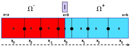
Grid. We first discuss the underlying discretization. The equations (13)–(15) can be discretized using finite difference (FD) or finite element (FE) formulations, see markowich . In the 1d case, the FD and FE formulations are based on a point-centered gridding of the domain, see Figure 6. Typically, one seeks nodal values , approximating the primary unknowns such as , at grid points distributed in . For simplicity, we consider a uniform grid with parameter , and , as in Figure 6. The flux values of are approximated at .
Most of FD and (Galerkin) FE methods are based on point-centered discretizations and such are those in markowich , even though some semiconductor modeling work chen-cockburn1d ; chen-cockburn2d has been carried out with mixed FE methods. We refer to BrezziFortin for fundamental reference to mixed FE methods, and recall that mixed FE on rectangular grids and with lowest order spaces, and appropriate quadrature, give cell-centered approximations RW such as that shown in Figure 6, bottom. Mixed spaces were used, e.g., in the modeling and analysis efforts in Roberts05 ; MoralesS12 . They were also used extensively in numerical and domain decomposition approaches for fluid flow where continuity of fluxes is essential, see, e.g., GW ; ACWY ; PIMA00 ; YIMA00 . We intend to consider mixed FE and cell-centered grids in future work, since these remove the need for doubling interface unknowns, and may make interface equations more natural.
In what follows we use point-centered grids.
FD formulation of the system (13)-(15). We recall uniform point-centered grid discretization of (13) which at node , for constant on reads
| (60) |
with . In particular, if we assume Dirichlet boundary conditions for the potential, (60) has the form
| (61) |
where , is the tridiagonal matrix based on the discrete 1d Laplacian leveque-fdbook . has numbers on its diagonal, and below as well as above its diagonal. Also, is the vector of charges, depending pointwise on . Boundary conditions (29) are included in the right side of (61) in a standard away leveque-fdbook .
The challenges in the discretization of (14)-(15) include the proper handling of boundary and internal layers and of steep gradients. One uses then a special choice of primary unknowns such as the approximations to , instead of approximations to . The nonlinear expressions such as those from (28) with (20) must use appropriate weighting.
Consider, e.g., the electron equation (14), whose discretization, with (28), reads
| (62) |
where the coefficient depends on , and typically is defined with the use of exponential weighting, i.e., Bernoulli’s function, as elegantly described in [BankRoseF , eq.55], [markowich86 , Sec. 5.1], Selber . The exponential weighting is known to help with internal boundary layers as well as to stabilize the nonlinear solver.
Now (62) can be written in a way similar to (61)
| (63) |
and it comprises external boundary conditions (30), (32). Here , and the dependence of and on was supressed since it is iteration lagged, as explained below. A similar equation is defined for the transport of holes.
In summary, in what follows we refer to the unknowns as , and to the equations to be solved as
| (64) |
written componentwise as
| (65) | |||
| (66) | |||
| (67) |
These correspond to the discretizations of (13), (14), (15), respectively, with (20)–(21), and appropriate boundary conditions. In particular, (65) is the same as (61) written in residual form . Similarly, (66) is (63) in residual form.
The system (64) is solved typically with a variant of the Newton method. The very well known Gummel iteration is similar to that recalled in Section 3.3 solving first (65) for , given previous iteration guess, or initial guess, for . Next one solves (66) for , and (67) for using the newly available guesses for the , and , respectively. The Gummel iteration continues until tolerance criteria are satisfied. With a well chosen set of unknowns, each of the component equations being solved is self-adjoint in its primary variable. With additional iteration lagging and appropriate choice of unknowns, each equation is linear or semi-linear in its primary unknown.
However, as is well known, Newton’s method is not globally convergent and may fail if good initial guesses are not available. In practice, the cases with large gradients and “difficult data” are handled with extra caution, applying, e.g., method of continuity (homotopy) whereby one starts with small data and gradually increases it to the desired value. See Selber for practical information.
Gummel iteration itself may fail at times. One situation in which this may happen is when a spike in or forms, and intermediate solutions cause the effective potential quantities to intersect the spike, creating very large carrier concentrations. Recovery from this situation can depend on the choice of variables used in the Newton method solvers. We have seen Slotboom variables outperform variables in this situation. Using the and variables has caused problems even in a single bulk material when doping is significant. Various situation-dependent tricks have been used over the years in the community solvers ampsweb to control the behavior of nonlinear iterations but it seems that a general remedy has not yet been found.
Heterojunction. To simulate the behavior of for a heterojunction problem, one has to implement, in addition to the discrete equations in (65)–(67) to be solved in each of , the discretized interface equations described in Section 3.4.
In particular, since are discontinuous at , this requires doubling the unknowns at the grid point . From now on this is denoted by considering , with and . Also, we collect all the unknowns corresponding to in and those for in . The notation is inherited by each component of .
Now each component of (64) can be written as two subdomain problems coupled to an interface problem. For example, consider (65) with the two subdomain problems written as
| (68) |
where the dependence of on reflects that provides the boundary values for , etc. Now (68) must be complemented by discretization of the interface equations so that gets connected to . In fact, only the interface unknowns , and their nearest neighbors are involved in the interface model due to the locality of the three-point FD stencil in (60). We denote the discrete interface problem by
| (69) |
and give its details in Section 3.6.
A similar decomposition follows for the discrete continuity equations (66)-(67), at each step of the Gummel iteration.
Once the discrete equations are known, one must design the implementation of the doubling of the unknowns as well as the connection of the subdomain (68) and the interface equations (69) in the solver.
In various community or commercial codes this is apparently achieved in 1d by a monolithic approach, i.e., the interface equations are hard-coded internally. In particular, in Gummel iteration one solves (68) and (69) for simultaneously. This is followed by solving for all the subdomain and interface components of (66) for , and the loop completes with solving (67) for .
While it is perhaps easy to see how to implement these simultaneous solves in 1d, it may be challenging or impossible to use this approach for complicated heterojunction geometries in 2d.
Therefore, in this paper we isolate the interface equations from the subdomain equations with a two-fold goal. First, we discuss an alternative approach to simultaneous solution, based on domain decomposition method. We identify the structure of the equations as well as pinpoint the difficulties, and this provides the basis for future analyses and extensions. Second, isolating the interface from the subdomains can help to handle more general geometries, and/or implement higher order methods, adaptive gridding and more. In particular, while for the current 1d formulation it is easy to place the computational nodes on the interface , a general approach from the class of immersed interface methods (IIM) GongLiLi can be helpful to develop a solution technique for a problem in 2d with complicated geometry. While IIM were originally developed for problems with homogeneous jumps, there is recent work devoted to complicated interface problems with nonhomogenuos jumps KwakCMAME ; HeLinLin .
3.6 Domain decomposition
Domain decomposition quarteroniV was originally designed to accelerate or simply enable the solution of problems which were too large to fit in a single computational core. It has since been shown to be very effective for problems with interfaces which separate either different materials or different physical models such as in fluid-structure interactions or Darcy-Stokes fluid flow problems quarteroniV . Its mortar extensions BerMadPat ; ACWY ; PIMA00 ; PWY02 ; YIMA00 ; LPW02 can be used to glue together different numerical discretizations on grids that need not match on the interface.
Domain decomposition methods (DDM) generally are iterative methods that find the values of interface unknowns so that a proper match between the subdomains is achieved. We refer to [quarteroniV , Chap 1-2] for general background which covers DDM for the transmission problem laid out in Section 3.4.
DDMs are tied to optimal solvers and preconditioners. In this context, see Lin09 and its recent extensions which focus on multilevel-preconditioning of non-stationary drift-diffusion systems, without heterojunction. The gist of the work in Lin09 is to consider a fully coupled system solved with the Newton-Krylov framework with multilevel preconditioning, and DDM applied here is a purely computational technique unrelated to the presence of physical interfaces. It will be interesting to consider in the future how to design optimal preconditioners following Lin09 for the heterojunction problem considered in this paper, and we hope it can complement the domain decomposition approach of this paper which follows naturally the material discontinuities.
In this paper we consider a non-overlapping DDM for solving an interface problem (69) coupled with subdomain solvers (68). The algorithm we outline has a double set of interface unknowns instead of a single as in the traditional set-up. It handles nonhomogeneous jumps of the primary unknowns and can also handle nonhomogeneous jumps of the flux(es). We have applied it successfully to the solution of the potential equation at both homo- and heterojunctions, and to the continuity equation at a homojunction. The interface iteration for continuity equations at a heterojunction is currently in progress.
3.6.1 DDM for the potential equation
We discuss first DDM for the algebraic problem that corresponds to the discretized form of (61) for the potential equation at a homojunction, i.e., with a single interface unknown . Ordering the unknowns so that we have the following system
| (79) |
which has the classical form (up to notation) from [quarteroniV , Sec 2.3]. Here is the part of matrix corresponding to the interior nodes of , and represents the coupling between the nodes in and those at . Also, , while is just a number, i.e., a matrix. etc.
The DDM is an iterative method for solving the system in the Schur-complement form
| (80) |
where we obtain by block elimination, e.g.,
| (81) |
from (79) that , and . The problem (80) has a simple structure thanks to linearity of (79). See Section 1.4 for the calculations of which includes (80) as a special case.
It is well known that one does not form explicitly. Rather, we use its structure and properties in an iterative solver for (80), which subsequently only requires subdomain solvers. In particular, an iterative solver delivers quesses , and requires that we compute a matrix-vector product for a given guess . This in turn requires that we evaluate, e.g., , where is not needed explicitly. Rather, a linear system with is solved, and this corresponds to solving a problem on the subdomain using the boundary conditions on provided by . A new guess is computed depending on the residual of (80); the details depend on the choice of interface solver, see Section 4.3.
Equivalence to the transmission problem and doubling interface unknowns for homojunction. One can easily show that (79) is equivalent to discretizing (37) in the transmission form (38)-(41). First, we recognize that the first two block rows of (79) are the discrete counterparts of (38)-(39). Each includes the coupling to the interface unknown used as a boundary condition. We can also formally double the unknowns and replace by on the interface. Then we enforce (40) explicitly by setting them equal to each other.
With doubling of the unknowns on the interface the system (79) becomes
| (94) |
The last row of (94) expresses (40), thus we can eliminate one of the two values , and the system reduces to (79). Note that we have intentionally mixed the symbols for matrices with those for numbers in the last row.
The second row from below, (and equivalently, the last row in (79)), can be shown to follow from the FD discretization of (41) using a second order accurate formula on each side of , followed by a discrete equation (60) to be satisfied at involving ghost nodes. See Section 1.3 for details.
Accounting for the jump of potential on the interface for heterojunction. Now we extend (94) and define the algebraic problem arising in the potential part of the Gummel iteration (65) with a heterojunction. We have a given and we need to solve an appropriate counterpart of (60) for .
With the notation as above, we place a computational node at , and seek approximations to so that discretized versions of (46) and (47) are satisfied. In addition, we modify the matrices in (94) to account for the values of . We also modify the right hand side in the last row of (94) to account for the nonhomogeneous jump in across , and we let replace per (48).
We obtain
| (107) |
We refer to Section 1.3 for details. Now if , then (107) reduces to (94) and further to (79), if also .
One can write an explicit calculation to set up an interface problem similar to (80)
| (108) |
The matrix now accounts for different values of on the interface and includes .
3.6.2 DDM for continuity equations
Next we proceed to define the algebraic problem corresponding to (66), with particular attention paid to interface equations at homo- and heterojunctions. A formulation for (67) can be written similarly.
Homojunction. First we see that we can rewrite (62) in a DDM form for the homojunction similarly to (94) written for (60) with the matrix calculated using the coefficients instead of the constant . The unknowns are , and the right hand side vector is now , where the last entry follows from the continuity of at a homojunction, reflected in the discrete problem by .
The structure of the appropriate algebraic problem to be solved for is thus entirely analogous to (94). The major difference with respect to (94) is that the components of the vector depend nonlinearly on the unknowns . The same concerns the coefficients , thus .
The nonlinearity does not change the structure of the analogue of (79) for homojunction, but a simple reformulation with a Schur-complement as in (80) is no more possible, since block elimination is not available and, e.g.,
| (111) |
replaces (81). However, at least theoretically, we can derive the nonlinear counterpart of (80) from (111)
| (112) |
After linearization (or in a Newton step, or via Gummel iteration-lagging), one can identify the domain decomposed blocks of the nonlinear system analogous to those in (80).
Heterojunction. We now outline the DDM version of the heterojunction system in analogy to (107).
We have (59) similarly to (47), therefore the third row of our system will look alike (107). We write it properly as (see also (147) in Appendix)
| (113) |
and recall that the coefficients depend nonlinearly on the values of and . In the block form we have therefore
| (114) |
where we identify , and , and other definitions can be completed similarly to those done for (79), (94) and (107).
Next, instead of a Dirichlet-like condition (46) which has a simple discretization in the last row of (107), we have the Robin-like condition (58). We discuss its discretization and structure next.
In order to discretize (58) to second order accuracy, we should use the ghost variables as in the derivation leading to (94), as is done carefully in Section A for the potential equation. An alternative is to use a first order, one sided approximation to ; see Section 1.3 and (143) for details on one-sided derivatives at the interface.
However, by (18) we have to deal with nonlinear dependence of on the variables involved. Thus, even though the first order approximation is less accurate, it appears also to be the most straightforward. We describe it here and leave the more accurate formulation for future work.
We approximate and set as the discrete counterpart of (58)
and a simple reformulation gives us finally
| (115) |
where the left hand side of (115) depends nonlinearly on , and on via .
We are then ready to state the analogue of (107) for the electron continuity (66) equation
| (126) | |||||
where the definitions follow directly from (115).
One could formally eliminate the (block) unknowns in (126) and set-up the nonlinear Schur-complement formulation extending further the nonlinear homojunction case (112) and the linear heterojunction case (108) to
| (127) |
Note that (127) involves untangling of the nonlinear relationship between and from the last row in (126), as well as other nonlinear relationships from other rows similarly to those in (111). We won’t pursue the explicit form of or of from (127) since these are not needed by the actual iterative solver for (127). While we have successfully solved (112) with an algorithm similar to that for (80), and have some preliminary results on solving (127), details will be given elsewhere.
4 Results and examples
In this section we present computational simulations of processes at heterojunctions, and in particular those supporting the search for more efficient solar cells.
In Section 4.1 we show DFT and continuum model results for Si/ZnS which emphasize the two scales present in the problem. In Section 4.2 we present results of a continuum model for a common solar cell CIGS/CdS heterojunction, and demonstrate the photocurrent. In Section 4.3 we focus on the DDM solver and study its performance, first for a Si homojunction, and next for heterojunctions. Here we consider three heterojunctions: silicon-galium arsenide (Si/GaAs), silicon-zinc sulfide (Si/ZnS), and copper indium galium selenide-cadmium sulfide (CIGS/CdS). (As concerns CIGS, we use the alloy semiconductor CuIn1-xGaxSe2, where is the ratio of the number of atoms of Ga to that of Ga plus In. Typically, for thin film solar absorbers.).
Since the DDM for the continuity part of the heterojunction model (66)-(67) is still under development, we use the monolithic solver for the continuum model in Sections 4.1-4.2.
We use m for Si/ZnS in Section 4.1, also m in Section 4.2, and m in all DDM examples in Section 4.3. The interface in all sections is always at . All calculations are assumed to be done at “room temperature” or K, and material constants are listed in Section 1.1.
In Sections 4.1 and 4.2 we use the conventional band diagrams depicting the energy levels for the electron , and defined in (11). Also, at thermal equilibrium, we have where the Fermi level is defined only in thermal equilibrium, and is always constant in a single body or device throughout which electrons may move to reach an equilibrium distribution. Without loss of generality we set , which is consistent with what was done in Section 3.2.
4.1 Results of DFT and continuum models for Si/ZnS interface
Here we first discuss the DFT model calculation of for Si/ZnS. Next we compare the results of the continuum model using this value and an available experimental value. The results are illustrated together in Figure 7, where the post-processed DFT results over are shown along with atomic structure of , followed by results of a continuum model where, as we explained in Section 1, .
Our study of both DFT and continuum models of the Si/ZnS interface is motivated by fundamental interest in polar interfaces harrison78pol ; nakagawa06why as well as by the hypothesis of HAII, as discussed in Section 1. Our DFT model examines atomically distinguishable Si/ZnS interfaces having the (111) normal orientation of energetically stable interface defects. A quantum mechanical and electrostatic analysis of single atom defect variations for other crystal orientations (111), (100), and (011) in Si/ZnS will be presented elsewhere foster13unp .
The DFT calculations following the model discussed in Section 2 show that a particular stable interface defect, the replacement of one quarter of the S atoms at an atomically abrupt Si-S interface by Si atoms (see Figure 7), yields a conduction band offset eV in reasonable agreement with the experimental result eV from experiment maierhofer91val
| (128) |
The result is not fully predictive, as an alternative single atom substitution defect at the Si-S interface is also found to be energetically stable, yet has to eV. The calculated energy required to form these two interfaces are within the spread of the calculated data ( eV), and thus in this case one cannot determine from the DFT calculation alone which interface is more likely to form.
The top two parts of Figure 7 make clear the atomic bond length scale of the interface region over which the bands energies change. Each atom contributes an estimate for the local position of each of the three electron energy levels. Also, the conduction band offset of approximately eV is denoted by the vertical arrow. The bottom portion of Figure 7 shows results of the continuum model using the theoretical (T) and experimental (E) band alignment parameters. Here refers to the computational simulations for the DFT. The model simulates the macroscopic band bending at thermal equilibrium, with cm-3, and cm-3 in Si. We see that the difference between experimental (E) and theoretically (T) predicted values is small.
As concerns the results of DFT, we note that an overall slope that is an artifact of periodicity in the DFT calculation has been removed. The small difference in the slopes apparent between the two sides of the interface also arises from artifacts due to the periodicity in the DFT calculation.
The band slopes indicate that an electron in the ZnS conduction band will drift toward the interface. In most regions the electrons will drift right while the holes will drift left. However, the valence band offset of magnitude 0.7 eV maierhofer91val to 0.9 eV (our calculation) serves as a barrier to the left-bound holes. Using a uniform carrier generation to represent solar absorption, the model yields a physically small photocurrent ( A/cm2) for this 1D device. This will likely not be a problem for solar cell design involving 2d or 3d nanostructures.


4.2 Results of the continuum model for the CIGS/CdS solar cell
Here we show the continuum model results for the solar cell heterojunction CIGS/CdS, with data for the band offsets from minemoto01the ; gloeckler03num ; wei93ban . We show simulation results and describe several quantities of interest that arise from such simulations.
Figure 8 shows the simulation for the “short circuit” case in which the device is illuminated and
| (129) |
See Section 3.2 for context. The doping profile or fixed charge profile is set to be cm-3 and cm-3.
Also, we use a simple piecewise constant electron-hole pairs generated per cm3s. (In practice, this model would be replaced by an optical absorption profile calculated using 1D optics, the wavelength-dependendent absorptivity of the materials, and the spectrum of sunlight.)
The top and center parts of Figure 8 show simulation results. In particular, it is clear that exhibit very large relative and absolute discontinuities at the interface.
Next we discuss the quantities of interest for heterojunction simulations. The bottom part of Figure 8 shows the - curve, in physical units, of the rounded rectangular shape characteristic of solar cell devices Sze . The - curve identifies the efficiency of a solar cell. In the - curve the values are computed from (64) for several values of for which we run simulations.
Finally, the current flowing through a circuit powered by a solar cell of area is given by
| (130) |
The current at is known as the short circuit current, and is identified in Figure 8. In practice, the voltage across the external circuit is varied by a resistance or load placed in an external circuit,
| (131) |
Increasing the resistance raises , and it lowers the current that flows in the circuit, thus as , . The voltage at is known as the open circuit voltage, , also shown in the Figure. The values and are respectively the maximum current and maximum voltage that a system (illumination + device) can produce.
The power delivered by the solar cell to the external portion of the circuit is the product
| (132) |
and the maximum power on the – curve is denoted by the black circle. The ratio of to the product is a figure of merit known as the fill factor . While the fill factor depends on the details of optical absorption, the flat modeled here yields a fill factor of . This compares well with real systems, in which values greater than 0.8 are considered good Sze .


4.3 Results of continuum model with DDM
In this Section we present results on DDM applied to 1d drift-diffusion system (64) for homojunction and heterojunction examples. Recall that we use quasi-Fermi variables and the Gummel decoupling method as explained in Section 3.5. We first specify the algorithm used for solving the interface problems, and next present results. We are interested in how the algorithm compares to the monolithic solver, and how to tune its performance. Furthermore, we check for mesh-independence and accuracy, i.e, grid convergence.
For homojunction, we have applied DDM in a Gummel iteration to each component equation of (64), i.e., to (65)–(67), where each of the variables other than the primary is iteration-lagged.
For heterojunction, we present results only for the potential equation (65). While preliminary results on (66)–(67) are promising, we do not show them here.
We denote by the number of nodes of the grid, and is the grid parameter for the monolithic solver and for heterojunction examples.
We emphasize that the use of DDM for potential equation appears straightforward but it applies to a semilinear 1d problem (with iteration-lagged variables). Moreover, the system (64) is nonlinear. Thus, tuning its performance is delicate especially for the heterojunction case. The use of DDM for the continuity equation is tricky even for the 1d homojunction case since it involves nonlinear equations.
Iterative algorithm on interface. We first present the algorithm for the potential equation at a homojunction. Recall that the transmission conditions (40)-(41) translate in algebraic form to the DDM framework in (79). To solve algebraically (80), we iterate taking guesses for as follows.
Algorithm (NN) for (40)-(41) Given some and a parameter , proceed iteratively for
-
1.
Solve independent Dirichlet problems on subdomains , using as the Dirichlet condition for both problems at the interface for and . This corresponds to the subdomain problems such as, e.g. (81).
-
2.
Now use the discrepancy in the flux between and to update by
(133) This step aims at reducing the residual of (80). It does not need to be executed, if is smaller than the desired tolerance.
Note that step 1 enforces condition (40), and step 2 corrects based on the degree to which (41) fails.
The algorithm we described is a variant on the Neumann-Neumann algorithm [quarteroniV , Sec. 1.3], which is an iterative scheme for the Schur complement system (80), and, in a larger context, is a preconditioned Richardson iterative scheme. For the present 1d case the Neumann-Neumann algorithm has a particularly easy form, since the solution to its Neumann step can be explicitly found. (In fact, the solution is simply a linear function whose slope is given on the interface). The algorithm (NN) shown above combines all the steps detailed in [quarteroniV , Sec. 1.3].
The algorithm converges for a suitable , and the optimal choices are discussed below. For we can take, e.g., an approximation to from a linear guess formed using in (29).
Algorithm (NNH). The algorithm for the potential equation at heterojunction, i.e., to solve (46)-(47), or in algebraic form, to solve (94), follows similarly to Algorithm (NN). It solves for two unknowns , but it enforces (46) or, in the discrete form, (151), explicitly.
Algorithm (NNC). The DDM algorithm for the continuity equation at a homojunction is similar to Algorithm (NN), since the solution must satisfy the nonlinear transmission conditions similar to (40)-(41). However, due to the nonlinearity of (66)-(67), or (112), and to the large slopes of the solution at the interface, it requires extra care in the choice of . As will be seen in Tables 6, 7, and 8, the choice of relaxation parameter has a large effect on the performance of the algorithm, and is greatly influenced by the slope across the interface.
Algorithm (NNCH) for continuity equation with heterojunction is part of our current work, and will not be described in this paper.
Homojunction examples. We first verify that the algorithm works correctly for this simple case. The potential equation is straighforward, and the nonlinear interface equation for (66)-(67) proceeds simiarly, since we use iteration-lagging within interface iterations.
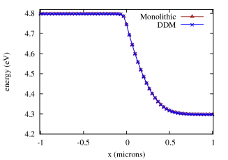
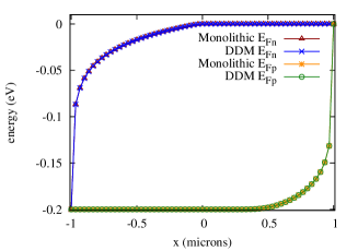
Our experiment is with silicon Si as the material in , with representing a doped region and an doped region. First we verify that the solver with DDM produces the same results as that of the monolithic solver, see Figure 9.
Next we discuss the performance of DDM. Table 3 shows that DDM is mesh-independent for both the potential and the current-continuity equations, and that the iteration counts do not vary between Gummel iterations for homojunction case. We note that the tolerance criteria are currently set the same as in Gummel iteration, and this could be changed in the future to avoid oversolving. We used in Algorithms (NN), (NNC), (NNC) , respectively.
| N | |||
|---|---|---|---|
| 1001–4001 | 2 | 5 | 6 |
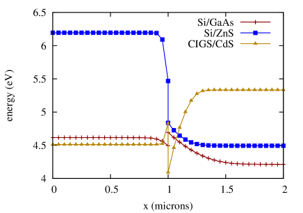
Heterojunction examples. We use three examples of interfaces: Si/GaAs, Si/ZnS, and CIGS/CdS. We apply DDM to the potential equation while the current-continuity equations are solved monolithically. Even though the potential equation is linear, the dependence of unknowns on is nonlinear. We are interested both in the qualitative results as well as in the performance of the algorithm as compared to the monolithic solver.
As seen in Figure 10, the heterojunction causes discontinuity in the potential, in a way specific to the particular interface considered. This is consistent with results shown in Sections 4.1, 4.2.
Next we discuss various computational aspects of the algorithm. In spite of highly varying coefficients and discontinuous solutions, we verify that DDM-solver and Algorithm (NNH) maintain the second order of accuracy as expected from FD method. In particular, at every step of Gummel iteration, its solution, e.g., that to the potential equation, should exhibit the same convergence order, i.e., second order, as that for any other self-adjoint elliptic equation, as long as the solutions are smooth enough.
To verify, a grid convergence test is performed. First the solver is run with a step size of , corresponding to computational nodes. The solver is then run for various coarser grids to check for order of convergence of to the fine grid solution. The error is shown in Table 4.
| observed order | ||
|---|---|---|
| 1002 | ||
| 2002 | 2.2275 | |
| 3002 | 2.1216 | |
| 4002 | 2.0012 |
Further, we check for mesh-independence which holds similarly to that for homojunction in Table 3, see Table 5.
| N | GI 1 | GI 2 | GI 3 | GI 4 | GI 5 |
|---|---|---|---|---|---|
| 1002-4002 | 7 | 6 | 4 | 2 | 1 |
The relaxation parameter affects the convergence of Algorithm (NN), and the optimal choice of is strongly influenced by material properties. In Table 6 this influence is shown through comparison of DDM iterations for different materials while the relaxation parameter is fixed. In particular, a relaxation parameter good for Si/ZnS has poor performance for Si/GaAs, and acceptable but sub-optimal performance for CIGS/CdS; these results correlate with the slope of the potential across the true interface region , see Figure 10. In Table 7 we show an optimal for each material determined by trial and error. In particular, optimal relaxation parameters for CIGS/CdS and Si/ZnS are much closer than those of Si/GaAs.
| Material | GI 1 | GI 2 | GI 3 | GI 4 | GI 5 | GI 6 | ||
|---|---|---|---|---|---|---|---|---|
| Si/ZnS | -0.63 | 0.005 | 9 | 11 | 10 | 8 | 5 | 2 |
| Si/GaAs | 0.2 | 0.005 | 225 | 283 | 143 | 21 | 1 | - |
| CIGS/CdS | -0.74 | 0.005 | 4 | 10 | 7 | 4 | 2 | 1 |
| Material | GI 1 | GI 2 | GI 3 | GI 4 | GI 5 | GI 6 | |
|---|---|---|---|---|---|---|---|
| Si/ZnS | 0.005 | 9 | 11 | 10 | 8 | 5 | 2 |
| Si/GaAs | 0.05 | 7 | 6 | 4 | 2 | 1 | - |
| CIGS/CdS | 0.0051 | 4 | 9 | 6 | 4 | 2 | 1 |
Next, we perform a study of sensitivity of performance of DDM to the value of . This is important since there may be a large margin of error in the computed or experimental values of . We test it for Si/GaAs; see Table 8 for behavior of the DDM for a wide range of . Overall, the method appears as robust as a Gummel iteration is for a given physical problem.
| GI 1 | GI 2 | GI 3 | GI 4 | GI 5 | |
|---|---|---|---|---|---|
| 0.0 | 8 | 14 | 7 | 1 | 1 |
| 0.1 | 5 | 9 | 6 | 1 | 1 |
| 0.2 | 5 | 6 | 4 | 2 | 1 |
| 0.3 | 7 | 6 | 5 | 2 | 1 |
| 0.4 | 8 | 9 | 6 | 3 | 1 |
| 0.5 | 8 | 7 | 5 | 3 | 1 |
Finally, we compare computational complexity of the monolithic and DDM solvers. Specifically, we study the number of Newton iterations depending on the discretization that a monolithic solver needs with that of subdomain solvers when using DDM. Note that the complexity of the monolithic solver is per each Gummel iteration, since we expect that the linear solver involving a Jacobian in each Newton iteration needs only operations due to the three-point stencil of FD discretization. On the other hand, the subdomain solvers need or operations, per Gummel iteration, and per each interface iteration in (133) in Algorithm (NNH). Since , unless the interface iteration (133) converges immediately or the subdomain solvers are executed in parallel, DDM is about times slower in the 1d case than a monolithic solver, which is well-known. At the same time, in 2d, for higher order schemes, or on multicore or multiprocessor environments, the computational complexity is in favor of DDM, especially for problems close to being out-of-core.
Still, an important fact is to verify whether is mesh independent for the heterojunction problem, since now the subdomain solvers may not necessarily react favorably to the progress of interface iteration. However, from Table 9 we see that the monolithic and DDM solvers are both mesh independent, and they perform similarly in that is not much worse for DDM than that for the monolithic solver.
| N | GI 1 | GI 2 | GI 3 | GI 4 | GI 5 | |
|---|---|---|---|---|---|---|
| monolithic | 1002-4002 | 3 | 6 | 3 | 2 | 1 |
| DDM | 1002-4002 | 3+3 | 6+5 | 3+5 | 2+5 | 1+5 |
Overall, the performance of DDM is promising for heterojunction, both in quality of the results and computational complexity. One of many advantages of DDM is that it can be applied to couple black-box single-material solvers across interfaces, and these solvers can be, in turn, optimized for single materials.
More studies on interface solver are needed, especially as it seems that it may be oversolving the problem in the first few Gummel iterations. Optimal parameters and preconditioners will be needed for 2d geometries.
5 Discussion and Conclusions
Numerical simulation of heterojunctions in semiconductor phenomena is an important tool in material science allowing for design, e.g., solar cells, and computational implementations in 1d of the basic heterojunction model have been in use in community and industry codes such as, e.g., ampsweb ; scapsweb . In this paper we emphasized the multiscale character of the problem, focused on its mathematical structure, and proposed a domain decomposition (DDM) algorithm. Our applications examples use data from a microscale computational model based on Density Functional Theory (DFT) which simulates phenomena in the interface region, and provides the crucial interface data for the macroscale model. In particular, the DFT model can provide data for materials that have been predicted but have not yet been synthesized and/or fully characterized.
The presentation of the coupled bulk subdomain plus heterojunction model in this paper provides a basis for future analyses, extensions and improvements. We outlined similarities to other models known from the literature on fluid flow models in domains with fractures and barriers or different fluid physics on each of the sides of an interface. There is substantial current interest in mathematical and computational literature for those problems, and some results may carry over to the heterojunction models. In particular, it is clear that an alternative to using node-centered discretizations, i.e., such as in mixed finite element methods, needs to be investigated. Mixed finite elements enforce continuity of fluxes naturally, and do not require doubling of interface unknowns. In fact, their use was successful for the fluid flow problems described above, and we plan to investigate their use in our future work.
The DDM algorithm that we proposed is promising: it decouples the interface calculations in each step of the Gummel loop from the subdomain calculations, similarly to how this is done in the Schur complement formulations. The algorithm makes it possible to use “black boxes” or “monolithic subdomain solvers” with constant material parameters, as long as they can use Dirichlet and/or flux boundary conditions. The algorithm converges easily for the potential equation, and for continuity equations for homojunctions. The algorithm for the continuity equation at heterojunctions is in progress. The DDM formulation can be naturally extended to 2d regions with complicated geometry of interfaces, or/and to materials with multiple heterojunctions. In contrast, such extensions may be very difficult for monolithic solvers in which interface equations are hard-coded. We plan to address 2d implementation as soon as all he theoretical and computational issues for the 1d case have been resolved.
Numerous extensions and refinements of our model are possible. These include the use of highly refined and adaptive grids based on a-posteriori finite-element error indicators and/or estimators, as well as rigorous formulations using other than finite difference approaches and the use of block-centered grids. Furthermore, for complicated 2D interfaces, one can consider the use of Immersed Interface methods (IMM). These have already been proposed for equations similar to the potential equation with nonhomogeneous jump in GongLiLi ; HeLinLin ; KwakCMAME , but it is not clear yet how they may be used for the nonlinear Robin-like condition.
Acknowledgments
We would like to thank National Science Foundation for supporting this research via NSF-DMS 1035513 grant "SOLAR: Enhanced Photovoltaic Efficiency through Heterojunction assisted Impact Ionization". We also thank Christopher Reidy and Janet Tate for providing us with the TEM image in Figure 2, and Angus Rockett for helpful discussions.
We also thank the anonymous referees for their suggestions which helped to improve the manuscript.
Appendix A Appendix
1.1 Material and environmental parameters
Unless otherwise stated, properties of the materials used in our calculations are shown in Table 10. The values are given in physical (unscaled) units. Table 11 gives parameters for particular interfaces or calculations. The subscripts and applied to and denote the narrow bandgap material and the wide bandgap material respectively. (By convention, the narrow bandgap material is listed first in the name of the interface; for example “Si/GaAs” implies that Si is the narrow bandgap material). The , , and quantities are defined by the appropriate property in the wide bandgap material minus this property in the narrow bandgap material.
| material | Si | ZnS | CIGS | CdS | GaAs |
|---|---|---|---|---|---|
| 11.9 Sze | 8.4 Sze | 13.5 minemoto01the | 10 gloeckler03num | 12.9 Sze | |
| (eV) | 4.27 (111) maierhofer91val | 3.17 (111) maierhofer91val | 4.35 minemoto01the | 4.79 swank67sur | 4.07 Sze |
| (eV) | 1.1 Sze | 3.54 maierhofer91val | 1.16 minemoto01the | 2.42 wei93ban | 1.42 Sze |
| (cm-3) | Sze | ruda92book | gloeckler03num | gloeckler03num | Sze |
| (cm-3) | Sze | ruda92book | gloeckler03num | gloeckler03num | Sze |
| (cm2/s) | 37.6 Sze | 15.5 Sze | 2.6 gloeckler03num | 2.6 gloeckler03num | 207 Sze |
| (cm2/s) | 12.9 Sze | 1.0 seeger10book | 0.65 gloeckler03num | 0.65 gloeckler03num | 5.2 Sze |
| SRH (s) | gloeckler03num | gloeckler03num | |||
| SRH (s) | gloeckler03num | gloeckler03num | |||
| (cm3/s) |
| interface | Si/ZnS | CIGS/CdS | Si/GaAs | Si/Si |
|---|---|---|---|---|
| () (A cm-2) | ||||
| () (A cm-2) | ||||
| (cm-3) | ||||
| (cm-3) | ||||
| (cm-3s-1) | 0, | |||
| (cm-3s-1) | 0, | |||
| (eV) | , | 0 | ||
| (eV) | , | gloeckler03num | 0 | |
| (eV) | , | 0 |
The Shockley-Read-Hall (SRH) recombination lifetimes, and , are highly dependent on dopant density and growth conditions. In our Si/ZnS simulations we set the SRH lifetimes for Si and ZnS to s.
The SRH lifetime values for the CIGS/CdS calculations are based on Ref. gloeckler03num , which gives parameters used by M. Gloeckler to establish a baseline model for a CIGS/CdS/ZnO solar cell. The parameters reflect alteration from pure material characteristics both by the presence of high dopant density (), as well as by the growth processes used to create layered thin-film solar cells.
The values are estimated according to whether the material has an electronic structure property known as a direct gap. Direct materials are given a value of cm3/s while indirect materials are given a value of cm3/s Sze .
values for Si and ZnS are calculated from effective mass data in the cited reference using the convention that the lower energy “split off” hole band Sze is neglected. (An exception occurs for the Si/GaAs interface, for which we have used the approximation cm3 for Si, and for which and for GaAs are taken directly from values given in Appendix G of Ref. Sze .)
The values for and given here are typically calculated from data giving the mobilities and , according to
| (134) |
with the analogous equation for and .
For the Si/GaAs calculations, we have used the Si electron affinity value eV Sze , which is not specific to a particular crystal direction. In these calculations we have also used s for both Si and GaAs and neglected direct recombination ().
The effective Richardson’s constants and are estimated Sze from and according to
| (135) | |||||
| (136) |
where K.
The values shown in Table 11 for the Si/ZnS interface indicate both thermal equilibrium and illuminated () calculations, while the offsets shown correspond to experiment maierhofer91val (first value) and the DFT calculations (second value).
In all simulations, the recombination velocities defined in Section 3.2 are given values between and cm/s, as these velocities are typically less than or approximately equal to the average (thermal) electron velocity of about cm/s.
1.2 Scaling for the continuum model
The dimensionless quantities using in the model formulated in Section 3 must generally be multiplied by appropriately dimensioned scaling constants. Our scaling in many respects follows that of Selber .
For charge densities such as , , , and , it is conventional to use as physical units the number of individual carriers or atoms per cubic centimeter, or simply cm-3. It is thus convenient to choose a scaling constant such as
| (137) |
or to use scaling based on or and . This simple definition of the dimensionless quantities , etc. will lead to a formal modification of the Poisson equation as given in (13). (Equation (13) omits constants for simplicity but requires a less intuitive scaling for the charge densities.)
The potential variables such as and can play a dual role as both scaled electrostatic potential quantities and as scaled energies of single charge carriers. Properly, is an electrostatic potential, originally in Volts (V), scaled by the thermal energy divided by the electronic charge (potential = energy / charge). eV/K is the Boltzmann constant and is the absolute temperature in Kelvins. In calculations we use K to approximate room temperature. The electronic charge is the positive elementary unit of charge; the charge of an electron is . The electron Volt, eV, is an energy equal to the electronic charge multiplied by 1 Volt. Physically, an electron (hole) in a region of potential 5 V has electrostatic energy eV ( eV). We define the scaling constant
| (138) | |||||
The dimensionless can be multiplied by to obtain the physical voltage, and a change in applied voltage of V at boundary corresponds to a change of eV / in the dimensionless quantity . To obtain the energies of electrons and holes in the conduction and valence bands, we multiply physical potential quantities such as by . When these energies are expressed in eV, the multiplication above does not change the numerical value, and thus the value of can also be thought of as the value of the energy scale .
Using the scaling above, the electrostatic Poisson equation represented by (13) requires a factor involving the physical constants C/(V cm), the permittivity of free space, and the electronic charge C, where C denotes Coulomb, the SI unit of charge. The Poisson equation for the scaling described above is thus
| (139) |
where the variables , , , and are dimensionless, is expressed in Coulombs, and is an optional distance scaling factor in cm. We have used
| (140) |
We use a scaling factor to make and dimensionless,
| (141) |
The result of the scaling of and is that time is scaled. For example the SRH recombination constants are scaled by
The dimensionless mobilities have been scaled by .
An important quantity is the physical current density which is given in A/cm). The resulting scaling factor for current densities is
| (142) |
where is in Coulombs.
Scaling of the remaining quantities used in the continuum model can be derived in terms of the above scaling constants by inspection of the equations that use and/or define them.
1.3 Equivalence of transmission conditions to the algebraic DDM formulation via second order finite differences
Here we show that with proper discretization of interface condition expressing continuity of fluxes as in the transmission condition (41) we obtain the algebraic system (94). The argument presented below also works for the heterojunction system (107).
First, assume that the material constants are not the same on both sides of the interface which accounts later for the case of heterojunction.
We note that a one-sided approximation at the interface is only first order accurate, and a similar approximation together with (41) result in
| (143) |
thus do not allow any charges at , and lead to an inaccurate solution.
A second order approximation introduces an additional “ghost” unknown , which can be eliminated using a discretization of (13) that would be posed at , i.e., (60) for
| (144) |
Similarly, for an approximation to we have
| (145) |
From (41) we have, using these approximations, that
and multiplying by we get
| (146) |
Adding (144)-(146), and dividing by eliminates the ghost unknowns , and we obtain
| (147) |
which is a proper discretization of (44).
1.4 Schur complement form for heterojunction
Here we show details leading to (109), (110). We rewrite (107) to see that it gives the four equations
| (148) | |||||
| (149) | |||||
| (150) | |||||
| (151) |
Using (151) in (149)-(150) we obtain:
| (152) | |||||
| (153) |
Now we use these and (148) to solve for and ,
| (154) | |||
| (155) |
Substituting (154) and (155) into (153) then gives us with given by (109) and given by (110).
References
- (1) D. H. Foster, V. Jieratum, R. Kykyneshi, D. A. Keszler, and G. Schneider, “Electronic and optical properties of potential solar absorber Cu3PSe4”, Applied Physics Letters 99(18), pp. 181903–181903–3 (2011).
- (2) Vorranutch Itthibenchapong, Robert S. Kokenyesi, Andrew J. Ritenour, Lev N. Zakharov, Shannon W. Boettcher, John F. Wager, and Douglas A. Keszler, “Earth-abundant cu-based chalcogenide semiconductors as photovoltaic absorbers”, Journal of Materials Chemistry C 1(4), pp. 657–662 (2012).
- (3) Victor I. Klimov, “Spectral and dynamical properties of multiexcitons in semiconductor nanocrystals”, (2007).
- (4) Nathaniel M. Gabor, Zhaohui Zhong, Ken Bosnick, Jiwoong Park, and Paul L. McEuen, “Extremely efficient multiple electron-hole pair generation in carbon nanotube photodiodes”, Science 325(5946), pp. 1367 –1371 (2009).
- (5) Justin B. Sambur, Thomas Novet, and B. A. Parkinson, “Multiple exciton collection in a sensitized photovoltaic system”, Science 330(6000), pp. 63 –66 (2010).
- (6) C. Reidy and J. Tate, in preparation.
- (7) S. Selberherr, Analysis and Simulation of Semiconductor Devices, Springer-Verlag (1984).
- (8) Peter A. Markowich, The stationary semiconductor device equations, Computational Microelectronics. Springer-Verlag Vienna (1986).
- (9) P. A. Markowich, C. A. Ringhofer, and C. Schmeiser, Semiconductor equations, Springer-Verlag Vienna (1990).
- (10) Randolph E. Bank, Donald J. Rose, and Wolfgang Fichtner, “Numerical methods for semiconductor device simulation”, SIAM J. Sci. Statist. Comput. 4(3), pp. 416–435 (1983).
- (11) Joseph W. Jerome, Analysis of charge transport, Springer-Verlag Berlin (1996).
- (12) Carlo de Falco, Joseph W. Jerome, and Riccardo Sacco, “Quantum-corrected drift-diffusion models: solution fixed point map and finite element approximation”, J. Comput. Phys. 228(5), pp. 1770–1789 (2009).
- (13) M. A. Green, Third Generation Photovoltaics: Advanced Solar Energy Conversion /, Springer-Verlag Berlin Heidelberg, Berlin, Heidelberg : (2006).
- (14) Massimo V. Fischetti and Steven E. Laux, “Monte carlo analysis of electron transport in small semiconductor devices including band-structure and space-charge effects”, Phys. Rev. B 38, pp. 9721–9745 (1988).
- (15) Marco Saraniti, Shela Aboud, Julien Branlard, and StephenM. Goodnick, “Particle-based simulation: An algorithmic perspective”, Journal of Computational Electronics 5(4), pp. 405–410 (2006).
- (16) José A. Carrillo, Irene M. Gamba, Armando Majorana, and Chi-Wang Shu, “2D semiconductor device simulations by WENO-Boltzmann schemes: efficiency, boundary conditions and comparison to Monte Carlo methods”, J. Comput. Phys. 214(1), pp. 55–80 (2006).
- (17) Chris G. Van de Walle and Richard M. Martin, “Theoretical calculations of heterojunction discontinuities in the Si/Ge system”, Physical Review B 34(8), pp. 5621 (1986).
- (18) Kyounghoon Yang, Jack R East, and George I. Haddad, “Numerical modeling of abrupt heterojunctions using a thermionic-field emission boundary condition”, Solid-State Electronics 36, pp. 321–330 (1993).
- (19) K. Horio and H. Yanai, “Numerical modeling of heterojunctions including the thermionic emission mechanism at the heterojunction interface”, IEEE Trans. Electron Devices ED-37, pp. 1093–1098 (1990).
- (20) “Amps1d analysis of Microelectronic and Photonic Structures”, http://www.ampsmodeling.org.
- (21) M. Burgelman, P. Nollet, and S. Degrave, “Modelling polycrystalline semiconductor solar cells”, Thin Solid Films 361-362, pp. 527–532 (2000).
- (22) “Simulation programme SCAPS-1D for thin film solar cells developed at ELIS, University of Gent”, http://users.elis.ugent.be/ELISgroups/solar/projects/scaps.html.
- (23) Stephen J. Fonash, “Band structure and photocurrent collection in crystalline and polycrystalline p-n heterojunction solar cells”, Solid-State Electronics 22(10), pp. 907 – 910 (1979).
- (24) Alfio Quarteroni and Alberto Valli, Domain decomposition methods for partial differential equations, Numerical Mathematics and Scientific Computation. The Clarendon Press Oxford University Press New York (1999), Oxford Science Publications.
- (25) Fernando Morales and R. E. Showalter, “The narrow fracture approximation by channeled flow”, J. Math. Anal. Appl. 365(1), pp. 320–331 (2010).
- (26) Fernando Morales and Ralph E. Showalter, “Interface approximation of Darcy flow in a narrow channel”, Math. Methods Appl. Sci. 35(2), pp. 182–195 (2012).
- (27) Vincent Martin, Jérôme Jaffré, and Jean E. Roberts, “Modeling fractures and barriers as interfaces for flow in porous media”, SIAM J. Sci. Comput. 26(5), pp. 1667–1691 (electronic) (2005).
- (28) Ali Saada N. Frih, Jean E. Roberts, “Modeling fractures as interfaces: A model for Forchheimer fractures”, Computational Geosciences 2 (2008).
- (29) Vivette Girault, Béatrice Rivière, and Mary F. Wheeler, “A discontinuous Galerkin method with nonoverlapping domain decomposition for the Stokes and Navier-Stokes problems”, Math. Comp. 74(249), pp. 53–84 (electronic) (2005).
- (30) Vivette Girault and Béatrice Rivière, “DG approximation of coupled Navier-Stokes and Darcy equations by Beaver-Joseph-Saffman interface condition”, SIAM J. Numer. Anal. 47(3), pp. 2052–2089 (2009).
- (31) G. Kanschat and B. Rivière, “A strongly conservative finite element method for the coupling of Stokes and Darcy flow”, J. Comput. Phys. 229(17), pp. 5933–5943 (2010).
- (32) Aycil Cesmelioglu and Béatrice Rivière, “Existence of a weak solution for the fully coupled Navier-Stokes/Darcy-transport problem”, J. Differential Equations 252(7), pp. 4138–4175 (2012).
- (33) P. Hohenberg and W. Kohn, “Inhomogeneous electron gas”, Physical Review 136(3B), pp. B864–B871 (1964).
- (34) W. Kohn and L. J. Sham, “Self-consistent equations including exchange and correlation effects”, Physical Review 140(4A), pp. A1133–A1138 (1965).
- (35) John P. Perdew and Stefan Kurth, “Density functionals for non-relativistic Coulomb systems in the new century”, In Carlos Fiolhais, Fernando Nogueira, and Miguel A.L. Marques, editors, A Primer in Density Functional Theory volume 620 of Lecture Notes in Physics , pp. 1–55. Springer Berlin Heidelberg (2003).
- (36) C. Fiolhais, F. Nogueira, and Miguel A. L Marques, A primer in density functional theory, Springer Berlin; New York (2003).
- (37) Eberhard Engel and Reiner M Dreizler, Density functional theory an advanced course, Springer Berlin; Heidelberg; New York (2011).
- (38) Albert Messiah, Quantum Mechanics: Two Volumes Bound as One, Dover Mineola, New York (1999).
- (39) Mel Levy, “Universal variational functionals of electron densities, first-order density matrices, and natural spin-orbitals and solution of the v-representability problem”, Proceedings of the National Academy of Sciences 76(12), pp. 6062–6065 (1979), PMID: 16592733.
- (40) Elliott H. Lieb, “Density functionals for coulomb systems”, International Journal of Quantum Chemistry 24(3), pp. 243–277 (1983).
- (41) U. von Barth and L. Hedin, “A local exchange-correlation potential for the spin polarized case. i”, Journal of Physics C: Solid State Physics 5(13), pp. 1629 (1972).
- (42) J. P. Perdew and Alex Zunger, “Self-interaction correction to density-functional approximations for many-electron systems”, Physical Review B 23(10), pp. 5048–5079 (1981).
- (43) L. J. Sham and M. Schlüter, “Density-functional theory of the energy gap”, Physical Review Letters 51(20), pp. 1888–1891 (1983).
- (44) M. Shishkin and G. Kresse, “Self-consistent GW calculations for semiconductors and insulators”, Physical Review B (Condensed Matter and Materials Physics) 75(23), pp. 235102–9 (2007).
- (45) Chris G. Van de Walle and Richard M. Martin, ““Absolute” deformation potentials: Formulation and ab initio calculations for semiconductors”, Physical Review Letters 62(17), pp. 2028 (1989).
- (46) P. A. Markowich, C. A. Ringhofer, and C. Schmeiser, Semiconductor equations, Springer-Verlag Vienna (1990).
- (47) Simon Sze and Kwok Ng, Physics of Semiconductor Devices, Wiley-Interscience (2006).
- (48) Béatrice Rivière, Discontinuous Galerkin methods for solving elliptic and parabolic equations, Volume 35 of Frontiers in Applied Mathematics, Society for Industrial and Applied Mathematics (SIAM) Philadelphia, PA (2008).
- (49) R. E. Showalter, Hilbert space methods for partial differential equations, Electronic Monographs in Differential Equations San Marcos, TX (1994), Electronic reprint of the 1977 original.
- (50) Franco Brezzi and Michel Fortin, Mixed and hybrid finite element methods volume 15 of Springer Series in Computational Mathematics, Springer-Verlag New York (1991).
- (51) Zhangxin Chen and Bernardo Cockburn, “Error estimates for a finite element method for the drift-diffusion semiconductor device equations”, SIAM J. Numer. Anal. 31(4), pp. 1062–1089 (1994).
- (52) Zhangxin Chen and Bernardo Cockburn, “Analysis of a finite element method for the drift-diffusion semiconductor device equations: the multidimensional case”, Numer. Math. 71(1), pp. 1–28 (1995).
- (53) T. F. Russell and M. F. Wheeler, “Finite element and finite difference methods for continuous flows in porous media”, In R. E. Ewing, editor, The Mathematics of Reservoir Simulation , pp. 35–106. SIAM Philadelphia (1983).
- (54) R. Glowinski and M. F. Wheeler, “Domain decomposition and mixed finite element methods for elliptic problems”, In R. Glowinski, G. H. Golub, G. A. Meurant, and J. Periaux, editors, First International Symposium on Domain Decomposition Methods for Partial Differential Equations , pp. 144–172. SIAM, Philadelphia (1988).
- (55) T. Arbogast, L. C. Cowsar, M. F. Wheeler, and I. Yotov, “Mixed finite element methods on non-matching multiblock grids”, SIAM J. Numer. Anal. 37, pp. 1295–1315 (2000).
- (56) M. Peszyńska, “Advanced techniques and algorithms for reservoir simulation III. Multiphysics coupling for two phase flow in degenerate conditions”, In J. Chadam, A. Cunningham, R. E. Ewing, P. Ortoleva, and M. F. Wheeler, editors, IMA Volume 131: Resource Recovery, Confinement, and Remediation of Environmental Hazards , pp. 21–40. Springer (2002).
- (57) Ivan Yotov, “Advanced techniques and algorithms for reservoir simulation. IV. Multiblock solvers and preconditioners”, In Resource recovery, confinement, and remediation of environmental hazards (Minneapolis, MN, 2000) volume 131 of IMA Vol. Math. Appl. , pp. 41–55. Springer New York (2002).
- (58) Randall J. LeVeque, Finite difference methods for ordinary and partial differential equations, Society for Industrial and Applied Mathematics (SIAM) Philadelphia, PA (2007), Steady-state and time-dependent problems.
- (59) Yan Gong, Bo Li, and Zhilin Li, “Immersed-interface finite-element methods for elliptic interface problems with nonhomogeneous jump conditions”, SIAM J. Numer. Anal. 46(1), pp. 472–495 (2007/08).
- (60) Kwang S. Chang and D. Y. Kwak, “Discontinuous bubble scheme for elliptic problems with jumps in the solution”, Comput. Methods Appl. Mech. Engrg. 200(5-8), pp. 494–508 (2011).
- (61) Xiaoming He, Tao Lin, and Yanping Lin, “Immersed finite element methods for elliptic interface problems with non-homogeneous jump conditions”, Int. J. Numer. Anal. Model. 8(2), pp. 284–301 (2011).
- (62) C. Bernardi, Y. Maday, and A. T. Patera, “A new nonconforming approach to domain decomposition: the mortar element method”, In Nonlinear partial differential equations and their applications. Collège de France Seminar, Vol. XI (Paris, 1989–1991) volume 299 of Pitman Res. Notes Math. Ser. , pp. 13–51. Longman Sci. Tech. Harlow (1994).
- (63) Małgorzata Peszyńska, Mary F. Wheeler, and Ivan Yotov, “Mortar upscaling for multiphase flow in porous media”, Comput. Geosci. 6(1), pp. 73–100 (2002).
- (64) Q. Lu, M. Peszyńska, and M. F. Wheeler, “A parallel multi-block black-oil model in multi-model implementation.”, SPE Journal 7(3), pp. 278–287 (2002), SPE 79535.
- (65) Paul T. Lin, John N. Shadid, Marzio Sala, Raymond S. Tuminaro, Gary L. Hennigan, and Robert J. Hoekstra, “Performance of a parallel algebraic multilevel preconditioner for stabilized finite element semiconductor device modeling”, J. Comput. Phys. 228(17), pp. 6250–6267 (2009).
- (66) W. A. Harrison, E. A. Kraut, J. R. Waldrop, and R. W. Grant, “Polar heterojunction interfaces”, Physical Review B 18(8), pp. 4402–4410 (1978).
- (67) Naoyuki Nakagawa, Harold Y. Hwang, and David A. Muller, “Why some interfaces cannot be sharp”, Nature Materials 5(3), pp. 204–209 (2006).
- (68) D. H. Foster and G. Schneider, in preparation.
- (69) Ch. Maierhofer, “Valence band offset in ZnS layers on Si(111) grown by molecular beam epitaxy”, Journal of Vacuum Science & Technology B: Microelectronics and Nanometer Structures 9(4), pp. 2238 (1991).
- (70) Takashi Minemoto, Takuya Matsui, Hideyuki Takakura, Yoshihiro Hamakawa, Takayuki Negami, Yasuhiro Hashimoto, Takeshi Uenoyama, and Masatoshi Kitagawa, “Theoretical analysis of the effect of conduction band offset of window/CIS layers on performance of CIS solar cells using device simulation”, Solar Energy Materials and Solar Cells 67(1–4), pp. 83–88 (2001).
- (71) M. Gloeckler, “CIGS Gloeckler baseline-Solar Cells Simulation-University of Illinois-Engineering Wiki”, https://wiki.engr.illinois.edu/display/solarcellsim/CIGS.
- (72) Su-Huai Wei and Alex Zunger, “Band offsets at the CdS/CuInSe2 heterojunction”, Applied Physics Letters 63(18), pp. 2549–2551 (1993).
- (73) Robert K. Swank, “Surface properties of II-VI compounds”, Physical Review 153(3), pp. 844–849 (1967).
- (74) H. E. Ruda, editor, Widegap II-VI Compounds for Opto-electronic Applications, Chapman & Hall (1992).
- (75) Karlheinz Seeger, Semiconductor Physics: An Introduction, 9th Edition, Springer Berlin (2010).