Heteroepitaxy of Group IV-VI Nitrides by Atomic Layer Deposition
Abstract
Heteroepitaxial growth of selected group IV-VI nitrides on various orientations of sapphire (-Al2O3) is demonstrated using atomic layer deposition. High quality, epitaxial films are produced at significantly lower temperatures than required by conventional deposition methods. Characterization of electrical and superconducting properties of epitaxial films reveals a reduced room temperature resistivity and increased residual resistance ratio (RRR) for films deposited on sapphire compared to polycrystalline samples deposited concurrently on fused quartz substrates.
Transition metal nitrides exhibit a host of rich physics and functionality ranging from superconductivity to applications as refractory coatings.Toth (1971) There is significant interest in epitaxial nitrides since epitaxy-induced changes in the crystallinity and morphology of thin films can influence both fundamental materials properties and device performance. Heteroepitaxial growth of MoN, NbN, and TiN has been explored by several methods, including reactive sputtering,Noskov et al. (1980); Lloyd et al. (2001); Espiau de Lamaëstre, Odier, and Villégier (2007) pulsed laser deposition (PLD),Talyansky et al. (1998) chemical vapor deposition (CVD),Wang et al. (1996) and polymer assisted deposition (PAD).Zhang et al. (2011); *luo_mon_pad_2011; Zou et al. (2008) Atomic layer deposition (ALD), which utilizes sequential self-limiting surface chemical reactions to deposit material in a layer-by-layer mode,Ritala and Leskelä (2001); Puurunen (2005) offers several advantages over traditional growth techniques. ALD provides atomic-scale uniformity over large areas, unmatched conformality over complex-shaped substrates, and deposition temperatures well below those typically required by other methods.
While the ALD of metal nitrides is known to result in the formation of crystalline films in many cases,Miikkulainen et al. (2013) little attention has been devoted to the investigation of heteroepitaxial growth on suitable single crystal substrates. Several groups have reported epitaxial ALD of AlN,Asif Khan et al. (1992a) GaN,Asif Khan et al. (1992b); *khan_sensors_1992; *khan_super_1993; *karam_gan_1995, InN,Nepal et al. (2013) and InxGa1-xNBedair et al. (1997) films on sapphire (-Al2O3) from organometallic precursors. Epitaxial GaN has also been reported on (111)GaAs using a chloride-ammonia process.Tsuchiya et al. (1996) However, apart from the group III nitrides, epitaxy of nitrides has been entirely unexplored in the ALD literature despite a large volume of studies concerning transition metal nitride ALD.Miikkulainen et al. (2013); Kim (2003) In this letter we report the ALD of epitaxial MoN, NbN, NbxTi1-xN, and TiN films on c-, m-, a-, and r-plane sapphire. Heteroepitaxial orientations were determined by x-ray diffraction (XRD) and the effects of substrate induced epitaxy on film resistivity and superconductivity are discussed. While several studies have examined superconductivity in ALD films, Proslier et al. (2011a); *klug_nbc_2011; *proslier_ecs_2011; *driessen_prl_2012; *coumou_tin_2013 the effects of crystallinity on film properties have thusfar not been reported.
ALD film growth was carried out in a custom-built hot-walled viscous flow reactor similar to that described elsewhere.Elam, Groner, and George (2002) During ALD, a 360 sccm flow of UHP N2 at 1.0 Torr served as purge and carrier gas. Prior to ALD, all substrates were cleaned via sonication in acetone, isopropanol, and deionized water. Nitride films were deposited at 450C using metal chlorides (TiCl4, NbCl5, and MoCl5) and ammonia (NH3) as precursors. NbxTi1-xN samples were deposited using alternating TiN and NbN ALD cycles to achieve a desired composition. For these samples metallic Zn was used as an additional reactant for the reduction of the metal chlorides.Ritala et al. (1997) X-ray diffraction (XRD) and x-ray reflectivity (XRR) were performed with a Philips X’Pert MRD diffractometer using Cu K radiation ( Å) and operated at 30 kV / 30 mA. Incident x-ray beam conditioning was provided by a 60 mm graded parabolic W/Si mirror with a 0.8∘ acceptance angle and a 1/32∘ divergence slit. The reflected beam was collected with a sealed proportional detector positioned behind a 0.27∘ parallel plate collimator and a pyrolytic graphite monochromator. Electrical resistivity down to 1.3 K was obtained via a four terminal measurement in a custom-built apparatus.
The epitaxial orientations determined by XRD for a series of MoN, NbN, TiN, and Nb0.8Ti0.2N samples are summarized in Table 1. For clarity, planes and directions for MoN and Al2O3 are described using the four-axis hexagonal reference basis.Otte and Crocker (1965) In all cases, films grown on sapphire were epitaxial while those grown concurrently on (001)Si and fused quartz (G.E. 124) substrates were polycrystalline. At least two twin variants were detected for all samples except the cases of MoN grown on c- or m-plane Al2O3.
Specular and off-specular XRD scans of an 80 nm thick MoN film deposited on c-Al2O3 are shown in Fig. 1(a) and 1(b), respectively. A single -MoN orientation was observed, (0001)MoN(0001)Al2O3, which is consistent with the results reported for MoN/c-Al2O3 prepared at 900∘ by PAD.Zhang et al. (2011); *luo_mon_pad_2011 From analysis of the (0002) and {202} film reflections, the out-of-plane (OP) mosaic and in-plane (IP) texture of the MoN film were and , respectively (FWHM). A broad peak corresponding to the (111) reflection of cubic -Mo2N was observed with approximately 1/120 the integrated intensity of the MoN(0002) peak. This is consistent with a thin -Mo2N layer at the film-substrate interface as observed in polycrystalline films deposited on AlN/quartz.sup Roughness of the thicker MoN layer ( nm) prevented accurate determination of the Mo2N layer thickness by x-ray reflectivity. However, the width of the (111) peak established a lower limit of nm on the Mo2N thickness. The FWHM of the -Mo2N(111) x-ray rocking curve was ,sup indicating that the Mo-rich layer is highly-ordered, although the IP orientation of this thin layer was not investigated due to practical limitations of the x-ray source. The same epitaxial relationship was obtained when MoN was deposited on c-Al2O3 with an ALD-grown 6 nm thick epitaxial (0001)AlN buffer layer.
| Film | Substrate | Epitaxial relationship |
|---|---|---|
| MoN | c-Al2O3 | (0001)MoN(0001)Al2O3 |
| NbN | c-Al2O3 | NbNAl2O3 |
| NbNAl2O3 | ||
| TiN | c-Al2O3 | TiNAl2O3 |
| TiNAl2O3 | ||
| MoN | m-Al2O3 | MoNAl2O3 |
| Nb0.8Ti0.2N | a-Al2O3 | Nb0.8Ti0.2NAl2O3 |
| Nb0.8Ti0.2NAl2O3 | ||
| Nb0.8Ti0.2NAl2O3 | ||
| Nb0.8Ti0.2NAl2O3 | ||
| MoN | r-Al2O3 | MoNAl2O3 |
| MoNAl2O3 | ||
| TiN | r-Al2O3 | TiNAl2O3 |
| TiNAl2O3 |
ALD of NbN and TiN on c-Al2O3 resulted in cubic (111)-oriented films with two twin IP variants in agreement with previous studies of sputtered NbNLloyd et al. (2001); Noskov et al. (1980) and PLD-grown TiN films.Talyansky et al. (1998) The XRD results obtained for a 20 nm thick TiN film are shown in Figs. 1(c) and 1(d). The six TiN{200} peaks observed in Fig. 1(d) indicate the presence of two twin domains related by a 180∘ rotation about the [111] axis. This leads to a doubling of the expected threefold rotational symmetry about the [111] axis and mirrors the symmetry of the Al2O3 basal plane. The IP epitaxial relationship can therefore be described as TiNAl2O3. The FWHM of the TiN(111) x-ray rocking curvesup was which indicates a significantly higher degree of OP alignment compared to the MoN/c-Al2O3 sample. The reduced OP mosaicity of the TiN film may be related to the lack of a secondary phase at the film-substrate interface. However, analysis of the {200} scan [Fig. 1(d)] indicates a broader IP texture (FWHM) compared to that of the MoN/c-Al2O3 sample which is likely a consequence of the twinned TiN microstructure. Identical measurements of a 35 nm thick film of the isostructural NbN found an analogous result.sup The OP mosaic and IP texture of the NbN film were and , respectively.
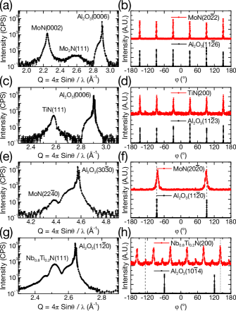
The XRD results obtained for a 50 nm thick MoN film grown on m-Al2O3 are presented in Figs. 1(e) and 1(f). The film is untwinned -MoN with a single orientation described by MoNAl2O3 and no evidence of a cubic phase. The relative orientations of MoN and Al2O3 are approximately equivalent to the c-Al2O3 case, with the hexagonal basal planes of film and substrate roughly parallel and the unit cell basis vectors offset by about the principal c-axis. However, Fig 1(f) reveals that the MoN peak centers are shifted along the azimuthal axis in opposite directions relative to each corresponding Al2O3 reflection. This is consistent with a tilting of the MoN(110) plane away from the Al2O3(100) by about the MoN[] axis. A rocking curve measurementsup of the MoN(220) reflection yielded a FWHM of indicating an OP mosaic comparable to the MoN/c-Al2O3 sample. However, the azimuthal widths of the (200) and (020) MoN peaks were , indicating a considerably wider variation in IP texture. While numerous factors can influence film microstructure, such as differing modes of interfacial strain relaxation, the broadened IP alignment is not surprising given the lower symmetry of the MoN(110) and Al2O3(100) planes compared to the high-symmetry (0001) planes.
On a-Al2O3, ALD of a 15 nm thick film of Nb0.8Ti0.2N resulted in a cubic (111)-oriented film with two sets of twinned IP domains similar to the case of NbN/a-Al2O3 reported in Ref. Lloyd et al., 2001. Fig. 1(g) demonstrates OP orientation of the film, with only Nb0.8Ti0.2N(111) and Al2O3(110) reflections observed in a specular XRD scan. In contrast, the azimuthal scans shown in 1(h) revealed the presence of twelve equally-spaced Nb0.8Ti0.2N{200} peaks rather than the three expected from a single crystallographic domain. The twelve observed {200} peaks comprise two distinct sets which are offset by 30∘ () and differ in integrated intensity by a factor of . This indicates that the film contains primary and secondary pairs of 180∘ twin IP domains which are offset by 90∘ about the [111] axis. The IP orientations of the primary and secondary sets of twins were determined by comparison with a scan through the Al2O3(104) and (01) reflections [Fig. 1(h)]. The orthogonal IP substrate directions and [0001] are oriented and , respectively, from the projection of the (104) in the Al2O3(110) plane. Since the directions are offset 30∘ from the projection of the in the (111) plane, the IP orientations of the primary and secondary twins are therefore described by Nb0.8Ti0.2NAl2O3 and Nb0.8Ti0.2NAl2O3, respectively. The OP mosaic and IP texture of the Nb0.8Ti0.2N film were and .
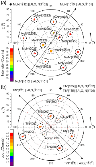
On r-Al2O3, the growth directions of both hexagonal MoN and cubic TiN are such that no allowed reflections are positioned along the specular Al2O3(102) rod. Consequently, x-ray pole figures of the MoN{202} and TiN{200} reflections were measured [Figs. 2(a) and 2(b), respectively] to determine film orientation in each case. Twelve MoN{202} peaks were observed for an 80 nm thick MoN/r-Al2O3 film, as shown in Fig. 2(a). Analysis of the data found that the film is [112]-oriented, with two IP twin variants related by a 180∘ rotation about the OP MoN[112] axis. For clarity, reflections from the two twins are labeled MoNa and MoNb in Fig. 2(a). Comparison with a scan through the Al2O3(23) and (113) reflections (not shown) was used to determine the IP epitaxial orientation of the film, which is described by MoNAl2O3. Small displacements of the MoN peaks from their symmetric postions indicate that the [112] directions of the film domains are tilted from Al2O3(102) by .
The TiN{200} x-ray pole figure obtained for a 20 nm TiN/r-Al2O3 sample is shown in Fig. 2(b). Six film peaks were observed indicating the presence of two twin variants TiNAl2O3 related by a 180∘ rotation about the IP TiN[] axis (or, equivalently, 180∘ rotations about both the OP [135] and IP [11] axes). In Fig. 2(b), peaks from the (135)- and ()-oriented domains are labeled TiNa and TiNb, respectively. The observed structure was equivalent to that reported for sputtered NbN on r-Al2O3.Noskov et al. (1980); Espiau de Lamaëstre, Odier, and Villégier (2007) The and peaks from the Al2O3 substrate were visible in the TiN{200} pole figure due to the small difference in d-spacing between the TiN and Al2O3 reflections (2.1209 Å and 2.0853 Å, respectively), and conveniently illustrate the orientational registry of the film and substrate.
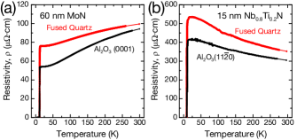
A comparison of electrical transport measurements of epitaxial and polycrystalline films found consistently more metallic behavior above the superconducting in films deposited on sapphire with relatively minor change in . Figs. 3(a) and 3(b) show the film resistivity, , measured for two different cases, respectively: a relatively thick 60 nm MoN film deposited on fused quartz and c-Al2O3 and a thin 15 nm Nb0.8Ti0.2N film deposited on quartz and a-Al2O3. In both cases, the critical temperature, , of the film on sapphire was % higher than the film on fused quartz. However, for 60 nm MoN, the room temperature resistivity, is % lower and the residual resistance ratio (RRR) () is % higher for the film grown on sapphire compared to the film on fused quartz. Likewise, for 15 nm Nb0.8Ti0.2N, and RRR for the sapphire sample were % lower and % higher, respectively, compared to the quartz sample. A similar effect was observed in Ref. Espiau de Lamaëstre, Odier, and Villégier, 2007 where a comparison of ultrathin twinned and untwinned NbN films found that while the presence of twinning resulted in 15% and a 20% lower RRR (), the was reduced by %.
In summary, high quality epitaxial films of MoN, NbN, TiN, and NbxTi1-xN were prepared on sapphire substrates by ALD at a low growth temperature of 450C. Observed orientations of MoN, NbN, and TiN deposited on c-Al2O3, and NbxTi1-xN on a-Al2O3 were consistent with prior literature. Untwinned (110)MoN was grown on m-Al2O3, while on r-Al2O3 both (135)TiN and [112]MoN grow with two IP twin domains. Epitaxial films were found to be more metallic than polycrystalline samples deposited concurrently on fused quartz. These results demonstrate the utility of ALD for the synthesis of epitaxial films of transition metal nitrides. This has significant implications for applications of nitride thin films where high crystalline quality is required in combination with moderate growth temperature, large-scale uniformity, precise thickness control, or conformal coating over complex-shaped surfaces.
This work was supported by the U.S. Department of Energy, Office of Science under contract No. DE-AC02-06CH11357. We thank J. D. Emery for his critical reading of our manuscript.
References
- Toth (1971) L. E. Toth, Transition Metal Carbides and Nitrides (Academic Press, New York, 1971).
- Noskov et al. (1980) V. L. Noskov, Yu. V. Titenko, F. I. Korzhinskii, R. L. Zelenkevich, and V. A. Komashko, Sov. Phys. Crystallogr. 25, 504 (1980).
- Lloyd et al. (2001) S. J. Lloyd, D. M. Tricker, Z. H. Barber, and M. G. Blamire, Philos. Mag. A 81, 2317 (2001).
- Espiau de Lamaëstre, Odier, and Villégier (2007) R. Espiau de Lamaëstre, Ph. Odier, and J.-C. Villégier, Appl. Phys. Lett. 91, 232501 (2007).
- Talyansky et al. (1998) V. Talyansky, R. Vispute, R. Ramesh, R. Sharma, T. Venkatesan, Y. Li, L. Salamanca-Riba, M. Wood, R. Lareau, K. Jones, and A. Iliadis, Thin Solid Films 323, 37 (1998).
- Wang et al. (1996) Z. Wang, A. Kawakami, Y. Uzawa, and B. Komiyama, J. Appl. Phys. 79, 7837 (1996).
- Zhang et al. (2011) Y. Zhang, N. Haberkorn, F. Ronning, H. Wang, N. A. Mara, M. Zhuo, L. Chen, J. H. Lee, K. J. Blackmore, E. Bauer, A. K. Burrell, T. M. McCleskey, M. E. Hawley, R. K. Schulze, L. Civale, T. Tajima, and Q. Jia, J. Am. Chem. Soc. 133, 20735 (2011).
- Luo et al. (2011) H. Luo, G. Zou, H. Wang, J. H. Lee, Y. Lin, H. Peng, Q. Lin, S. Deng, E. Bauer, T. M. McCleskey, A. K. Burrell, and Q. Jia, J. Phys. Chem. C 115, 17880 (2011).
- Zou et al. (2008) G. Zou, M. Jain, H. Zhou, H. Luo, S. A. Baily, L. Civale, E. Bauer, T. M. McCleskey, A. K. Burrell, and Q. Jia, Chem. Commun. , 6022 (2008).
- Ritala and Leskelä (2001) M. Ritala and M. Leskelä, in Handbook of Thin Film Materials, Vol. 1, edited by H. S. Nalwa (Academic Press, San Diego, CA, 2001) pp. 103–159.
- Puurunen (2005) R. L. Puurunen, J. Appl. Phys. 97, 121301 (2005).
- Miikkulainen et al. (2013) V. Miikkulainen, M. Leskelä, M. Ritala, and R. L. Puurunen, J. Appl. Phys. 113, 021301 (2013).
- Asif Khan et al. (1992a) M. Asif Khan, J. N. Kuznia, R. A. Skogman, D. T. Olson, M. Mac Millan, and W. J. Choyke, Appl. Phys. Lett. 61, 2539 (1992a).
- Asif Khan et al. (1992b) M. Asif Khan, R. A. Skogman, J. M. Van Hove, D. T. Olson, and J. N. Kuznia, Appl. Phys. Lett. 60, 1366 (1992b).
- Khan et al. (1992) M. A. Khan, J. N. Kuznia, D. T. Olson, J. M. Van Hove, M. Blasingame, and L. F. Reitz, Appl. Phys. Lett. 60, 2917 (1992).
- Asif Khan et al. (1993) M. Asif Khan, J. N. Kuznia, D. T. Olson, T. George, and W. T. Pike, Appl. Phys. Lett. 63, 3470 (1993).
- Karam et al. (1995) N. H. Karam, T. Parodos, P. Colter, D. McNulty, W. Rowland, J. Schetzina, N. El-Masry, and S. M. Bedair, Appl. Phys. Lett. 67, 94 (1995).
- Nepal et al. (2013) N. Nepal, N. A. Mahadik, L. O. Nyakiti, S. B. Qadri, M. J. Mehl, J. K. Hite, and C. R. Eddy, Cryst. Growth Des. 13, 1485 (2013).
- Bedair et al. (1997) S. Bedair, F. McIntosh, J. Roberts, E. Piner, K. Boutros, and N. El-Masry, J. Cryst. Growth 178, 32 (1997).
- Tsuchiya et al. (1996) H. Tsuchiya, M. Akamatsu, M. Ishida, and F. Hasegawa, Jpn. J. Appl. Phys. 35, L748 (1996).
- Kim (2003) H. Kim, J. Vac. Sci. Technol. B 21, 2231 (2003).
- Proslier et al. (2011a) Th. Proslier, J. A. Klug, J. W. Elam, H. Claus, N. G. Becker, and M. J. Pellin, J. Phys. Chem. C 115, 9477 (2011a).
- Klug et al. (2011) J. A. Klug, Th. Proslier, J. W. Elam, R. E. Cook, J. M. Hiller, H. Claus, N. G. Becker, and M. J. Pellin, J. Phys. Chem. C 115, 25063 (2011).
- Proslier et al. (2011b) Th. Proslier, J. Klug, N. C. Becker, J. W. Elam, and M. Pellin, ECS Trans. 41, 237 (2011b).
- Driessen et al. (2012) E. F. C. Driessen, P. C. J. J. Coumou, R. R. Tromp, P. J. de Visser, and T. M. Klapwijk, Phys. Rev. Lett. 109, 107003 (2012).
- Coumou et al. (2013) P. Coumou, M. Zuiddam, E. Driessen, P. de Visser, J. Baselmans, and T. Klapwijk, IEEE T. Appl. Supercon. 23, 7500404 (2013).
- Elam, Groner, and George (2002) J. W. Elam, M. D. Groner, and S. M. George, Rev. Sci. Instr. 73, 2981 (2002).
- Ritala et al. (1997) M. Ritala, T. Asikainen, M. Leskelä, J. Jokinen, R. Lappalainen, M. Utriainen, L. Niinistö, and E. Ristolainen, Appl. Surf. Sci. 120, 199 (1997).
- Otte and Crocker (1965) H. M. Otte and A. G. Crocker, Phys. Stat. Sol. 9, 441 (1965).
- (30) See supplimentary material at [url will be inserted by AIP] for additional XRD data.