Direct Optical Coupling to an Unoccupied Dirac Surface State in the Topological Insulator Bi2Se3
Abstract
We characterize the occupied and unoccupied electronic structure of the topological insulator Bi2Se3 by one-photon and two-photon angle-resolved photoemission spectroscopy and slab band structure calculations. We reveal a second, unoccupied Dirac surface state with similar electronic structure and physical origin to the well-known topological surface state. This state is energetically located 1.5 eV above the conduction band, which permits it to be directly excited by the output of a Ti:Sapphire laser. This discovery demonstrates the feasibility of direct ultrafast optical coupling to a topologically protected, spin-textured surface state.
pacs:
73.20.-r, 79.60.Bm, 78.47.J-Three dimensional topological insulators (TIs) are materials characterized by an insulating bulk and a conductive surface electronic structure. The hallmark of a TI is its linearly dispersing surface state (SS) which is guaranteed to cross the band gap separating the bulk valence band (VB) and conduction band (CB) Fu et al. (2007); Zhang et al. (2009); Chen et al. (2009); Xia et al. (2009). In addition to this so-called topological protection, the SS has a chiral spin texture Hsieh et al. (2009a, b) which offers the electrons protection against backscattering and has great appeal for spintronics applications Roushan et al. (2009); Garate and Franz (2010). A number of interesting phenomena are associated with optical coupling to TIs, such as colossal Kerr rotation Aguilar et al. (2011), divergent photon absorption Wang et al. (2012a), spin transport Hosur (2011); McIver et al. (2012), and a long-lived SS population Sobota et al. (2012). To exploit these phenomena, a detailed understanding of the response to optical excitation is required. A number of studies have investigated electron and phonon dynamics initiated by ultrafast optical excitation either by optical reflectivity Qi et al. (2010); Kumar et al. (2011), second harmonic generation Hsieh et al. (2011), or time- and angle- resolved photoemission spectroscopy (trARPES) Sobota et al. (2012); Wang et al. (2012b); Hajlaoui et al. (2012); Crepaldi et al. (2012). However, these studies have not explicitly addressed the electronic transition driven by the excitation. A detailed understanding of the unoccupied electronic structure is required to understand precisely how photons couple to electrons in these materials. Inverse photoemission has previously been applied to Bi2Se3, but the energy resolution of 0.56 eV and lack of momentum information precluded the ability to get a detailed picture of the unoccupied states Ueda et al. (1999). More recently, significant progress was made by Niesner et. al., who used two-photon photoemission spectroscopy to investigate the material family Bi2TexSe3-x Niesner et al. (2012). Remarkably, they identified signatures of a second SS in the unoccupied states which is expected to have the same topological protection and chiral spin texture Niesner et al. (2012); Eremeev et al. (2013).
In this work, we use a combination of one-photon photoemission (1PPE) and two-photon photoemission (2PPE) to resolve the occupied and unoccupied electronic structure of and type Bi2Se3, which is substantiated with theoretical band structure calculations. The energy and momentum resolution is drastically improved over previous work Niesner et al. (2012), allowing an unambiguous identification of the second SS. Moreover, we show that in -type samples, 1.5 eV photons drive a direct transition precisely into this state, thereby laying the foundation for direct ultrafast optical coupling to topological SSs.

Single crystals of -type Bi2Se3 were synthesized as described in Ref. Sobota et al., 2012. These samples were cleaved in-situ prior to measurement at a pressure torr. Thin film -type Bi2Se3 was grown on a sapphire substrate by molecular beam epitaxy as described in Ref. Lee et al., 2012 and transported while under vacuum to our experimental chamber for measurement. Photoemission was performed with linearly polarized 5.98 eV and 1.5 eV photons derived from a Ti:Sapphire oscillator operating at a repetition rate of 80 MHz. The photoelectron kinetic energy and emission angle were resolved by a hemispherical electron analyzer. The energy resolution was determined to be 16 meV. All measurements were performed with the sample at low temperature (between 10 and 20K). Additional details on the experimental setup are given in Ref. Sobota et al., 2012.
The density functional theory calculations were done with the PBE exchange functional Perdew et al. (1996) using the full potential (linearized) augmented plane-wave method as implemented in the wien2k packageBlaha et al. (2001). The calculations were based on the experimentally determined crystal structure reported in Ref. Nakajima, 1963. The Bi2Se3 slab consists of 6 quintuple layers, separated by a vacuum of Å. We used a -mesh size of , and utilized spin-orbit coupling in the self-consistent calculations unless otherwise indicated.
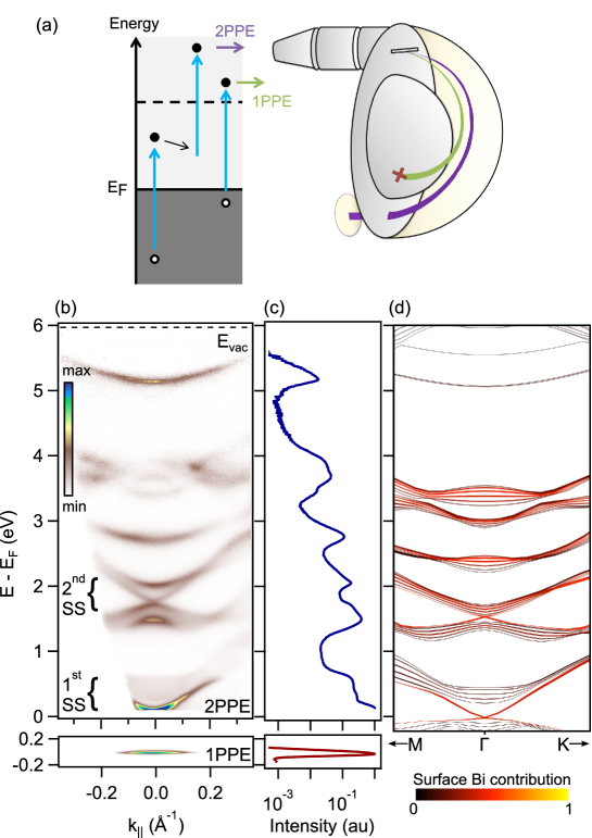
Unless otherwise specified, the measurements in this work were performed with 5.98 eV photons via 1PPE or 2PPE processes. In a 1PPE process, which is the basis for conventional ARPES measurements, a single photon promotes an electron from below the Fermi level to above the vacuum level . It is thereby emitted from the sample surface and collected by a photoelectron analyzer Hüfner (1995). In 2PPE a photon first promotes an electron from below to an unoccupied intermediate state, and a second photon subsequently excites the electron above Haight (1995); Pet (1997); Weinelt (2002); Ohtsubo et al. (2012). Due to the finite time duration of the laser pulses (of order 100 fs in our case), electron relaxation processes can occur in the intermediate states before the electron is photoemitted. These processes are illustrated in Fig. 1(a). Conceptually, the primary distinction is that 1PPE can measure only occupied states, while 2PPE grants access to unoccupied states. Our experimental configuration is identical for both measurements, except for the incident photon intensity. Since 1PPE scales linearly with peak intensity and 2PPE scales quadratically, we switch between 1PPE and 2PPE acquisition modes merely by tuning the intensity. We stress that this is a significant distinction between our measurement and standard 2PPE measurements: Conventional 2PPE is performed with the photon energies chosen to be less than the sample work function, so that an overwhelmingly intense 1PPE signal is avoided. Here we deliberately use photon energies larger than the work function, allowing us to perform both 1PPE and 2PPE. To avoid the intense 1PPE signal while measuring in 2PPE mode, we operate the analyzer such that only electrons with energy are collected, as illustrated in the cartoon of Fig. 1(a).

We begin by presenting the 2PPE and 1PPE spectra of -type Bi2Se3 in the upper and lower panels, respectively, of Fig. 1(b). The 1PPE spectrum consists of only a narrow band of intensity from the occupied portion of the VB above the low-energy cutoff. The reason for this narrow band is that the work function of 5.97 eV is barely exceeded by the photon energy of 5.98 eV. Due to the -type doping, the SS and CB are above , and are absent in the 1PPE spectrum Sobota et al. (2012).
To identify the more novel spectral features, we now turn to the 2PPE spectrum, which reveals states all the way from up to . Here we observe the familiar CB and Dirac SS between and 0.7 eV. These states have the usual characteristics observed in conventional ARPES measurements of -type materials: There is a bandgap of 0.2 eV which is crossed by the linearly dispersive SS Chen et al. (2009); Xia et al. (2009); Chen et al. (2010). We now focus our attention on states which lie at higher energy. We note that the spectral intensity spans a dynamic range of 3 orders of magnitude (see Fig.1(c)) and so the intensities of Fig. 1(b) are rescaled exponentially with energy to allow all features to be displayed simultaneously.
A multitude of features are present in the 2PPE spectrum. In principle, the 2PPE spectral intensity can be complicated by contributions from initial and final states, in addition to the intermediate states which we wish to study Pet (1997); Weinelt (2002). To help clarify the origin of the observed features, we display the calculated band structure in Fig. 1(d). While the energy scales are not reproduced exactly, there is an unambiguous one-to-one correspondence between the observed features and those appearing in the calculation. This gives us confidence that the 2PPE spectrum is representative of the intermediate states.
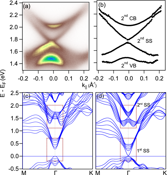
The most intriguing spectral features exist between 1.3 and 2.4 eV, and are shown in detail in Fig. 2(a). Four dispersive bands are observed in this window; for greater clarity, the peak positions obtained by energy distribution curve (EDC) fitting are shown in panel (b). The band structure is strikingly similar to the VB, CB, and SS bands near . In fact, Niesner et. al. identified the linearly dispersive band as an unoccupied topologically protected, spin chiral SS, while the upper and lower bands are the corresponding bulk bandsNiesner et al. (2012). To distinguish these two sets of bands, we refer to the Dirac cone near as the SS, and the higher energy Dirac cone as the SS. The corresponding bulk bands are referred to as the and VB and CB. We note that the experimental resolution in the previous work did not allow for an unambiguous identification of the SS in the gap between the bulk states. Here the spectral separation between the four bands is clearly resolved, allowing us to study the band structure in greater detail. In particular, we resolve the two bulk bands separated by a gap of 530 meV, which is crossed by the linearly dispersive SS. Note, however, that this estimate for the band gap must be regarded as an upper bound for the true value, since it is not known whether the observed electrons are probed from Hüfner (1995). The SS disperses with a velocity of m/s at the Dirac point, which is comparable to the velocity of m/s typically measured for the Fermi velocity of the SS Kuroda et al. (2010). Our calculations confirm the assignment of these bands to bulk and surface states (Fig. 1(d)). Moreover, just like the SS, the SS exists only in the presence of crystal spin-orbit coupling, as evidenced by the calculations in Fig. 2(c) and (d). This suggests that both SSs share the same physical origin, as they both arise due to symmetry inversion of bulk states in the presence of strong spin-orbit coupling.
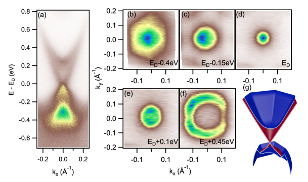
To better characterize the SS, we performed a band mapping to determine its 2-dimensional dispersion. Since band mapping entails rotation of the sample relative to the analyzer, it benefits greatly from having a flat and homogeneous sample. For this we used Bi2Se3 thin films grown by molecular beam epitaxy. These films have -type doping, but we have confirmed that the band structure, including the and SSs, is equivalent to that of the -type crystals. Most importantly, they are extremely flat due to the sapphire substrate upon which they were grown Lee et al. (2012).
The results of the band mapping are summarized in the constant energy maps of Fig. 3. All energies are referenced to the Dirac point of the SS, as shown in panel (a). These results demonstrate that the band structure evolves from a hexagonal bulk band (b), to a circular SS (c-e), to a hexagonal bulk band (f). This is illustrated schematically in Fig. 3(g). This is reminiscent of the SS, which is known to have a circular geometry and be situated between the hexagonal VB and CB Chen et al. (2010); Kuroda et al. (2010). The similarity of their band geometries provides further evidence that the and SSs have similar physical origins.


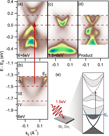
We now discuss the relevance of the SS to studies and applications utilizing ultrafast optical excitation. These applications typically use a photon energy of 1.5 eV due to the use of a Ti:Sapphire laser source, so we investigate the use of 1.5 eV photons to couple to the SS. In Fig. 4(a) we again show the unoccupied SS obtained by 6 eV 2PPE, and in (b) we show the occupied bandstructure of the -type sample obtained by 6 eV 1PPE. Coincidentally, we see that the Dirac point is located almost precisely 1.5 eV above the CB edge, which suggests the possibility of direct ultrafast optical excitation of the SS by driving a transition from the CB. We demonstrate the feasibility of this approach in Fig. 4(c), which is a 2PPE spectrum in which 1.5 eV photons are used to transiently populate the unoccupied states, and 6 eV photons to photoemit. No electrons are excited to states above = 0.17 eV since the corresponding initial states lie above (region I in panel (b)). However, as we expected, the 1.5 eV excitation causes the SS to get populated with electrons from between and the CB edge (region II). The states between -0.24 and 0 eV get only weakly populated, reflecting the fact that few initial states are available due to the bulk bandgap (region III). However, a weak population is observed due to electrons being excited from the SS. The population below -0.24 eV is attributable to a transition from the VB (region IV ) to the VB.
The spectrum of Fig. 4(c) can be understood intuitively as the projection of the initial states below to the unoccupied intermediate states. Fig. 4(a) and (b) can be taken as approximations to the intermediate and initial state band structures, respectively, and we multiply these two spectra as a way of approximating the projection. The result, shown in Fig. 4(d), indeed bears a strong resemblance to the actual 2PPE spectrum in (c). The product spectrum correctly shows the population of the SS attributable to the CB in region II, as well as the population in region IV due to the transition between the two VBs. The only shortcoming is that it overstates the population coming from the SS in region III. However, since this discussion has neglected matrix elements and final state effects, it provides only a qualitative picture. A cartoon illustration of 1.5 eV photoexcitation of Bi2Se3 is provided in Fig. 4(e).
In summary, we have characterized the electronic structure of Bi2Se3 with a combination of 1PPE and 2PPE techniques. 1PPE with 6 eV photons probes the electronic structure below , as is typical for conventional ARPES measurements, while 2PPE with 6 eV photons illuminates the states between and . This technique reveals a Dirac SS located 1.5 eV above the CB edge, and we have further shown that excitation with 1.5 eV photons drives a direct transition between these two states.
There are a number of interesting implications of these results. First, to our knowledge, this is the first measurement on any material using a single photon energy for both 1PPE and 2PPE. This is achieved by using a photon energy exceeding the sample work function, which has conventionally been avoided in 2PPE measurements. Since the only experimental parameter tuned between 1PPE and 2PPE modes of operation is the intensity, this represents an exceptionally simple method to determine both the occupied and unoccupied band structure of a material. This has exciting implications, for example, for materials such as the high- cuprates, where a measurement of both the occupied and unoccupied sides of the energy gap would provide insight on the particle-hole asymmetry of the superconducting and pseudogap states Hashimoto et al. (2010); Moritz et al. (2011).
Next, we emphasize how this work builds on that of Niesner et. al. by using superior spectral resolution to provide unambiguous evidence of the SS Niesner et al. (2012). This state is expected to have all the novel topological and spin properties which characterize the well-known Dirac SS of TIs Niesner et al. (2012); Eremeev et al. (2013). Our demonstration that it is populated by 1.5 eV photons could have relevance for the number of existing studies on -type TIs which have utilized 1.5 eV photons Qi et al. (2010); Kumar et al. (2011); Hsieh et al. (2011); Wang et al. (2012b); Hajlaoui et al. (2012); Crepaldi et al. (2012); McIver et al. (2012). These experiments have been interpreted without knowledge of the unoccupied topological SS, and it would be interesting to evaluate whether the transition into this state plays a role in the physics discussed in those results. Finally, the fact that it can be accessed by 1.5 eV photons is particularly appropriate for applications, since this is the fundamental photon energy provided by commercial ultrafast Ti:Sapphire lasers. This discovery therefore demonstrates a unique opportunity for direct ultrafast optical coupling to TI SSs.
Acknowledgements.
This work is supported by the Department of Energy, Office of Basic Energy Sciences, Division of Materials Science. JAS acknowledges support by the Stanford Graduate Fellowship. AFK is supported by the Laboratory Directed Research and Development Program of Lawrence Berkeley National Laboratory under the U.S. Department of Energy contract number DE-AC02-05CH11231.References
- Fu et al. (2007) L. Fu, C. Kane, and E. Mele, Phys. Rev. Lett. 98, 106803 (2007).
- Zhang et al. (2009) H. Zhang et al., Nature Phys. 5, 438 (2009).
- Chen et al. (2009) Y. L. Chen et al., Science 325, 178 (2009).
- Xia et al. (2009) Y. Xia et al., Nature Phys. 5, 398 (2009).
- Hsieh et al. (2009a) D. Hsieh et al., Science 323, 919 (2009a).
- Hsieh et al. (2009b) D. Hsieh et al., Nature 460, 1101 (2009b).
- Roushan et al. (2009) P. Roushan et al., Nature 460, 1106 (2009).
- Garate and Franz (2010) I. Garate and M. Franz, Phys. Rev. Lett. 104, 146802 (2010).
- Aguilar et al. (2011) R. V. Aguilar et al., (2011), arXiv:1105.0237 .
- Wang et al. (2012a) J. Wang, H. Mabuchi, and X.-L. Qi, (2012a), arXiv:1209.6597 .
- Hosur (2011) P. Hosur, Phys. Rev. B 83, 035309 (2011).
- McIver et al. (2012) J. W. McIver et al., Nature Nanotech. 7, 96 (2012).
- Sobota et al. (2012) J. A. Sobota et al., Phys. Rev. Lett. 108, 117403 (2012).
- Qi et al. (2010) J. Qi et al., Appl. Phys. Lett. 97, 182102 (2010).
- Kumar et al. (2011) N. Kumar et al., Phys. Rev. B 83, 235306 (2011).
- Hsieh et al. (2011) D. Hsieh et al., Phys. Rev. Lett. 107, 077401 (2011).
- Wang et al. (2012b) Y. H. Wang et al., Phys. Rev. Lett. 109, 127401 (2012b).
- Hajlaoui et al. (2012) M. Hajlaoui et al., Nano Lett. 12, 3532 (2012).
- Crepaldi et al. (2012) A. Crepaldi et al., Phys. Rev. B 86, 205133 (2012).
- Ueda et al. (1999) Y. Ueda et al., J. Electron. Spectrosc. Relat. Phenom. 101-103, 677 (1999).
- Niesner et al. (2012) D. Niesner et al., Phys. Rev. B 86, 205403 (2012).
- Eremeev et al. (2013) S. V. Eremeev et al., JETP Lett. 96, 780 (2013).
- Lee et al. (2012) J. J. Lee et al., Appl. Phys. Lett. 101, 013118 (2012).
- Perdew et al. (1996) J. P. Perdew, K. Burke, and M. Ernzerhof, Phys. Rev. Lett. 77, 3865 (1996).
- Blaha et al. (2001) P. Blaha et al., wien2k: An Augmented Plane Wave Plus Local Orbitals Program for Calculating Crystal Properties, edited by K. Schwarz (Techn. Universitat Wein, Austria, 2001).
- Nakajima (1963) S. Nakajima, J. Phys. Chem. Solids 24, 479 (1963).
- Hüfner (1995) S. Hüfner, Photoelectron Spectroscopy (Springer, Berlin, 1995).
- Haight (1995) R. Haight, Surf. Sci. Rep. 21, 275 (1995).
- Pet (1997) Prog. in Surf. Sci. 56, 239 (1997).
- Weinelt (2002) M. Weinelt, J. Phys.: Condens. Matter 14, R1099 (2002).
- Ohtsubo et al. (2012) Y. Ohtsubo et al., Phys. Rev. Lett. 109, 226404 (2012).
- Chen et al. (2010) Y. L. Chen et al., Science 329, 659 (2010).
- Kuroda et al. (2010) K. Kuroda et al., Phys. Rev. Lett. 105, 076802 (2010).
- Hashimoto et al. (2010) M. Hashimoto et al., Nature Phys. 6, 414 (2010).
- Moritz et al. (2011) B. Moritz et al., Phys. Rev. B 84, 235114 (2011).