Electronic Structure of the Metallic Antiferromagnet PdCrO2 Measured by Angle-Resolved Photoemission Spectroscopy
Abstract
PdCrO2 is material which has attracted interest due to the coexistence of metallic conductivity associated with itinerant Pd electrons and antiferromagnetic order arising from localized Cr spins. A central issue is determining to what extent the magnetic order couples to the conduction electrons. Here we perform angle-resolved photoemission spectroscopy (ARPES) to experimentally characterize the electronic structure. We find that the Fermi surface has contributions from both bulk and surface states, which can be experimentally distinguished and theoretically verified by slab band structure calculations. The bulk Fermi surface shows no signature of electronic reconstruction in the antiferromagnetic state. This observation suggests that there is negligible interaction between the localized Cr spin structure and the itinerant Pd electrons measured by ARPES.
I Introduction
Many strongly correlated electronic phases of matter exist in close proximity to antiferromagnetic (AFM) order, such as the high-temperature superconductivity of cuprates Lee and Wen (2006) and iron pnictides, Zhao et al. (2008) as well as the heavy fermion behavior of -electron systems.Si and Steglich (2010) In heavy fermion materials, for example, mobile conduction electrons form a bound resonance with localized magnetic moments, causing the electron effective mass to increase by a factor of 1000 as compared to conventional metals. A complete understanding of these materials has proven elusive due to the competition or coexistence of several phases, such as paramagnetism, antiferromagnetism, and unconventional superconductivity.Lee and Wen (2006); Zhao et al. (2008); Si and Steglich (2010) It is therefore of interest to study the interaction of mobile conduction electrons and localized magnetic moments in a less complicated system where the physics may be more easily understood.
PdCrO2 is material which has attracted attention due to the rich physics of its geometrically frustrated spin system.Takatsu et al. (2009a, b, 2010a, 2010b) The material crystallizes in a delafossite structure with symmetry, and can be described as alternating stacked layers of Pd and Cr triangular lattices. The localized spins of the Cr3+ ions () exhibit AFM order at K by forming a 120∘ spin structure with periodicity.Mekata et al. (1995) The material also exhibits metallic conductivity due to the Pd electrons.Takatsu et al. (2009b) The physical properties of PdCrO2 are analogous to those of the isostructural compound PdCoO2, which also has metallic conductivity due to its Pd electrons.Tanaka et al. (1998); Hicks et al. (2012) The replacement of Co with Cr, however, introduces localized spins, and thus provides a system in which to study the coexistence of magnetic order and metallic conduction.Takatsu et al. (2009a); Ong and Singh (2012) Moreover, frustration effects arising from the geometric arrangement of the spins have unique signatures in transport measurements, lead to unusual critical exponent behavior,Takatsu et al. (2009b) and also play a role in the recent observation of the unconventional anomalous Hall effect. Takatsu et al. (2010b)
Here we report an angle-resolved photoemission spectroscopy (ARPES) and band structure calculation study of the electronic structure of PdCrO2 both above and below . The bulk Fermi surface (FS) is found to consist of a single hexagonal electron pocket. In addition, surface states corresponding to a Pd-terminated crystal are identified. We detect no signatures of electronic reconstruction in the AFM state. This experimental observation suggests that the AFM order plays a negligible role in shaping the electronic structure of the itinerant Pd electrons measured by ARPES.
II Methods
High-quality single crystals of PdCrO2 were grown by a flux method and characterized with powder x-ray diffraction and energy dispersive x-ray analysis.Takatsu and Maeno (2010) The ARPES measurements were performed at beamline 10.0.1 of the Advanced Light Source using linearly polarized photons of energy 55 eV. A Scienta R4000 hemispherical analyzer was used, with a total energy resolution of 20 meV and an angle resolution of 0.25∘, corresponding to a momentum resolution of 0.005 Å-1. The samples were cleaved at a base pressure torr.
For bulk band structure calculations, we have used the full potential linearized augmented plane wave (FLAPW) method with local orbital (FLAPW+LO, APW+lo+LO), implemented in Wien2kBlaha et al. (2001) in the generalized gradient approximation (GGA). Since our ARPES data includes contributions from surface states, we have additionally performed slab band structure calculations. These calculations simulate the broken translational symmetry at the sample surface by employing a superstructure of stacked layers separated by a vacuum region. For our calculations, we considered hexagonal unit cells separated by about 20 Å of vacuum along the -axis. Each hexagonal unit cell contains 6 Cr layers, which was found to be sufficient to screen the surface effect and reasonably reproduce the bulk band structure. The vacuum dimension is large enough so that there is effectively no hybridization between surface atoms through the vacuum.
III Results
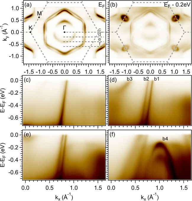
In Figs. 1(a) and (b), we show constant-energy maps of the ARPES intensity at the Fermi energy and at eV, respectively, at a measurement temperature of 10 K. There are three electron-like FS pockets, all centered at the -point, with dispersions as shown in the energy-momentum cuts of Figs.1(c)-(f). Bands b1 and b2 have hexagonal FSs and disperse linearly, while b3 disperses parabolically and has an essentially circular FS (Fig. 1(a)). The intensity of b2 and b3 are suppressed around due to photoemission matrix elements.Damascelli and Shen (2003) In addition to these three bands which cross , there exist hole bands b4 centered at the M-point at eV binding energy. The ARPES intensity is periodic with respect to the Brillouin zone (BZ) boundaries (indicated by grey dashed lines in Figs. 1(a) and (b)), which is consistent with the lattice’s hexagonal symmetry. From the periodicity we estimate a lattice constant of 2.970.06 Å, which is consistent with the known value of the bulk lattice constant of 2.93 Å.Takatsu et al. (2009b)
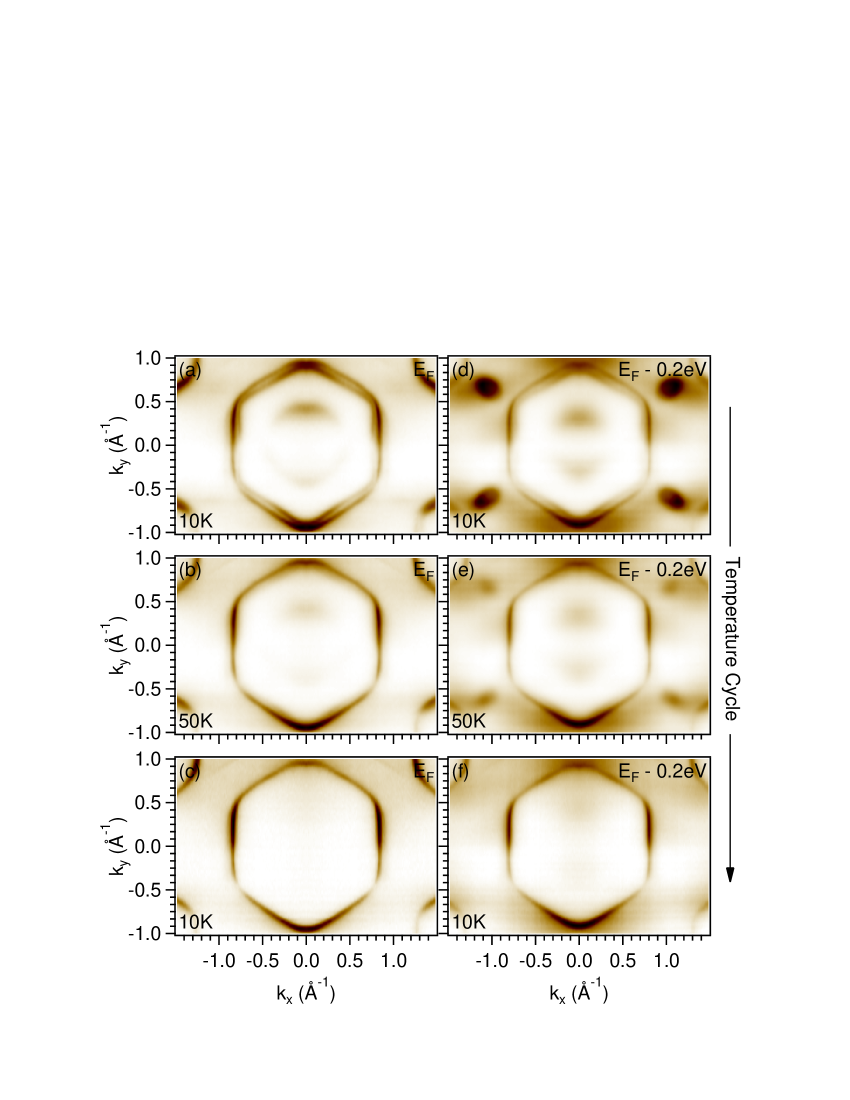
We now show that these bands can be experimentally determined to consist of bulk and surface states. This insight is gained by cycling the sample temperature. Specifically, we raised the sample temperature from 10 K to 50 K, and subsequently lowered the temperature back to 10 K. During the warming process the chamber pressure temporarily increased up to torr due to outgassing from the sample manipulator. Constant-energy maps at the elevated and lowered temperatures are displayed in Fig. 2. The most striking observation is the disappearance of intensity from bands b2, b3, and b4 during the warming process, which does not recover after cooling the sample back to low temperature. This irreversibility suggests that the change is due to sample surface contamination from the degassing process. The disappearance of bands b2, b3, and b4 indicates that they originate from surface states, while the surviving pocket b1 is a bulk state. (We note that the same thermal-cycling procedure has been successfully applied to distinguish surface and bulk states in PdCoO2Noh et al. (2009) and related compounds.Yang et al. (2005)) The b1 pocket has an area of 456% of the BZ, and can therefore be attributed to one Pd 4 conduction electron per unit cell.
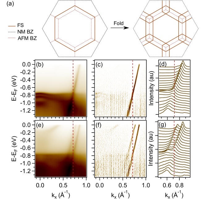
We note that the geometry of the bulk FS b1 is unchanged between 10 K and 50 K (Figs. 2(b) and (c)), which are temperatures below and above respectively. This comparison suggests that the AFM order plays a negligible role in shaping the electronic structure. This is surprising because the AFM spin structure reduces the non-magnetic (NM) BZ to an AFM BZ with the area, and coupling to this reduced periodicity should lead to a corresponding reconstruction of the band structure,Voit (2000) as illustrated in Fig. 3(a). Although no such folding is immediately observed, it is prudent to inspect the data carefully since the so-called shadow bands could have weaker spectral weight than the non-reconstructed bands. Voit (2000); Brouet et al. (2004)
In Fig. 3(b) we show a cut through , equivalent to Fig. 1(c) but plotted over a larger energy scale, at a measurement temperature 10 K . In the presence of AFM reconstruction the band b1 would fold across the AFM BZ boundary, represented by the red dashed line. In Fig. 3(c) we plot the 2 derivative along , which serves to remove slowly varying background features such as the intense valence states at 750 meV binding energy, and is therefore highly sensitive to weak spectral features. Even after this procedure there is no indication of band folding across the AFM BZ boundary. A close inspection of the momentum distribution curves (Fig. 3(d)) is consistent with the absence of band folding. The same analysis is shown in Figs. 3(e)-(g) for Å, corresponding to the cut in Fig. 1(d). This cut contains b2 in addition to b1, but again no reconstruction of either band is observed. We therefore conclude that the ARPES data contains no signatures of reconstruction in the AFM state of PdCrO2.
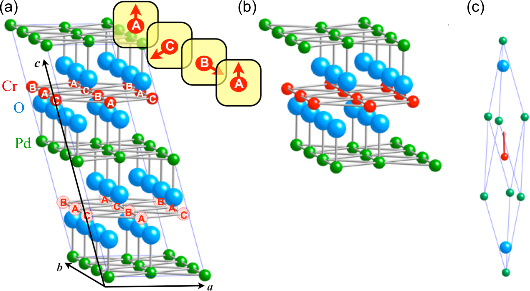
To better understand the electronic structure we have performed a number of band structure calculations. We begin by computing the bulk band structure with AFM spin configuration, which reflects the magnetic ordering of the material below . Since the interlayer magnetic coupling is not known, we considered both antiparallel and parallel coupling between the Cr layers, as illustrated in Figs. 4(a) and (b). We find that both configurations are degenerate, suggesting a weak Cr-Cr interlayer coupling. The calculated FS for parallel interlayer coupling is shown in Fig. 5(a), and can be understood as originating from a single hexagonal pocket in the NM BZ which is then folded into the AFM BZ. This understanding is consistent with the cartoon picture of Fig. 3(a). However, when comparing to the experimental data, this result has two discrepancies: (1) As discussed above, the experimental data shows no indication of band folding due to the AFM order, and (2) The experimental data includes contributions from surface states, which are absent in these calculation results.
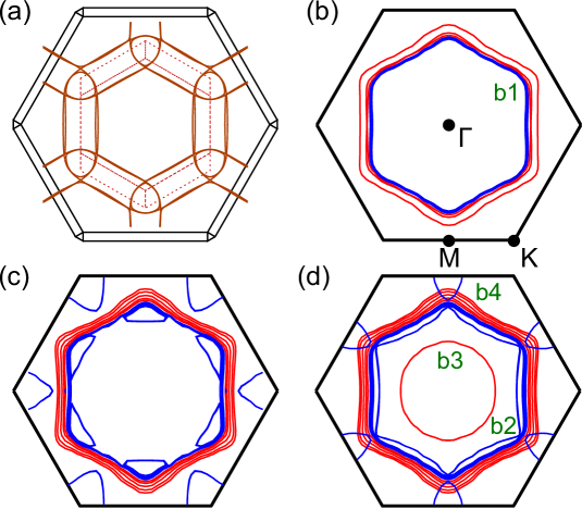
The first discrepancy is a fundamental consequence of the periodicity of the AFM configuration used in the calculation. To obtain a calculation result which resembles the experimental data, we must instead choose a configuration in which the periodicity is equivalent to that of the NM unit cell. The simplest model with this periodicity, which also maintains the same local (polarized) spin structure as the AFM state, is a ferromagnetic (FM) spin configuration, illustrated in Fig. 4(c). The calculated FS for this configuration is shown in Fig. 5(b). As expected, the equivalence of the FM and NM unit cells implies that the electronic structure undergoes no reconstruction. In fact, the resulting hexagonal pocket agrees well with b1 observed in ARPES, except for a small spin-splitting arising from the FM order (red and blue colors in Fig. 5(b)).
The second discrepancy, the absence of surface states, can be overcome by performing a slab band structure calculation. This type of calculation simulates a sample surface by employing a superstructure of stacked layers separated by a vacuum region. We continue to consider FM order to avoid reconstruction effects as discussed above. Both Pd- and O- terminated surface conditions have been considered. The calculation results are shown in Figs. 5(c) and (d). In both cases, a number of FS pockets in addition to the bulk hexagon are observed, and can be identified as surface states. In the O-terminated case, there are small FS pockets in the corners of the hexagon of b1, as well as pockets centered at K, neither of which were observed in the experiment. In the Pd-terminated case, a small inner-hexagon and circular electron pockets are observed, which can be identified with bands b2 and b3 observed in ARPES. The calculation reveals an additional hole pocket centered at the M-point, which is not observed experimentally. However, this pocket resembles the M-point hole bands observed at higher binding energy (see Fig. 1(b)), so we identify this state with b4. It is not clear why the binding energy of this band in the calculation disagrees so severely with experiment, but it may be associated with the fact that the FM spin configuration used in these calculations does not represent the true AFM order of the sample.
IV Discussion
Using ARPES we have experimentally characterized the electronic structure of PdCrO2. The bulk FS is found to consist of a single hexagonal electron pocket which is attributed to one Pd 4 conduction electron per unit cell. This electronic structure bears a strong resemblance to that of PdCoO2, which also consists of a single hexagonal electron pocket from its Pd 4 electrons.Noh et al. (2009) In addition, we observe electron pockets attributed to surface states. From the slab band structure calculations we can identify that these states originate from a Pd-terminated surface. This contrasts the situation of PdCoO2, in which ARPES reveals features associated with a O-terminated surface, but not a Pd- terminated surface.Noh et al. (2009); Kim et al. (2009) It is not understood why these two similar crystal structures should favor different surface terminations.
The deeper issue is the discrepancy between the non-reconstructed bands measured in ARPES and the reconstructed band structure expected for AFM order.Ong and Singh (2012) There are a number of examples of ARPES resolving band structure reconstruction in systems modulated by periodic potentials. In the CeTe3 system, for example, upon entering the charge density wave state the FS becomes gapped where it intersects the ordering vector, with a concomitant formation of folded shadow bands. Brouet et al. (2004) Similar observations of gapping and folded shadow bands have been made in the spin density wave state of (Ba,Sr)Fe2As2. Yi et al. (2009) Here we believe it is important to note a significant distinction between the density waves in these examples and the AFM state of PdCrO2. In these examples, the electrons associated with the reconstructed bands directly participate in the ordering. For example, the gapped electrons in CeTe3 are precisely those whose densities are modulated by the charge density wave. In fact, the band reconstruction is thought to be a driving force for the density waves by providing a mechanism by which to lower the electronic kinetic energy.Schmitt et al. (2011) Similarly, in the (Ba,Sr)Fe2As2 system it is believed that the itinerant electrons directly participate in the magnetic order.Hu et al. (2008) The situation is quite different in PdCrO2, where the Pd conduction electrons themselves are not responsible for the order, but merely coexist with the AFM order coming from the Cr moments.Takatsu et al. (2009a) It is therefore not clear to what extent the conduction electrons should experience the periodic potential of the magnetic moments. Since the spectral weight of the folded shadow bands is expected to be proportional to this coupling potential, Brouet et al. (2004); Voit (2000) the absence of shadow bands may be taken as experimental evidence for weak coupling between the Pd 4 conduction electrons and the localized Cr spins. A similar example is found in EuFe2As2, where Eu contributes localized, ordered magnetic moments, and Fe2As2 contributes itinerant conduction electrons. In this material, it is found that the low-energy electronic structure is nearly decoupled from the localized magnetic order. Jeevan et al. (2008)
Finally, we wish to acknowledge recent observations of de Haas-van Alphen (dHvA) oscillations in PdCrO2, which suggest the presence of several small FS pockets consistent with FS reconstruction in the AFM state. Ok et al. (2013) This seeming contradiction between ARPES and dHvA results is strongly reminiscent of the case for underdoped cuprates, where ARPES reports a large FS or open arcs, Damascelli and Shen (2003) but dHvA oscillations report small, closed FS pockets. Doiron-Leyraud et al. (2007) This discrepancy is not understood and is the subject of intense debate. In our case, one possible interpretation is based on the surface-sensitivity of ARPES as compared to the bulk-sensitivity of dHvA experiments. From the universal curve for inelastic mean free path of electrons in solids, we estimate that the 55 eV photons probe a sample depth of 0.5 nm. Seah and Dench (1979) This is substantially less than the -axis lattice parameter of 1.8 nm and implies that our technique is highly surface sensitive.Takatsu et al. (2009b) While the bulk of the sample is known to have AFM order from transport and neutron scattering experiments, Takatsu et al. (2009b) it is not known whether this order necessarily persists up to the surface. The absence of shadow bands could therefore be attributed to short-range or non-existent AFM order near the surface of the sample. On the other hand, another possible explanation is that the high magnetic fields used in dHvA experiments perturb the ground state of the material and lead to reconstructions which do not exist in the zero-field state probed by ARPES. Similar explanations have been proposed for the cuprate experiments. Chen et al. (2008) Further studies of dHvA oscillations, neutron scattering, and low photon energy ARPES (to achieve deeper bulk sensitivity) may be instrumental in resolving this issue.
V Conclusions
We performed angle-resolved photoemission spectroscopy experiments on single-crystal samples of the compound PdCrO2, which consists of alternating stacked layers of Pd and Cr triangular lattices. We observed a large hexagonal bulk Fermi surface centered at the -point, attributed to the Pd conduction electrons, as well as three surface-derived bands associated with a Pd-terminated crystal surface. There was no electronic reconstruction observed with respect to the magnetic ordering of the Cr spins at = 37.5 K. This result suggests that the Pd conduction electrons are weakly coupled to the magnetic order of the Cr spins. Further investigations such as de Haas-van Alphen oscillation measurements and neutron scattering experiments are important for further clarifying the interplay between the Pd conduction electrons and the Cr localized spins.
Acknowledgements.
We acknowledge P. S. Kirchmann, R. G. Moore, I. M. Vishik, and S. Yang for fruitful discussions and experimental assistance. The work at SLAC, Stanford, and LBNL is supported by the Department of Energy, Office of Basic Energy Sciences, Division of Materials Science. JAS acknowledges support by the Stanford Graduate Fellowship. KK and BIM acknowledge support by the NRF (Grants No. 2009-0079947 and No. 2011-0025237). HT and YM acknowledge support by MEXT KAKENHI (Grant No. 21340100), HT also by MEXT KAKENHI (Grant No. 24740240).References
- Lee and Wen (2006) P. A. Lee and X.-G. Wen, Rev. Mod. Phys. 78, 17 (2006).
- Zhao et al. (2008) J. Zhao, Q. Huang, C. de la Cruz, S. Li, J. W. Lynn, Y. Chen, M. A. Green, G. F. Chen, G. Li, Z. Li, J. L. Luo, N. L. Wang, and P. Dai, Nature Mater. 7, 953 (2008).
- Si and Steglich (2010) Q. Si and F. Steglich, Science 329, 1161 (2010).
- Takatsu et al. (2009a) H. Takatsu, H. Yoshizawa, and Y. Maeno, J. Phys.: Conf. Ser. 145, 12046 (2009a).
- Takatsu et al. (2009b) H. Takatsu, H. Yoshizawa, S. Yonezawa, and Y. Maeno, Phys. Rev. B 79, 104424 (2009b).
- Takatsu et al. (2010a) H. Takatsu, S. Yonezawa, C. Michioka, K. Yoshimura, and Y. Maeno, J. Phys.: Conf. Ser. 200, 012198 (2010a).
- Takatsu et al. (2010b) H. Takatsu, S. Yonezawa, S. Fujimoto, and Y. Maeno, Phys. Rev. Lett. 105, 137201 (2010b).
- Mekata et al. (1995) M. Mekata, T. Sugino, A. Oohara, Y. Oohara, and H. Yoshizawa, Physica B 213-214, 221 (1995).
- Tanaka et al. (1998) M. Tanaka, M. Hasegawa, T. Higuchi, T. Tsukamoto, Y. Tezuka, S. Shin, and H. Takei, Physica B 245, 157 (1998).
- Hicks et al. (2012) C. W. Hicks, A. S. Gibbs, A. P. Mackenzie, H. Takatsu, Y. Maeno, and E. A. Yelland, Phys. Rev. Lett. 109, 116401 (2012).
- Ong and Singh (2012) K. P. Ong and D. J. Singh, Phys. Rev. B 85, 134403 (2012).
- Takatsu and Maeno (2010) H. Takatsu and Y. Maeno, J. Cryst. Growth 312, 3461 (2010).
- Blaha et al. (2001) P. Blaha, K. Schwarz, G. Madsen, D. Kvasnicka, and J. Luitz, WIEN2k, An Augmented Plane Wave Plus Local Orbitals Program for Calculating Crystal Properties, edited by K. Schwarz (Techn. Universitat Wein, Austria, 2001).
- Damascelli and Shen (2003) A. Damascelli and Z.-X. Shen, Rev. Mod. Phys. 75, 473 (2003).
- Noh et al. (2009) H.-J. Noh, J. Jeong, J. Jeong, E.-J. Cho, S. B. Kim, K. Kim, B. I. Min, and H.-D. Kim, Phys. Rev. Lett. 102, 256404 (2009).
- Yang et al. (2005) H.-B. Yang, Z.-H. Pan, A. K. P. Sekharan, T. Sato, S. Souma, T. Takahashi, R. Jin, B. C. Sales, D. Mandrus, A. V. Fedorov, Z. Wang, and H. Ding, Phys. Rev. Lett. 95, 146401 (2005).
- Voit (2000) J. Voit, Science 290, 501 (2000).
- Brouet et al. (2004) V. Brouet, W. L. Yang, X. J. Zhou, Z. Hussain, N. Ru, K. Y. Shin, I. R. Fisher, and Z. X. Shen, Phys. Rev. Lett. 93, 126405 (2004).
- Kim et al. (2009) K. Kim, H. C. Choi, and B. I. Min, Phys. Rev. B 80, 035116 (2009).
- Yi et al. (2009) M. Yi, D. H. Lu, J. G. Analytis, J.-H. Chu, S.-K. Mo, R.-H. He, M. Hashimoto, R. G. Moore, I. I. Mazin, D. J. Singh, Z. Hussain, I. R. Fisher, and Z.-X. Shen, Phys. Rev. B 80, 174510 (2009).
- Schmitt et al. (2011) F. Schmitt, P. S. Kirchmann, U. Bovensiepen, R. G. Moore, J.-H. Chu, D. H. Lu, L. Rettig, M. Wolf, I. R. Fisher, and Z.-X. Shen, New J. Phys. 13, 063022 (2011).
- Hu et al. (2008) W. Z. Hu, J. Dong, G. Li, Z. Li, P. Zheng, G. F. Chen, J. L. Luo, and N. L. Wang, Phys. Rev. Lett. 101, 257005 (2008).
- Jeevan et al. (2008) H. S. Jeevan, Z. Hossain, D. Kasinathan, H. Rosner, C. Geibel, and P. Gegenwart, Phys. Rev. B 78, 052502 (2008).
- Ok et al. (2013) J. M. Ok, Y. J. Jo, K. Kim, T. Shishidou, E. S. Choi, H.-J. Noh, T. Oguchi, B. I. Min, and J. S. Kim, (2013), arXiv:1302.3962 .
- Doiron-Leyraud et al. (2007) N. Doiron-Leyraud, C. Proust, D. LeBoeuf, J. Levallois, J.-B. Bonnemaison, R. Liang, D. A. Bonn, W. N. Hardy, and L. Taillefer, Nature 447, 565 (2007).
- Seah and Dench (1979) M. P. Seah and W. A. Dench, Surf. Interface Anal. 1, 2 (1979).
- Chen et al. (2008) W.-Q. Chen, K.-Y. Yang, T. M. Rice, and F. C. Zhang, EPL 82, 17004 (2008).