e-mail: pavlyk@electronics.wups.lviv.ua††thanks: 107, Tarnawsky Str., Lviv 79017, Ukraine ††thanks: 107, Tarnawsky Str., Lviv 79017, Ukraine††thanks: 107, Tarnawsky Str., Lviv 79017, Ukraine\sanitize@url\@AF@joine-mail: pavlyk@electronics.wups.lviv.ua††thanks: 107, Tarnawsky Str., Lviv 79017, Ukraine\sanitize@url\@AF@joine-mail: pavlyk@electronics.wups.lviv.ua††thanks: 50, Drahomanov Str., Lviv 79005, Ukraine
ELECTROPHYSICAL CHARACTERISTICS
OF NEAR-SURFACE LAYERS IN
-Si
CRYSTALS
WITH SPUTTERED Al FILMS AND SUBJECTED
TO ELASTIC DEFORMATION
Abstract
The deposition of Al film onto the (111) surface of a p-Si crystal was shown to induce a deformation in the near-surface layer of the latter. Provided that the crystal strain is elastic and uniaxial, the gettering of defects in the near-surface layer is observed, which is confirmed by a change in the dependence of the specimen resistance on the elastic strain magnitude. The maximum depth of the defect capture has been calculated on the basis of the energy of interaction between the deformed layer and dislocations.
1 Introduction
Our understanding of a deformation in silicon is mainly reduced to a change in the equilibrium state of the silicon crystal lattice under the action of external stresses. Owing to a modification of the crystal lattice, the parameters of the electron band structure in silicon also change. Variations in the mobility of charge carriers, their capture cross-section, concentration of defects, and so on result in a variation of defects total electric conductivity, the latter being strongly dependent on the strength, direction, and type of a crystal deformation.
Mechanical stresses in a silicon substrate can also be induced when a metallic or dielectric film is grown on its surface. Mechanical stresses in the plane of contact between the film and the substrate arise owing to a mismatch between the parameters of their lattices [1]. For instance, the mismatch between the crystal lattice parameters for silicon and aluminum is about 25%. Under the action of a biaxial strain, the charge carriers become more mobile (as a rule, by 50 to 70%), which results in a reduction of the resistance in the strained crystal layer [2].
During the formation of a film on the semiconductor surface, there emerge regions of mechanical stresses, where defects of various types can be localized. This region can also stimulate a generation of dislocations, e.g., at the following plastic deformation [3].
This work aims at studying the influence of the deformation fields formed as a result of the metal film sputtering onto the surface of p-silicon crystals subjected to uniaxial and elastic strain on the electro-physical characteristics of those crystals.
2 Experimental Technique
Specimens to study were cut out from a wafer of single-crystalline silicon of the p-type (KDB-10 grade). After the standard procedures of cutting, grinding, and chemical polishing, the both specimen facets (111) were covered with Al film contacts 90 nm in thickness. The Al films were deposited in a vacuum chamber VUP-5M at a pressure of 10-2 Pa and a temperature of 350 in such a way that the surface edges were covered by the film, whereas its central part remained free [4]. With the use of the thermocompression welding technique, gold wires were attached to the Al films. In their turn, the wires were soldered to the input contacts of a measuring unit.
Electroconductivity measurements were carried out on a vacuum deformation installation at room temperature and a residual gas pressure of 10-2 Pa. The external strain was applied cyclically, in the elastic deformation interval, along the crystallographic direction [112] (i.e. in parallel to the lateral facets (111) and (110) of a rectangular specimen) with the pressure forces up to 40 MPa and at deformation rates of 8 and 32 . One cycle of uniaxial strain included the stages of specimen squeezing, deformation relief, and specimen holding between those stages at room temperature for a period varying from a few minutes to an hour.
After the mechanically stimulated changes in the electric conductivity had been measured, the aluminum film was etched. The obtained surface (111) of the specimen was selectively etched, and then its structural researches were carried out with the use of optical, electron, and atomic force microscopies. Afterward, the studied surface was etched again, layer-by-layer at a low etching rate, and examined on an optical microscope.
3 Theoretical Calculations
The crystal lattice of silicon has a diamond cubic structure with the lattice parameter nm and the shortest interatomic distance equal to 0.24 nm. The plane (111) is characterized by the closest packing of atoms, and the corresponding calculated interatomic distance amounts to 0.375 nm. If the near-surface layer of single-crystalline silicon contacts with a material, in which the lattice period differs from that of silicon, there emerges a near-contact region, the layers in which have intermediate values of lattice parameter. As a result, such a mismatch induces mechanical stresses in the single crystal described by a deformation potential. The symmetry of crystal layers decreases at that, and two lattice parameters have to be introduced. Below, the lattice constant in the (111) plane will be denoted as , and that in the direction perpendicular to the plane (111) as .
Aluminum has a face-centered cubic packing, its crystal lattice parameter amounts to 0.408 nm, and the shortest interatomic distance equals 0.289 nm. Our computer simulation showed that atoms in the aluminum lattice also have the closest packing characterized by the minimum interatomic distance, as was for the (111) plane of silicon. Therefore, when aluminum is deposited onto the silicon (111) surface, the aluminum atoms also form the plane (111), because this arrangement is the most beneficial energetically, since the deformations in the contacting crystal lattices are minimal. It should be noted that, according to the results of work [5], the diffusion coefficient of Al atoms is close to zero at the indicated temperatures of their sputtering onto the Si surface; therefore, the diffusion of Al into Si was practically absent.
For silicon, which is a covalent crystal, the binding energy of atoms in the crystal lattice is equal to the sum of the energies of individual atoms, the energies of electrostatic interactions (electron–electron, electron–nucleus, and nucleus–nucleus ones), and the energy of exchange interaction emerging owing to the electron exchange [6, 7]. Hence, the total energy looks like
| (1) |
where is the energy of a single atom, the energy of electrostatic interactions, the energy of exchange interaction, the integral of non-orthogonality (its value falls within the interval from 0 to 1), and the interatomic distance. The corresponding binding energy for atoms in the aluminum crystal lattice equals
| (2) |
where is the Madelung constant, and the electron charge. Hence, the magnitude of silicon atom displacement in the near-surface layer is proportional to the force, with which the aluminum atoms act on it; it is also true for aluminum atoms in the near-surface layer. According to the results of work [8], the distance between Si and Al atoms amounts to 0.254 nm. Therefore, from formulas (1) and (2), we can calculate the corresponding values for the displacements of atoms in the first atomic layers. As a result, we obtain nm and nm.
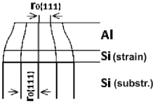
Let the deformed region consist of three layers with different thicknesses. These are (Fig. 1) the aluminum film with a deformed lattice practically across the whole film thickness, a few atomic layers of silicon with a deformed lattice, and the substrate with a non-deformed structure. To make calculations simpler, let us assume that the strain is uniform across the thickness of each layer, ; in other words, the averaged values of atomic displacements from the corresponding equilibrium positions are used. According to elasticity theory [9], the mechanical stress in a uniform crystal film with the “undeformed” lattice constant and thickness is determined by the expression
| (3) |
where and are the Young modulus and Poisson’s ratio, respectively, for the -th layer. The relative deformation in each layer is determined by a tensor, in which ,
| (4) |
and
| (5) |
Here, and are the average thicknesses, and the average lattice parameters, and the Young moduli, and and Poisson’s ratios for the deformed substrate layer and the sputtered film, respectively.
The total energy of the heterostructure equals
| (6) |
It consists of three components: the energy of mismatch deformations, the energy of interaction between mismatch deformations and misfit dislocations, and the energy of misfit dislocations. Provided that the initial conditions for the formation of the epitaxial layer were so set that misfit dislocations are not formed (in particular, a substrate temperature of 350 and the absence of external stresses), the total energy is determined by the expression
| (7) |
where is the sputtered film area, and is the coordinate reckoned into the crystal depth.
The energy of edge dislocations located in the crystal bulk before the epitaxial sputtering is calculated by the formula
| (8) |
where is the concentration of dislocation outcrops on the surface of silicon crystal, the shear modulus, the absolute value of Burgers vector, the average dislocation length, and the dislocation core radius. If an external mechanical loading is applied to the crystal, the energy of the near-surface contact layer changes by the magnitude
| (9) |
where is the force applied to the crystal, the initial crystal length, and the area of the crystal substrate, to which the force is applied. The sign plus is selected if the external strain and the mechanical field under the film simultaneously squeeze or stretch the crystal lattice. But if the external loading acts oppositely to the near-surface strain field, the sign minus should be selected.
The edge dislocation, in its turn, can bend and move in the direction perpendicular to that external strain. The concentration of dislocation outcrops on the surface (, in units) also varies at that, and, consequently, the energy of dislocations in the near-surface region changes proportionally to .
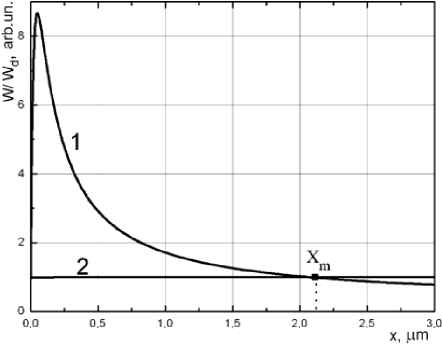
The plot describing the dependence of the ratio between the energy of the deformed layer and the energy of a dislocation in the course of external mechanical loading on the coordinate is depicted in Fig. 2. One can see that the corresponding curves intersect at the point , the maximum depth of defect capture by the near-surface layer from edge dislocations. Its specific value depends on the magnitude of external strain and the parameters describing the process of metal film sputtering. If the thickness of the deformed layer increases, which corresponds to variations in the film sputtering conditions (such as the substrate temperature, the sputtering rate, the duration of annealing after the sputtering, and others), the position of point shifts into the crystal depth. All theoretical dependences were plotted for defect-free crystals covered with an epitaxial Al film at the dislocation concentration up to 10–100 cm-3.
4 Experimental Results
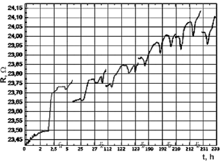
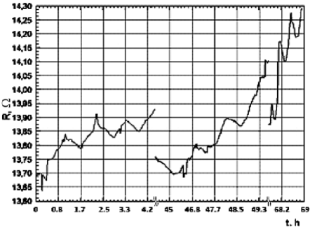
Experimentally, we studied two specimens: a specimen, which was elastically deformed beforehand by applying a squeezing force of 55 MPa (specimen 2) and a specimen, which was not preliminarily subjected to a deformation (specimen 2). In Figs. 3 and 4, the variations in the dependences of the specimen electroresistances on the elastic strain time and the specimen annealing duration at room temperature are shown for both specimens. The results of experiments in the course of a single “squeezing–strain relief” cycle are presented by a solid curve; the break between the curves indicates the holding of the specimen after the previous “squeezing–strain relief” cycle (for the break duration, see the figure caption). The cycle following the holding corresponds to the following plot interval (a solid curve), the initial section of which (the resistance growth) corresponds, as a rule, to the squeezing stage, and the following recession stage corresponds to the strain relief. These dependences make it evident that (i) the magnitude of residual specimen electroresistance grows from cycle to cycle, with the intensity of this growth decreasing after several cycles; (ii) in the specimen preliminarily subjected to a deformation, the processes that are responsible for the gradual increase in the specimen electroresistance are slowed down; (iii) after the mechanical loading relief and the holding of the specimen at room temperature for not more than an hour, the specimen demonstrates a slow growth of its electroresistance; and (iv) holding the specimen at room temperature for 24 h and longer gives rise to a partial restoration of its conductance.
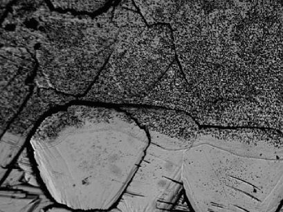
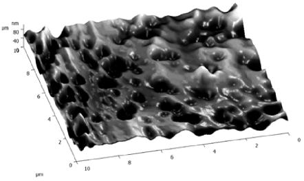
The structural researches consisted in a microscopic examination of the specimen surface state after the selective etching. Figure 5 shows the photos obtained on an optical microscope. They demonstrate that an increased concentration of defects is formed under the sputtered film after the processes of squeezing and strain relief. The analysis of the photos (Fig. 6) of the selectively etched surface obtained with the use of atomic force microscopy testifies that those defects are groups of structural surface defects that differ from dislocation etching pits by their depth and edge shape. The authors of work [10] regarded those defects as the clusters of point defects.
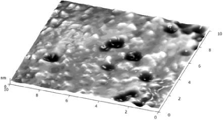
At the same time, such an increase in the defect concentration was not observed on the substrates of crystals with sputtered Al films but not subjected to the action of any external force (Fig. 7). This fact allows us to assert that those defects were gettered in the near-surface layer of the crystal from the crystal bulk, as a result of the external strain and the presence of the Al film.
Since dislocations create a field of mechanical stresses around themselves, they are efficient drains for any defects or impurities in the crystal. When an external mechanical field is applied to the specimen, dislocations can wander through the lattice (in particular, loop-like dislocations with fixed ends are capable of bending), so that an additional capture of defects from the crystal bulk takes place. In the case of uniaxial crystal strain, dislocations approach the near-surface layer with mechanical stresses induced by a mismatch between the lattice parameters of silicon and aluminum film, and defects localized around the dislocation core become captured in the disturbed near-surface layer. This model explains a variation of the specimen conductance during a deformation. If the loading decreases, the dislocation gets straight and returns back to the initial position, whereas some captured defects remain in the deformation potential field induced by the lattice parameter mismatch. As a result, the specimen resistance changes between the deformation cycles.
The defect wandering through the lattice can induce the appearance of traps that can capture charge carriers. The filling of those traps is accompanied by a reduction in the concentration of charge carriers and, respectively, in a growth of the specimen resistance after the deformation has been terminated. The role of such defects can be played by dislocations that release the captured defects to the near-surface layer, by vacancies taken out by dislocations to the surface, and so forth.
However, the explanation of the variation in the specimen electroconductance is not limited to a single mechanism. The blocking of donor centers that have arisen or shifted in the course of deformation is also possible. One more mechanism consists in a variation of the magnitude of charge carrier scattering by defects taken out to and captured in the near-surface layer.
After carrying out the researches dealing with the level-by-level etching of the surface, we obtained a layer with the concentration of etching pits equal to the initial value (before the sputtering of the Al film). In such a way, we experimentally determined the maximum depth of probable defect capture by the near-surface deformed layer, which turned out to equal 1.5 . This value coincides with the theoretically calculated one to within the calculation error.
5 Conclusions
The sputtering of a metal film onto the silicon substrate and the subsequent elastic strain of the latter result in the defect capture from the crystal bulk in the near-surface deformed layer. Our calculations showed that the near-surface layer of silicon is deformed owing to the mismatch between the lattice parameters in the crystal and the film. As a result, there emerges a deformation potential near the surface, which promotes the defect capture (the Cottrell atmosphere) from dislocations that approach the surface under the action of an external elastic strain. The analysis of the microscopic structure of the surface showed that those defects are the clusters of point defects. Possible mechanisms of the influence of the elastic strain on the crystal electroconductivity by means of increasing the defect concentration in its near-surface region are described. Theoretical calculations for the energy distribution across the deformed near-surface layer and the energy of dislocations are carried out, and the maximum depth of probable defect capture is found, which correlates well with the experimentally obtained results.
References
- [1] R. Chau, S. Datta, M. Doczy et al., IEEE Electr. Dev. Lett. 25, 408 (2004).
- [2] O.M. Kanunnikova, V.I. Kozhevnikov, and O.Yu. Goncharov, Khim. Fiz. Mezoskop. 10, 63 (2008).
- [3] P.N. Krylov, Vestn. Udmurt. Univ. 4, 125 (2006).
- [4] B.V. Pavlyk, R.I. Didyk, D.P. Slobodzyan et al., Fiz. Khim. Tverd. Tila 10, 783 (2009).
- [5] V.N. Vigdorovich, A.E. Vol’pyan, and G.M. Kurdyumov, Directional Crystallization and Physico-Chemical Analysis (Moscow, Khimiya, 1976) (in Russian).
- [6] Ch. Kittel, Introduction to Solid State Physics (Wiley, New York, 1995).
- [7] G.I. Epifanov, Solid State Physics (Vysshaya Shkola, Moscow, 1980) (in Russian).
- [8] V.G. Kotlyar, A.A. Saranin, A.V. Zotov et al., Vestn. Dalne-Vost. Otdel. RAN 1, 103 (2005).
- [9] L.D. Landau and E.M. Lifshitz, Theory of Elasticity (Pergamon Press, New York, 1959).
-
[10]
B.V. Pavlyk, R.I. Didyk, Y.A. Shykorjak et al., Teor.
Elektrotekhn. 61, 164 (2010).
Received 25.06.12.
Translated from Ukrainian by O.I. Voitenko
Б.В. Павлик, М.О. Кушлик, Р.I. Дiдик,
Й.А. Шикоряк, Д.П.
Слободзян, Б.Я. Кулик
ЕЛЕКТРОФIЗИЧНI ХАРАКТЕРИСТИКИ
ПРИПОВЕРХНЕВИХ ШАРIВ КРИСТАЛIВ Si
-ТИПУ, З НАПИЛЕНИМИ ПЛIВКАМИ
Al,
ПIДДАНИХ ПРУЖНIЙ ДЕФОРМАЦIЇ
Р е з ю м е
Показано, що осаджена плiвка Al
на поверхню (111) кристала Si() формує деформацiйне поле в
приповерхневому шарi. За одновiсної пружної деформацiї кристала
спостерiгається гетерування дефектiв з об’єму зразка у
приповерхневому шарi пiд напиленою плiвкою. Отримана залежнiсть
змiни величини опору цих зразкiв вiд величини пружної деформацiї
пiдтверджує гетерування електрично активних дефектiв у
приповерхневому деформованому шарi. Проведено теоретичнi розрахунки
максимальної глибини захоплення цих дефектiв на основi енергiї
взаємодiї деформованого шару та дислокацiй.