Grain boundary ferromagnetism in vanadium-doped In2O3 thin films
Room temperature ferromagnetism was observed in In2O3 thin films doped with 5 at.% vanadium, prepared by pulsed laser deposition at substrate temperatures ranging from 300 to 600 . X-ray absorption fine structure measurement indicated that vanadium was substitutionally dissolved in the In2O3 host lattice, thus excluding the existence of secondary phases of vanadium compounds. Magnetic measurements based on SQUID magnetometry and magnetic circular dichroism confirm that the magnetism is at grain boundaries and also in the grains. The overall magnetization originates from the competing effects between grains and grain boundaries.
Qi Feng111Present address: SKLSM, Institute of Semiconductors, Chinese Academy of Sciences, P. O. Box 912, Beijing 100083, People’s Republic of China, Harry J Blythe, A Mark Fox, and Gillian A Gehring222g.gehring@sheffield.ac.uk
Department of Physics and Astronomy, The University of Sheffield, S3 7RH, UK
Xiu-Fang Qin, and Xiao-Hong Xu
School of Chemistry and Materials Science, Shanxi Normal University, Linfen 041004, People’s Republic of China
Steve M Heald
Advanced Photon Source, Argonne National Laboratory, Argonne, Illinois, 60439, USA
Keyword:Dilute Magnetic Oxide, Magnetism, Magnetic Circular Dichroism, Grain Boundaries
1 Introduction
Dilute magnetic oxides (DMOs) have been identified as one of the most attractive materials for future spintronics applications [1, 2, 3, 4]. However the field has also been very controversial. In some cases the magnetism has been attributed to ferromagnetic nano-inclusions [5, 6] although there have been a number of cases where the magnetic properties were identified in samples without any impurity phases leading to the conclusion that a ‘non-trivial defect-related’ ferromagnetic phase exists in some oxides [7]. The possible explanations of oxide magnetism were further limited by the X-ray magnetic circular dichroism experiment which showed that Co ions in ZnCoO were themselves paramagnetic [8]; this startling result has been confirmed by further investigations of other doped magnetic semiconductors [9, 10, 11, 12]. In addition, large magnetic moments have also been observed in undoped oxides [13]. This has meant that acceptable models should now include those where the magnetism is associated with electrons in states other than on the transition-metal (TM) ions themselves.
Another feature of TM-doped oxide materials is that ferromagnetism (FM) is absent in epitaxial films and in the bulk, this was quantified by Straumal et al [14, 15] who proposed a model of grain boundary (GB) FM in pure and doped ZnO. They found that FM only occurred if the grains were sufficiently small where , the critical grain size, was increased if Mn was doped into ZnO, a similar effect has been seen in Mn-doped In2O3 [16]. Coey [17] proposed that the FM originates from a narrow spin split defect band whose population is controlled by doping TM ions. There are two obvious candidates for such a band: it might arise from states localized at the grain boundaries as suggested by the work of Straumal et al [14, 15] or it might be the narrow band originating from states at oxygen vacancies as had been proposed earlier for both ZnO and In2O3 [18]. This letter investigates the effects of the grains and the GBs on the overall magnetization in V-doped In2O3 thin films.
In2O3 is a promising candidate material to exhibit strong GB magnetism because there is electron accumulation at the surfaces of pure In2O3 grains [19, 20] and it can also be grown strongly oxygen-deficient. There have been a number of studies of doped In2O3 following the initial identification of strong magnetism for Cr doping [21]. FM has been seen for doping with Mn [22], Fe [23, 24], Co [25], V [26] and also in undoped, but oxygen-deficient, In2O3 [13] and as a surface effect in ITO [27, 28]. Vanadium is interesting and a good dopant for our study because V3+ can substitute for In3+, however its smaller ionic radius (78pm) compared with (94pm) for In3+ will cause local strains and enhance the formation of GBs; it has been shown to be strongly ferromagnetic in In2O3 [26] in spite of the fact that it does not form compounds with In and O that are ferromagnetic at room temperature.
In this letter we describe measurements on a series of V-doped In2O3 films that were fabricated such that they had different grain sizes. In order to investigate the origin of the observed FM, we measured the structural, magnetic, electrical, optical and magneto-optical properties of V-doped In2O3 films. X-ray diffraction (XRD) measurements allow us to estimate the preferred orientation, grain size, whereas the structural perfection around the TM site is studied by extended x-ray absorption fine structure (EXAFS). Magnetic properties were characterized by SQUID magnetometry which detects contributions from both spin and orbital magnetism and by magnetic circular dichroism (MCD), which is a powerful tool to confirm the energy of the magnetic states that give rise to the magnetism but since it is due to electric dipole transitions only detects orbital moments [29, 30, 31]. We show that the overall magnetism originates from both the grains and the GBs in this material. The samples with smaller grain size have larger magnetization but a smaller MCD signal, whereas the samples with with a larger grain size have a smaller magnetization but larger MCD signal; this is due to the different contribution of the orbital magnetism in the two components.
2 Experiment
Polycrystalline thin films of (In0.95V0.05)2O3 were deposited on -cut sapphire substrates at temperatures ranging between 300 and 550 in 10-5 Torr of oxygen by pulsed laser deposition (PLD) with a XeCl laser (308 nm). The laser was used at a pulse repetition rate of 10 Hz, which gave an energy density up to 400 mJ/pulse. The target-to-substrate distance was 40 mm. Bulk targets for ablation were prepared by a standard solid-state reaction routine, as described elsewhere [32]. Phase identification and structural properties of all the films were characterized by XRD on a Bruker diffractometer in the -2 mode using Cu radiation ( = 1.5406 Å). X-ray absorption fine structure (XAFS) measurements were performed at beamline 20-ID-B at the Advanced Photon Source using a microfocused beam incident on the sample at approximately 5∘ glancing angle. The magnetization measurements were performed in a SQUID magnetometer. The thickness of the films was measured with a Dektak profilometer and was kept almost constant at 120 10 nm. Temperature dependence of the resistance and Hall effect measurements were performed in the Van der Pauw geometry, in a continuous-flow helium cryostat in the range 5 - 300 K in fields up to 1 T. Optical absorption spectra and magneto-optical spectra were measured in Faraday geometry by using a photo-elastic modulator from 2.0 eV to 3.5 eV in fields up to 1.8 T. Since this energy range is below the band-gap of In2O3, the magneto-optical response probes the magnetic polarization of any gap states.
2.1 Structural Properties
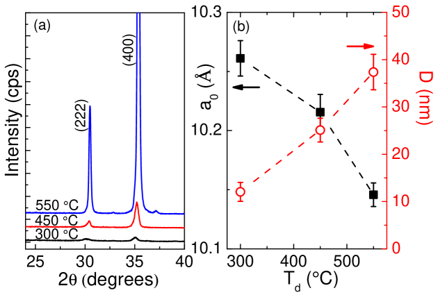
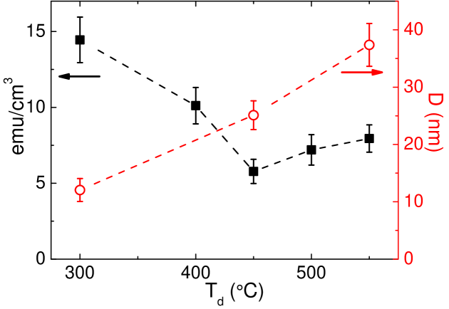
Fig.1(a) shows the XRD scans of (In0.95V0.05)2O3 films. All peaks were indexed assuming the same bixbyite cubic structure as pure In2O3. No evidence of any secondary phases of V was observed within the detection limit. As shown in Fig.1(b), the lattice constant was found to decrease as the deposition temperature increases, which is due to the smaller ionic radius of V3+ (78 pm) compared with that of In3+ (94 pm); this suggests that more V ions are incorporated into the host lattice as the deposition temperature increases. The average size of the crystalline grains, , in the films was estimated using the Debye-Scherrer method, , where is the wavelength of the x-ray, the full width at half maximum of (222) peak and the diffraction angle. The grain size was found to increase with substrate temperature, shown in Fig.1(b), from 12.5 to 34.4 nm for V-doped films.
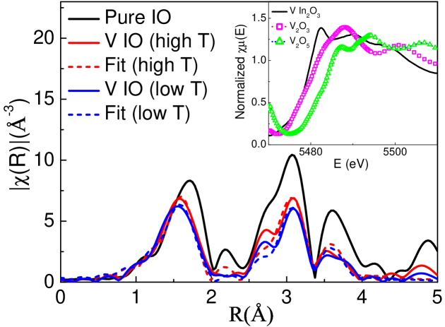
XAFS measurements were used to look for potential second phase formation. An analysis was carried out that was very similar to that described earlier [33]. As seen in the inset in Fig.2, the position of the near edge of V clearly indicates that all of the V is in the 3+ valence state. EXAFS is used to explore the local environment of the doped TM ions. Fig.2 shows the Fourier transformed data for pure In2O3 and two V-doped In2O3 films, which were grown at 300 and 550 . As shown earlier [33], the dopant sites in the In2O3 lattice can have widely varying degrees of disorder. The V data can be well-fitted, suggesting that V occupies substitutional sites, as shown in Fig.2. To fit the data, we initially used a two-site model [33], which gave a good fit to all V data, although there is a mismatch near Å. The fit could not be significantly improved by the addition of secondary phases, such as metal V, VO, VO2, V2O3. Therefore, we suggest that this mismatch may be due to distortion around the V site, such as GBs. Reduced disorder in the data for the film grown at 550 suggested that the crystallinity in the neighborhood of the V ions was improved by growth at a higher temperature as found by XRD.
2.2 Optical Properties
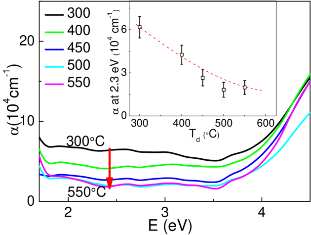
Fig.3 shows the optical absorption, together with the surface scattering measurements at room temperature as a function of photon energy for V-doped In2O3 films grown at different temperatures. The transmittance below the band gap is found to increase with increase in substrate temperature. The absorption in the low energy region decreases significantly with increasing substrate temperature, as shown in the inset in Fig.3. Thus, the optical data support the EXAFS and the conclusions drawn from the XRD that, as deposition temperature increases, the crystallinity improves and grain size increases. Similar behavior was observed for Mn- and Fe-doped In2O3 films [16].
2.3 Electrical Properties
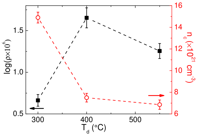
Measurements of the Hall effect and the resistivity were performed in Van der Pauw geometry at both 5 and 300 K to explore the carrier concentration, and resistivity. The films show metallic behaviour over the temperature range 5T300 K. The room temperature resistivity, , and the carrier concentration, , for V-doped In2O3 films as a function of deposition temperature for V-doped In2O3 films are presented in Fig.4. The carrier concentration was comparable to that found for undoped In2O3 films grown at low oxygen pressure. Further experiments will be required to investigate if the electrons that are localized at the GBs carry an appreciable fraction of the total current in the material.
2.4 Magnetic Properties
| D | at 2.3 eV | MCD at 3.3 eV | ||||
| () | (nm) | (nm) | (104 cm-1) | (degrees/cm) | ( emu) | (emu/cm3) |
| 300 | 115 5 | 12.1 0.1 | 6.2 0.3 | 220 25 | 3.2 0.3 | 14.5 1.3 |
| 400 | 115 5 | - | 4.3 0.2 | 230 25 | 2.3 0.2 | 10.1 0.9 |
| 450 | 125 5 | 25.1 0.2 | 2.7 0.1 | 980 75 | 1.4 0.1 | 5.8 0.5 |
| 500 | 125 5 | - | 1.8 0.1 | 660 65 | 1.8 0.1 | 7.2 0.7 |
| 550 | 110 5 | 37.4 0.2 | 2.0 0.1 | 1130 80 | 1.6 0.1 | 7.9 0.2 |
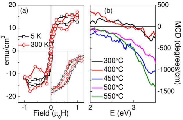
Magnetic properties were investigated by SQUID magnetometry, the data shown in this letter has been analyzed by subtracting the diamagnetic contribution of the pure sapphire substrate. Fig.5(a) shows the in-plane M-H curves of V-doped In2O3 films at 5 and 300 K. The temperature independent magnetization in this case and all the other TM-doped In2O3 samples agrees with that found in Fe-doped In2O3 films by Jiang et al [34] and Park et al [35]. They found that for Fe-doped In2O3 thin films, magnetization was temperature independent in a metallic sample, whereas temperature dependent magnetization was observed in a semiconducting sample. Fig.5(b) shows the room temperature MCD as a function of photon energy for V-doped In2O3 films. The MCD spectra, together with the saturation magnetization, was unchanged down to 10 K indicating a lack of signal from any V minority phases.
Fig.6 shows the saturation magnetization and the grain size as a function of deposition temperature for V-doped In2O3 thin films. It is clear that as the deposition temperature increases, the grain size increases, whereas the saturation magnetization decreases. Information of the thickness, , grain size, , loss coefficient, , saturation magnetization, , and MCD for samples prepared at different substrate temperature, , is summarized in table 1. The saturation magnetization was analyzed in terms of the thickness and the surface area of the sample; surface area is almost constant during the PLD process, about 20 mm2 and the thickness of samples was kept almost constant at 120 nm. In Ref [27], it was found that undoped In2O3 had a moment of 0.5 emu/cm3 which is small compared with the values found here 2-15 emu/cm3. It is important to note that our results are significantly large compared also with other published results which means that our values are more robust [13, 21, 27].
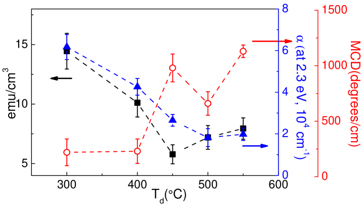
Fig.7 shows the variation of the room temperature saturation magnetization, MCD and optical absorption coefficient for V-doped films, as a function of substrate temperature. The saturation magnetization decreases as a function of deposition temperature, behaving similarly to the optical absorption. This shows that when the grain size gets larger at higher deposition temperature, the scattering from the sample surface becomes weaker, thus leading to smaller absorption; this is in consistent with measurements of D found from XRD. More grain boundaries form with smaller grain size in the normalized volume. The decrease of saturation magnetization as the grain size increases strongly suggests that much of the observed magnetism originates from the grain boundaries.
The MCD values quoted in Fig.7 were measured at 3.3 eV, which is just below the band-gap; this is believed to correspond to transitions to spin-polarized gap states. The MCD signal would be zero if the magnetization were zero, but they are not necessarily proportional because of the importance of spin-orbit coupling. The MCD spectra shown in Fig.5(b) peak at the band edge as expected for an oxide but actually fall into two distinct groups. There is a small dispersive signal for the samples grown at 300 and 400 , where the samples have a high magnetization, and a larger absorption-like signal for the higher temperatures where the magnetization is reduced. These spectra are similar to those found for Mn and Fe-doped In2O3 [16]. The Mn-doped sample had a high magnetization when grown at low temperatures and the MCD spectrum was dispersive. The maximum magnetization for the Fe-doped sample occurred for high growth temperature and this was accompanied by an absorptive MCD spectrum. The magnitude of the absorptive MCD spectrum for Fe was much larger than that for the dispersive signal for Mn, even though the magnetization was significantly higher for Mn.
The MCD depends on a change in the angular momentum in the optical transitions and this is related to the observed magnetization via the spin-orbit coupling. For any one material the MCD follows the magnetization as a function of temperature or magnetic field. However, for different materials, the magnitude of the MCD also depends on the spin-orbit coupling that is necessary to induce an orbital moment. For the purposes of this discussion boundary magnetism and grain magnetism are two different quantities. Thus it appears that the magnetism located at grain boundaries arises from electrons with rather weak spin-orbit coupling hence a large grain boundary magnetism gives a small MCD signal. On the other hand the electrons that cause the magnetism in the grains have a much larger spin-orbit interaction and hence a large MCD signal may be generated by a smaller magnetization. These results are strong evidence to support the contention that the observed FM originates from both the grain boundaries and the grains. We note that the magnetization from the grains increases when the grains form a larger fraction of the whole sample and also the concentration of V ions has increased as indicated by the change in lattice constant observed by XRD.
The large from the boundaries has a relatively low orbital contribution and hence gives a small MCD signal. As the grains get larger the grain contribution begins to be more important and this has a larger orbital contribution and hence gives a relatively large MCD. The GB FM, however, dominates in the samples.
3 Conclusion
In conclusion, we have observed room temperature FM in V-doped In2O3 films by SQUID and MCD measurements. The increase in grain size with deposition temperature was observed in doped films, similar to that found in Mn- and Fe-doped films [16]. Structural characterization indicated V ions are substituted at the In sites in the In2O3 host, and more V ions were incorporated into the host lattice at higher deposition temperature. Although the fit to the EXAFS data shows some mismatch, the existence of secondary phases of V was excluded. The contribution from secondary phases in doped films was also excluded by low temperature MCD measurements. The large magnetization seen for V-doped samples, when the grains were small indicates that GB FM is observed in V-doped In2O3 films, similarly to that found in Mn-doped ZnO and In2O3 films [14, 16], as a growing evidence of GB model. The magnetization of V-doped samples is relatively large compared with other oxide materials - it may be significant that unlike Mn, Co which are present as divalent ions and Fe where magnetization depends on having some divalent Fe [34] as well as trivalent Fe the V ions are all V3+ and yet the magnetization is unusually large. The system with Gb FM would be a promising source of spin-polarized currents if the electrons that are polarized at the GBs carry an appreciable fraction of the total current in the material. Therefore further investigation is required.
Acknowledgement
Use of the Advanced Photon Source, an Office of Science User Facility operated for the U.S. Department of Energy (DOE) Office of Science by Argonne National Laboratory, was also supported by the U.S. DOE under Contract No. DE-AC02-06CH11357. The work is also financially supported by NSFC (51025101).
References
- [1] Wolf S A, Awschalom D D, Ruhrman R A, Daughton J M, Vonon Molnár S, Roukes M L, Chtchelkanova A Y and Treger D M 2001 Science 294 1488
- [2] Žutić I, Fabian J and Sarma S D 2004 Rev. Mod. Phys. 76 323
- [3] Coey J M D, Venkatesan M and Fitzgerald C B 2005 Nat. Mater. 4 173
- [4] Bader S and Parkin S 2010 Annu. Rev. Cond. Mat. Phys. 1 71
- [5] Kim D H et al 2002 Appl. Phys. Lett. 81 2421
- [6] Heald S M et al 2009 Phys. Rev. B 2009 79 075202
- [7] Coey J M D 2006 Curr. Opin. Solid State Mater. Sci. 10 83
- [8] Tietze T, Gacic M, Schütz G, Jakob G, Brück S and Goering E 2008 New J. Phys. 10 055009
- [9] Barla A, Schmerber G, Beaurepaire E, Dinia A, Bieber H, Colis S, Scheurer F, Kappler J P, Imperia P, Nolting F, Whilhelm F, Rogalev A, Müller D and Grob J J 2007 Phys. Rev. B 76 125201
- [10] Ney A et al 2010 New J. Phys. 12 013020
- [11] Hakimi A M H R, Schoofs F, Bali R, Stelmashenko A, Blamire M G, Langridge S, Cavill S A, Laan van der and Dhesi S S 2010 Phys. Rev. B 82 144429
- [12] Saki E, Amemiya K, Chikamatsu A, Hirose Y, Shimada T and Hasegawa T 2012 J. Magn. Magn. Mater. 323 130
- [13] Hong N H, Barla A, Sakai J and Huong N Q 2007 physica status solidi(c) 4 4461
- [14] Straumal B, Mazilkin A, Protasova S, Myatiev A, Straumal P, Schtz G, van Aken P, Goering E and Baretzky B 2009 Phys. Rev. B 79 205206
- [15] Straumal B B, Protasova S G, Mazilkin A A, Schütz G, Goering E, Baretzky B and Straumal P B 2013 JETP Letters 97 367
- [16] Feng Q, Blythe H J, Jiang F X, Xu X H, Heald S M, Fox A M and Gehring G A, accepted in APL Materials
- [17] Coey J M D, Stamenov P, Gunning R D, Venkatesan and Paul K 2010 New J. Phys 12 053025
- [18] Lany Stephan and Zunger Alex 2007 Phys. Rev. Lett. 98 045501
- [19] King P D C, Veal T D, Payne D J, Bourlange A, Egdell R G and McConville C F 2008 Phys. Rev. Lett. 101, 116808
- [20] King P D C, et al. 2009 Phys. Rev. B 79 205211
- [21] Philip J, Punnoose A, Kim B I, Reddy K M, Layne S, Holmes J O, Satpati B, LeClair P R, Santos T S and Moodera J S 2006 Nat. Mater. 5 298
- [22] Jiang F X, Xu X H, Zhang J, Fan X C, Wu H S and Gehring G A 2010 Appl. Phys. Lett. 96 052503
- [23] Jiang F X, Xu X H, Zhang J, Wu H S, Gehring G A 2009 Applied Surface Science 255 3655
- [24] Xu X H, Jiang F X, Zhang J, Fan X C, Wu H S and Gehring G A 2009 Appl. Phys. Lett. 94 212510
- [25] Hakimi A M H R, Blamire M G 2011 Phys. Rev. B 85 085201
- [26] Gupta A, Cao H T, Parekh K, Rao K V, Raju A R and Waghmare U V 2007 J. Appl. Phys. 101 09N513
- [27] Panguluri R P, Kharel P, Sudakar C, Naik R, Suryanarayanan R, Naik V M, Petukhov A G, Nadgorny V and Lawes G 2009 Phys. Rev. B 79 165208
- [28] Xia B, Wu Y, Ho H W, Ke C, Song W D, Huan C H A, Kuo J L, Zhu W G and Wang L 2011 Physica B 406 3166
- [29] Neal J R, Behan A J, Ibrahim R M, Blythe H J, Ziese M, Fox A M and Gehring G A 2006 Phys. Rev. Lett. 96 197208
- [30] Hakimi A M H R, Banerjee N, Aziz A, Robinson J W A and Blamire M G 2010 Appl. Phys. Lett. 96 102514
- [31] Gehring G A, Alshammari M S, Score D S, Neal J R, Mokhtari A and Fox A M 2012 J. Magn. Magn. Mater. 324 3422
- [32] Hasan, et al., in preparation
- [33] Heald S M, Alshammari M S, Alfehaid S, Alotaib M, Feng Q and Hakimi A M H R 2013 J. Physics: Conference Series 430 012081
- [34] Jiang F X et al. 2011 J. Appl. Phys. 109 053907
- [35] Park C Y, You C Y, Jeon K R, Shin S C 2012 Appl. Phys. Lett. 100 222409