Electric Field Effects on Armchair MoS2 Nanoribbons
Abstract
Abstract
Ab initio density functional theory calculations are performed to investigate the electronic structure of MoS2 armchair nanoribbons in the presence of an external static electric field. Such nanoribbons, which are nonmagnetic and semiconducting, exhibit a set of weakly interacting edge states whose energy position determines the band-gap of the system. We show that, by applying an external transverse electric field, , the nanoribbons band-gap can be significantly reduced, leading to a metal-insulator transition beyond a certain critical value. Moreover, the presence of a sufficiently high density of states at the Fermi level in the vicinity of the metal-insulator transition leads to the onset of Stoner ferromagnetism that can be modulated, and even extinguished, by . In the case of bi-layer nanoribbons we further show that the band-gap can be changed from indirect to direct by applying a transverse field, an effect which might be of significance for opto-electronics applications.
Over the past several years one dimensional (1D) nanostructures, such as nanotubes, wires, rods, belts and ribbons have attracted a growing interest from researchers keen to investigate the wide array of photophysical, photochemical and electron-transport properties that are unique to their dimensionality.review_1D_2003 ; ACS_Ich_2006_45 The study of these nanostructures has also been facilitated by recent advances in nano-lithographic techniques,review_AdvP_3 such as electron beam or focused-ion-beam (FIB) writing review_AdvP_4a ; review_AdvP_4b and X-ray or extreme-UV lithography,review_AdvP_5 whereby such 1D systems can be readily fabricated in the research laboratory. From a nanotechnology perspective, 1D structures offer a range of potential applications that are different from those provided by their 2D and 3D counterparts.review_1D_2003 ; review_AdvP_1
While carbon nanotubes (CNTs) remain the most widely studied 1D nanostructures to date, nanowires (NWs) and nanoribbons (NRs) have lately received increasing attention as possible alternatives. In particular the fact that the electronic structure of NRs can be modified by manipulating their edges, which usually are more reactive than the bulk, offers a powerful tool for customizing such nanostructures to a particular application. For this reason recent times have witnessed an explosion of theoretical and experimental studies on NRs. Primarily these have been devoted to graphene NRs (GNRs),PRB_54_17954 ; PRB_59_8271 ; PRL_2007_98 but many other materials have been either made or predicted in the NR form. These include BC3,APL_2009_94 ; JACS_133_16285 BN,NL_2008_8 ; NL_2008_8_2 ; NL2011113221 ZnO,Pan_2001 ; ChPL_2007_448 ; ACS_Nano_2010_4 Si,JACS_123_11095 ; APL_2009_95 etc. Intriguingly for some of these a magnetic ACS_Nano_2010_4 ; APL_2009_95 or even a half-metallic ground state has been predicted.PRB_2008_78
This work investigates MoS2 NRs, which represent one of the several low-dimensional structures that can be made from transition-metal dichalcogenides. Layered transition-metal dichalcogenides are particularly interesting because of the large variety of electronic phases that they can exhibit,ReviewMoS2-1 ; ReviewMoS2-2 namely metallic, semiconductor, superconductor and charge density wave. Bulk MoS2 has a prototypical layered structure where Mo is covalently bonded to S with a trigonal prismatic coordination. Each S-Mo-S sandwich layer is tightly bound internally and interacts weakly with the neighboring sandwich only through van der Waals forces.SSCom_1972_11 Because of such a structure the fabrication of ultrathin crystals of MoS2 is possible by micro- mechanical cleavage PNAS_2005_102 or exfoliation.JNC_2011 Therefore, like graphene,Sc_2004_306 single layers of MoS2 can be extracted repeatedly one by one from bulk materials and deposited on substrates for further studies.arxive_1
From the parental MoS2 single-layer crystal several nanostructures can be made. These have been traditionally studied in the context of catalysis for desulfurization processes NatNanoT_2007_2 ; Jcat_2007_249 and as thermoelectric materials.JPChemC_2007_111 Here we explore a different aspect, namely how the electronic properties of MoS2 armchair nanoribbons (ANRs) can be manipulated by the application of an external electric field, . In particular we look at the possibility of inducing a metal-insulator transition in the nanoribbons, and at the associated magnetic moment formation via the Stoner mechanism in the search for a large magneto-electric effect. Our study thus complements those already reported in the literature for graphene,nature_2006_444 BN,NL_2008_8 BC3 APL_2009_94 and AlN.CPL_2009_469
The paper is organized as follows. In the next section we present a description of the various structures investigated. The calculated electronic properties of bulk and single layer MoS2 as well as several ANRs are discussed in the following section. First we analyze single layer MoS2 ANRs and present results from non spin-polarized calculations including an applied static electric field. These are explained by means of a simple tight-binding model. Then the electronic structure and the electric field response of bilayer and multi-layer ANRs are presented. Finally we show results obtained from spin-polarized calculations investigating magneto-electric effects in single layer MoS2-ANRs and, before concluding, we consider the effects that different edge terminations have on the electric field driven magnetism.
NANORIBBONS STRUCTURE
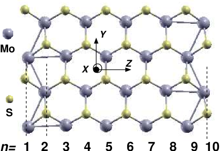
Bulk MoS2 has a hexagonal crystal structure with space group P63/mnc (D) and it is the 2D template for constructing the NRs. Similarly to C nanotubes,nature_injma MoS2 NRs may be described by the 2D primitive lattice vectors and of the parental 2D structure and two integer indices ,PRL_68_1597 so that the chiral vector is defined as . Three types of NRs can thus be identified: zig-zag for , armchair for , , and chiral for . MoS2 ANRs are nonmagnetic semiconductors irrespective of their size, whereas the zig-zag nanoribbons (ZNRs) are predicted metallic and magnetic.JACS_2008_130 Since our goal is that of describing an electric-field induced metal-insulator transition our starting point must consist in NRs with an insulating ground state. As such we consider only ANRs. As a matter of notation, following several previous studies,JACS_2008_130 ; NL_2008_8 ; NLStefano we identify the different sized MoS2 ANRs as -ANR, where is the number of dimer lines across the terminated direction of the 2D MoS2 layer, i.e. across the non-periodic dimension of the nanoribbon (see Fig. 1). The multilayer ribbons are constructed by placing single layer ribbons on top of each other with an ABA stacking.PRB_2009_79
RESULTS AND DISCUSSION
Electronic properties
Our systematic study begins with calculating the electronic properties of MoS2 in its bulk form. The optimized bulk MoS2 unit cell parameters are Å, , while the S-Mo-S bonding angle is 82.64∘. These values are in good agreement with previous theoretical calculations PRB_2001_64_235305 and also with the experimental ones of Å, .JPCM_1992_4 The Mo-S bond length in bulk MoS2 is found to be 2.42 Å, again in close agreement with the experimental value of 2.41 Å JPCM_1992_4 and to the earlier theoretical estimate of 2.42 Å.ReviewMoS2-1 Bulk MoS2 is a semiconductor and we predict an indirect band gap of 0.64 eV between the point and a point half way along the -K line. Our calculated band-gap is smaller than the experimental one of 1.23 eV, PRB_2001_64_235305 ; JPCM_1992_4 but it is in good agreement with existing density functional theory (DFT) calculations at the local spin density approximation (LSDA) level.PRB_2001_64_235305 ; PRB_1995_51 It is well known that the LSDA systematically underestimates the band-gap, so that such result is not surprising. However, we note here that the LSDA underestimation affects our results only at a marginal quantitative level.
Next we move to study the electronic properties of a single MoS2 layer. Our optimized lattice constant, , is now 3.132 Å, i.e. it is slightly smaller than that in the bulk. Such value is in close agreement with the experimentally observed one of 3.15 Å.PRL_2000_84 Our calculations show that as the number of layers is decreased from the bulk to a few layers, the minimum of the lowest unoccupied band shifts from half way along the -K line to K, with a single MoS2 layer exhibiting a direct band-gap at K. In this context, recent experiments NL_2010_10 ; PRL_2010_136805 have shown that as the thickness of layered MoS2 samples decreases from the bulk towards the monolayer limit, photoluminescence emerges, indicating the transition from an indirect to a direct band-gap. A similar conclusion was reached by comparing scanning photoelectron microscopy to DFT calculations.PRB_2011_045409 Both for the bulk and the single layer the band structure around the Fermi level, , is derived mainly from Mo-4 orbitals, although there are smaller contributions from the S-3 via hybridization within the layer.
In Fig. 1 the optimized geometry of a MoS2 10-ANR is shown (the periodicity is along the -direction). For symmetric ANRs ( odd) the two edges have mirror refection symmetry, while this is not the case for the antisymmetric ones ( even). Our calculations show that the two possible ribbon configurations are essentially energetically degenerate, meaning that the total energy per atom scales with the ribbon size but does not depend on the ribbon symmetry. We have then checked that the electronic properties and their dependence on the external electric field are insensitive to the ribbon geometry and here we present data only for the asymmetric case.
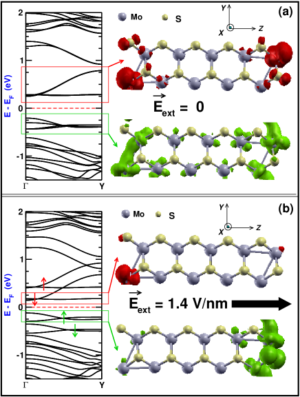
In order to determine the ground state of the different -ANRs, we have first carried out both spin-unpolarized and spin-polarized total energy calculations including geometry optimization. We take the case of a 10-ANR as an example and we use its electronic structure to discuss the general properties of such a NRs class. From the bandstructure [shown in Fig. 2(a)], it is clear that a 10-ANR is a non-magnetic semiconductor with a direct (LSDA) band-gap of 0.45 eV at the point. This is in agreement with previous calculations.JACS_2008_130 The local density of states (LDOS) of the conduction band (CB) and valence band (VB) [shown in Fig. 2(a)] indicates that the electronic states around are completely localized at the ANR’s edges. The CB and the VB originate from a hybridized mix of Mo-4 and S-3 orbitals with the hybridization being stronger in the VB than in the CB.
Such results are relatively independent of the ribbon size, and unlike graphene NRs, all the MoS2 ANRs are semiconducting. For the smaller -ANRs (), the band-gap oscillates in magnitude with increasing and finally converges to a constant value of around 0.52 eV for larger sized ribbons (). The same oscillatory behaviour has been observed in earlier calculations JACS_2008_130 and it is quite similar to that predicted for BN-ANRs.NL_2008_8_2 As increases we also observe oscillations in the equilibrium lattice constant, which slowly approaches a constant value of 3.132 Å, similar to that calculated for the infinite MoS2 single layer. We thus note that the calculated band-gaps for all -ANRs are much smaller than that of the infinite MoS2 single layer (1.90 eV), while the lattice constants deviates only marginally. The reason for such a difference is rooted in the fact that both the VB and CB of the ribbons are formed by states strongly localized at the two edges. Indeed these states do not exist in the case of the infinite MoS2 single layer and they are simply a consequence of the different wave-function boundary conditions.
Response of a MoS2-ANR to
We now discuss the response of the electronic structure of the MoS2-ANRs to a static external electric field, . As mentioned earlier, the size of the ribbon band-gap is determined by the energy position of the edge states forming the CB and the VB. Thus any change in the ANR band-gap under an applied field would be mainly determined by the response of its edge states. It is worth noting that for , both the CB and VB are doubly degenerate as there are two states in each band corresponding to the two edges of the ribbon (this means that the electron density corresponding to either the CB or the VB is equally distributed over the two opposite edges). We find no gap modulation when is perpendicular to the the plane of ribbon, indicating that a planar MoS2 nano-structure with a longitudinal gate will not be electronically responsive. In contrast a significant modulation of the band-gap can be obtained by means of a transverse field. This is applied along the -direction according to the geometry of Fig. 1. In practice in our calculations a periodic sawtooth-type potential perpendicular to the ribbon edge is used to simulate the transverse electric field in the supercell so that the potential remains homogeneous along the ribbon edges.PRB_1988_38
As the transverse is applied the band-gap decreases monotonically while remaining direct at [see Fig. 2(b) and Fig. 3]. Such a behaviour can be understood by assuming little interaction between the electron densities at the two edges. Under this assumption the only effect produced by a transverse electric field is that of creating an electrostatic potential difference across the ribbon. As a consequence, the band manifold (either belonging to the VB or the CB) localized at the edge kept at the higher external potential moves upwards in energy, while that kept at the lower potential moves in the opposite direction. Hence, the new band-gap of the system in the presence of an external electric field is formed between the CB manifold localized at the lower potential edge and the VB manifold localized at the opposite one. The edge degeneracy is thus broken. As the field strength increases the band-gap reduces further and eventually vanishes for a critical field, , characteristic of the specific nano-ribbon. Note that such a Stark-driven gap modulation has been previously reported for C nanotubes APL_2002_80 and for nano-ribbons made of different materials such as graphene,nature_2006_444 BN,NL_2008_8 ; NL_2008_8_2 ; PRB_2008_77 AlN,CPL_2009_469 etc. Notably, in the case of MoS2 and in contrast to some other compounds such as BN,PRB_2008_77 the gap closure is independent from the field polarity, reflecting the perfect mirror symmetry of the ribbon’s edges.
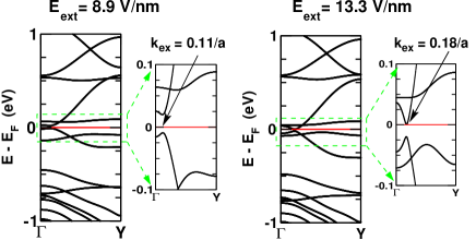
Figure 3 shows the evolution of the band-gap as a function of the external electric field for three selected nano-ribbons, respectively 10-ANR, 16-ANR and 24-ANR. In general we observe that the band-gap drops more rapidly with as the size of the -ANRs gets larger. Such a width dependence can be easily rationalized by assuming again little interaction between the two ribbon edges. In this case the potential difference between the edges necessary to close the gap is the same regardless of the ribbon size. If one now assumes that the potential drop inside the ribbon is approximately uniform (linear), we will conclude that larger ribbons necessitate smaller electric fields to sustain the same potential difference at the edges. As such the critical field, , decreases with the ribbon width and already for a 24-ANR it assumes a value around 4 V/nm.
Interestingly our calculated values for the critical field are quite similar to those obtained before for BN PRB_2008_77 and AlN,CPL_2009_469 despite the fact that the band-gaps in these materials are much larger. Such a fact however should not be surprising. In fact, the band-gap closure occurs because of the almost rigid shift of the edge-localized ribbon CB and VB when the field is applied. As such, the condition for gap closure is that the external field produces a potential difference, , at the nano-ribbon edges that matches the ribbon band-gap, , i.e. , where is the electron charge. Under the assumption of a linear potential drop (constant electric field) inside the ribbon, we obtain the relation , where is the ribbon dielectric constant along the transverse direction and is the ribbon width. The critical field for the gap closure then simply reads
| (1) |
where the second equality follows from the fact that the dielectric constant is approximately inversely proportional to the material band-gap. The equation (1) brings two important consequences. On the one hand, it tells us that the critical field for the gap closure is approximately materials independent. On the other hand, it establishes a decay of with the ribbon width.
Before the band-gap closes completely with increasing an interesting effect is observed in small sized ANRs (for example in 10-ANR), namely that the gap remains direct but it moves away from towards Y in the 1D Brillouin zone. This shift occurs simultaneously with the band-gap reduction and it is seen to become more pronounced as gets larger. Such an effect can be observed in Fig. 4 where the band-structure of the 10-ANR is plotted for two different values of the electric field. The band-gap shift away from appears because of the interaction between the two edges of the ribbon and can be explained with the help of a simple tight-binding model, which we develop next.
As already mentioned before, the CB and VB are extremely localized at the edges of the ANR, so that their dispersion is solely determined by the longitudinal dimension. Then we can model their electronic structure by considering a simple nearest-neighbour tight binding model for two linear chains (mimicking the two 1D edges). For the sake of simplicity, we take only orbitals in the model and the CB and VB are simply characterized by two different on-site energies, respectively and (L and R stand for left and right-hand side edge). This is of course a rather crude model, as both and orbitals are excluded. However, the band-gap closure and the formation of a magnetic moment both originate from the one-dimensional nature of the edge states and not from the details of their orbital composition. As such our simple model captures the essential features of this problem, while further details related to edge specific nature will be discussed later in the paper.
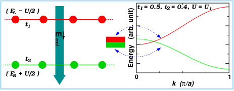
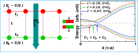
The two edges of a nanoribbon interact with each other in two possible ways. On the one hand, electrons can tunnel between the two edges with a probability given by the hopping integral . This is expected to decrease as the ribbon width becomes larger. On the other hand, upon the application of an external field, the bond-charges at the two ribbon edges will interact electrostatically. Such an interaction is taken into account by the dielectric response of the ribbon, which is described by the transverse component of the dielectric constant . As such, the potential difference between the ribbon edges, , is related to the external field simply as .
The 1D band-structures for the two edges are simply and , where and are the hopping integrals respectively of the left- and right-hand side chain, and is the 1D adimensional wave-vector (see Fig. 5). Let us assume that so that the left-hand side edge corresponds to the CB and the right-hand side one to the VB (the band-gap is at ). Let us also assume for the moment that there is no inter-chain interaction, i.e. that the hopping integral between the two chains vanishes, . Clearly, if there will be a gap between the CB and VB. The presence of an electric field simply shifts the on-site energy of the two bands. Thus the new on-site energies will be respectively and , with . This simple model then predicts that the band-gap will close for . For electric fields exceeding such value the ribbon will appear as a semi-metal, i.e. it will present coexisting electron and hole pockets at the point.
Let us now investigate the situation in which there is inter-chain interaction, i.e. between atoms localized on different chains (the atoms are assumed to be arranged on a square lattice). The new band-structure now takes the form
| (2) |
where the “” sign is for the CB and the “” one is for the VB. Clearly inter-chain hopping opens up a band-gap (of size 2) at the point along the -Y line, where the two bands would otherwise cross for (as shown in Fig. 5). It also indicates that, if the applied electric field increases further ( gets larger), the -point where the direct band-gap appears will shift towards Y, but the value of the band-gap itself will remain constant. It then follows that the band-gap closure occurs only if is reduced simultaneously as is increased (see the curve in Fig. 5 for ). This essentially suggests that the polarization of the edge state wave-functions under the influence of occurs in such a way as to reduce the effective interaction between the two edges of the ribbon. Notably the position in -space of the band-gap, , can be found by minimizing Eq. (2). This gives us , with .
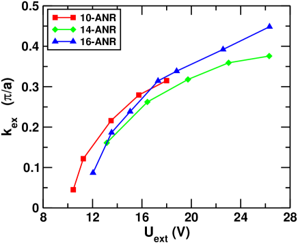
Such a qualitative picture agrees quite well with our DFT calculated , which is presented in Fig. 6 for small ANRs (). From the figure it is also worth noting, again in agreement with our simple model, that is practically independent from the ribbon size once the curve is plotted as a function of the external potential at the ribbon edges .
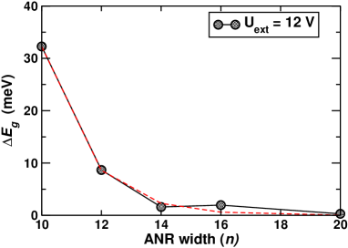
Finally, to conclude this section we make a number of addition observations, which further validate our model. Firstly we note that, as expected, the interaction between the ribbon’s edges gets stronger as the ribbon gets smaller. This means that the band repulsion at the band-gap along the -Y direction strengthens for small nano-ribbons. As a consequence the gap-closure occurs for relatively larger fields than those expected by a simple rigid band shift (see figure 3). Secondly, the position in -space of the gap immediately before its closure, , moves towards as the ribbon becomes wider. This essentially indicates that the inter-edge interaction, parameterized with , is reduced for large nano-ribbons. In order to prove such a fact in Fig. 7 we plot the band-gap as a function of the nano-ribbon size . This is calculated for an external electrostatic potential, Volt, sufficient to move the band-gap away from for all the ribbons investigated. In this situation the band-gap is a direct measure of the inter-edge hopping , 2. Notably the decay is rather severe indicating that already for relatively small ribbons () the inter-edge interaction becomes almost negligible.
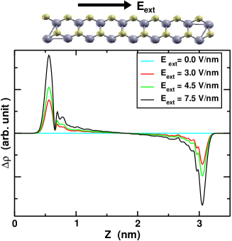
Finally we look at the charge density polarization induced in the ANRs by the external electric field. In figure 8 we plot the field-induced charge density distribution, , as a function of the position across the ribbon (-coordinate, see Fig. 1). Here is the difference between the charge density calculated in an applied field and that in no field, . Also note that all the densities are averaged over the plane. Notably there is charge accumulation at the positive potential edge and a corresponding depletion at the negative one. As such, a transverse field induces an electrical dipole across the ribbon, which effectively behaves as a capacitor.
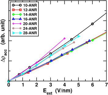
The accumulated charge can be calculated by simply integrating from one of the edge positions, , to the ribbon mid-point, , which is . This quantity is presented next in Fig. 9 as a function of and for different ANRs. Clearly is found to increase linearly with the field. This is the behaviour expected from a parallel plate capacitor. A second important observation, also consistent with viewing the ribbon as a parallel plate capacitor, is that the slope of the - curve is almost independent from the ribbon width. Minor variations can be attributed to our somehow arbitrary definition of the ribbon mid-point (this is defined in terms of the planar average of as the point where ) and to the fact that as the field increases and the ribbon band-gap is reduced, the dielectric constant changes.
In summary the evolution of the electronic properties of MoS2 armchair nano-ribbons as a function of an external transverse electric field can be understood in terms of the ribbon dielectric response, which is indeed consistent with that of a linear dielectric. These findings are rather general and can be easily transferred to other materials with different band-gaps. Next we examine the effects of stacking multiple MoS2 nano-ribbon layers.
Bi-layer and multi-layer MoS2-ANR
In 2D layered compounds the tiny inter-layer interaction is often sufficient to change drastically the electronic properties of the material. A prototypical example is graphene, where the weak - interaction is able to turn the linear band-dispersion into parabolic.BiLayer It becomes therefore natural to investigate how the results of the previous section get modified in multi-layered ribbons.
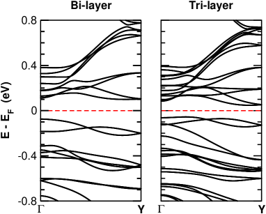
In order to keep the computational costs reasonable we consider here only the case of 8-ANRs, whose electronic band-structure in both a bi- and tri-layer form is presented in Fig. 10. As for bulk MoS2 also multi-layered nano-ribbons display an indirect band-gap, which is positioned along the -Y direction in the 1D Brillouin zone. We have extended our calculations to ANRs comprising up to five layers and, for comparison, to an infinite (periodic) nano-ribbon stacking. We notice that the band-gap turns indirect already for a bi-layer and then it remains indirect for any other structure. Furthermore, the band-gap decreases monotonically with increasing the number of layers. However, at variance with their parental 2D counterparts and similarly to the single-layer ribbons, also in multi-layered ANRs both the CB and the VB are localized over the ribbon edges. This fact is rather robust with respect to the interlayer-separation, in contrast to what happens to the fine details of the electronic structure of the infinite 2D multi-layers,vdWPRB so that the explicit inclusion of van der Waals interaction in the present context is not crucial. The localization of CB and VB at the edges means that, as in the single-layer case, also the multi-layers are sensitive to a transverse electric field.
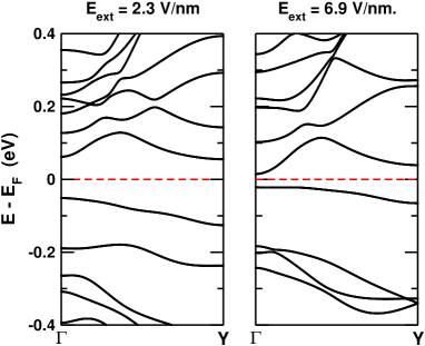
Such a sensitivity is examined next for the case of the 8-ANR bi-layer in Fig. 11. In general the response to is qualitatively similar to that of the single layers as it is determined by the electrostatic potential shift at the nano-ribbon edge. Thus as gets larger the energy shift of both the CB and VB localized at opposite edges results in a band-gap reduction. There is however a difference with respect to the single layer case, namely that the inter-layer interaction lifts the edge-band-degeneracy for . As a consequence the band-dispersion around the band-gap changes in a non-trivial way with the electric field. For instance for the case of the bi-layer 8-ANR first the CB minimum moves towards Y, thus strengthening the indirect nature of the gap and then, for larger fields, is reverts back to and eventually the band-gap becomes direct. This is an intriguing feature as it demonstrates that in multi-layers the nature of the band-gap can be manipulated by an external transverse field. As such one may expect, for instance, that the optical activity of such ribbons may be electrically modulated.
As a final observation we note that the critical fields for closing the gap in multi-layer ANRs are significantly smaller than those needed for the corresponding single-layer ones. Furthermore, for a fixed external field the band-gap is found to be inversely proportional to the number of layers, although a more precise dependence is difficult to establish. Such an inverse dependence is expected if the different layers in the multi-layer ribbon behave effectively like capacitors in parallel, although such an analogy cannot be pushed much further based on our DFT results.
Electrically driven magnetism
As the VB and the CB of a MoS2-ANR approach each other under the influence of a high DOS is generated at the Fermi level on the verge of the insulator to metal transition. Such high DOS originates from the Van Hove singularities at the band edges owing to the quasi-1D nature of the NRs. For the ANRs are non-magnetic semiconductors. Thus, for any fields smaller than the critical one for the band closure the system remains semi-conducting and no spin-polarized calculations are needed. However, at and beyond the onset of the metallic phase both spin polarized and non-spin polarized calculations have been performed in order to establish whether the ground state is stable against the formation of a finite magnetic moment. In general, we have found that at the critical electrical field, , where the bandgap closes there is a sufficiently high DOS at the (non-magnetic) Fermi level to drive the formation of a magnetic moment according to the Stoner criteria for ferromagnetism.
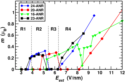
Figure 12 displays the evolution of the ribbon magnetic moment (per ribbon cell), , as a function of for three different ANRs. For example, one can clearly see that a 24-ANR becomes magnetic for V/nm, which is the critical field to close the gap completely. Such a transition from a diamagnetic to a magnetic ground state is driven by the Stoner criterion, which reads , where is the Stoner parameter (the exchange constant) and is the DOS at the Fermi level.Stoner ; Janak The Stoner parameter can be estimated from our DFT calculations, since the magnetic exchange splitting, , of the bands is given by ,PRB_1990_41_7028 where is the magnetic moment in units of the Bohr magneton . For instance, in the case of the 24-ANR at V/nm we find that eV and /unit cell, so that the estimated value of the Stoner parameter is eV and the required DOS at the Fermi level necessary to satisfy the Stoner instability condition is eV-1.
Also in Fig. 12 it can be observed that the critical field for the diamagnetic to magnetic transition corresponds exactly to , i.e. it coincides with the onset of metallicity (see Fig. 3). This is true for both the 20-ANR and the 24-ANR and for any larger ribbon. The situation however is different for the 16-ANR for which the magnetic transition occurs at a field smaller then . As noted previously, for small ribbons non-spin polarized calculations reveal that the inter-edge interaction creates a band anti-crossing, so that the critical field for the band-gap closure is larger than that needed for shifting rigidly the CB and the VB by the band-gap. Thus the metallic phase occurs at an larger than the one necessary to simply shifting the bands. In contrast, we find that once spin-polarization is allowed in the calculation, the semiconducting to metallic transition occurs virtually with the band edges of the VB and the CB touching at the point. This suggests that the exchange energy gained by spin-polarizing the system is sufficiently large to overcome the inter-edge interaction. Total energy calculations indeed confirm that the spin polarized ground state is energetically more favorable than the diamagnetic one. Hence, the 8-ANR undergoes a magnetic transition at a smaller that the Ec calculated from the LDA.
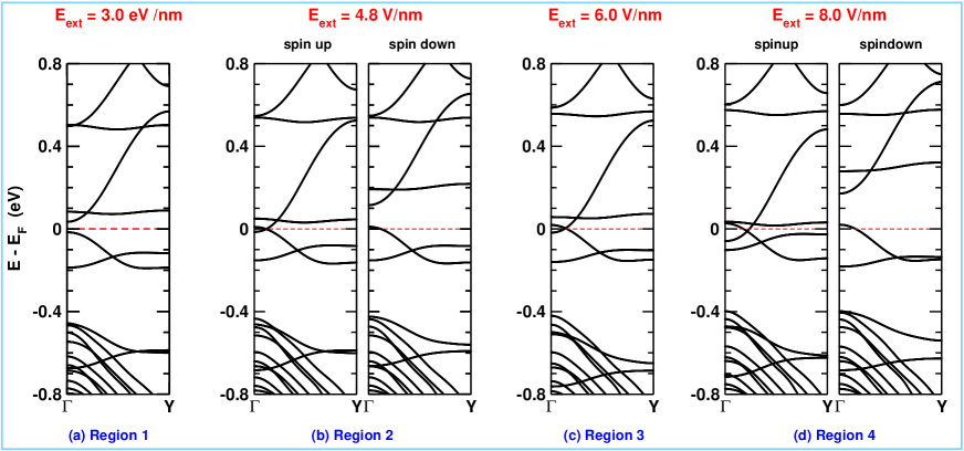
It is also interesting to look at what happens when the electric field is increased beyond the value needed for the first magnetic transition. Taking the case of the 24-ANR as an example we notice in Fig. 12 that there are different magnetic regions depending on . In particular we observe two diamagnetic regions (R1 and R3) and two magnetic ones (R2 and R4). R1 corresponds to the semi-conducting ground state of the ribbon and therefore it is non-magnetic. At the boundary between R1 and R2 the ribbon becomes metallic and the Stoner mechanism drives the electronic structure in a magnetic state. Further increase of , however, destroys the magnetic moment, which returns to zero in R3. Such a return of the diamagnetic phase can be understood by looking at Fig. 13, where we present the band-structure for the 24-ANR at four representative electric field strengths, corresponding respectively to the four regions. In R3 the field is strong enough to further shift the CB and VB in such a way that the Van Hove singularities are removed from . Now the electronic structure of the ribbon is that of a non-magnetic semi-metal with both an electron and a hole pocket at the Fermi level. As cuts now in a region where the bands have relatively large dispersion (small DOS) the Stoner criterion is no longer satisfied and the magnetic moment disappears. A further increase of the external field drives the system into R4, where now a new band from the CB manifold crosses the Fermi level and it is spin split by the Stoner exchange. The same mechanism works for the 20-ANR, while anomalies appear for the 16-ANR, again because of the more subtle inter-edge interaction.
Finally we wish to note that, as previously observed, the fact that the ribbon has inversion symmetry about its axis is irrelevant for the magnetic moment formation. This is demonstrated again in Fig. 12, where for completeness we report data for the 23-ANR as well. Clearly the 23-ANR and the 24-ANR display an almost identical pattern of magnetic moment formation with , except for minor details in the various critical positions for the on-set of the magnetism, which are mainly due to the slightly different confinement in the two structures.
Edge termination
We finally move to discuss the effects that the different edge terminations have on the onset of the electric field driven magnetism. Experimentally it was reported that MoS2 single layer clusters present a well defined edge structure.NatNanoT_2007_2 In particular it was shown that clusters above a certain critical size (about 1 nm) all display 100% rich Mo edges, i.e. the ones investigated so far throughout our work. This broadly agrees with earlier density functional theory calculations,Schweiger which however pointed out that alternative edge structures can form depending on the clusters growth environment. In particular it was reported that under hydrodesulfurization conditions S-terminated edges become more stable. It becomes then meaningful and intriguing to explore whether the results presented so far are robust against sulfurization of the edges.
Towards this goal we have repeated our calculations for the 24-ANR by replacing either one or both of the Mo edges with a different termination. In particular we have looked at three different cases, namely: 1) single 50% S-passivated edge, 2) single 100% S-passivated edge, 3) double 100% S-passivated edges. Furthermore for completeness, we have explored whether hydrogen passivation, alternative to the S one, produces any qualitative change.
In general we have found that, regardless of the termination, the valence and the conduction bands of the nanoribbon are always made of edge states, while their band dispersion and the actual bandgap do depend on the chemical nature of the edges. These two features suggest that the evolution of the bandgap in an external electric field should present similar qualitative features to those discussed previously, as the gap closure is simply dominated by the shift in the electrostatic potential at the ribbon edges. In contrast the formation of the magnetic moment, which depends on the band dispersion through the density of states and on the exchange interaction of the edge wave-function, may be sensitively affected by the details of the edge structure.
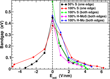
Fig. 14 shows the value of the bandgap as a function of the external electric field for all the terminations investigated. Note that, as some ribbons present different edges, the gap depends not only on the electric field intensity but also on its polarity. As such for these ribbons we plot results for both positive and negative . In general the figure confirms the intuitive picture presented above, i.e. for all the terminations studied we observe gap closure as a function of the electric field. The critical fields are also rather similar ranging between 4 V/nm (the same critical field for the case of two 100% Mo rich edges) to approximately 6 V/nm.
More intriguing is the influence of the edge termination on the formation of the magnetic moment. Here we find that some edges do not display any Stoner instability so that no magnetism is induced by the external field. This can be appreciated by looking at Fig. 15, where we plot the magnetic moment per cell as a function of .
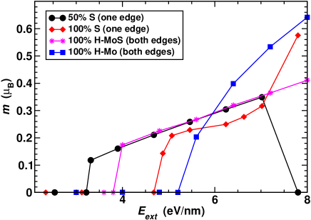
From the figure it appears that ANRs with either 50% or 100% S-rich edges can sustain a magnetic moment. However the figure refers to a 24-ANR in which only one edge has such termination, while the other still displays the Mo one. A closer look at the density of state reveals that the magnetic moment in this case forms only at the Mo edge, but not at the S-rich one. This brings the interesting consequence that the moment formation occurs only for one specific polarity of the electric field, which is the one necessary to bring the band associated to the Mo edge at the Fermi level. A second consequence is that when the sulfurization is at both edges no magnetic moment ever develops.
We then conclude that in S-rich edges the Stoner condition is not met, either because the density of states is not large enough or because the additional S contributes to reduce the Stoner parameter of the edge states. Interestingly H passivation does not seem to be detrimental to the magnetism. As suggested in Ref. [Terrones, ] we have investigated two types of passivations differing by whether the double passivation is only at the Mo site (this is labelled in Fig. 14 and Fig. 15 as “H-Mo”) or both at the Mo and the S ones (labelled as “H-MoS”). In this case the magnetic moment forms at both edges as soon as is large enough to close the gap, i.e. H-passivated edges behave identically to the unpassivated Mo ones.
Finally we conclude with some comments on the possible effects of disorder. Throughout this paper we have investigated only perfect edges, which is justified given the experimental observation of large clusters with perfect edges.NatNanoT_2007_2 However these clusters count at most approximately 20 sites per side and it is very unlikely that much larger nanoribbons can maintain such structural perfection. Defects and inhomogeneities of course break translational invariance so that the one-dimensional nature of the edge states will certainly be affected. One should then expect a general broadening of the edge-related bands with a consequent reduction of the average density of states. As such, because the magnitude of the density of states determines the Stoner condition, it is reasonable to expect that the formation of the magnetic moment will be rather sensitive to edge defects. In contrast the gap closure in an electric field should be more robust. This in fact depends only on the ability of creating a potential different between the edges, a feature that should not be affected too much by disorder.
CONCLUSIONS
In summary, we have investigated the ground state electronic structure and the electrical field response of MoS2 nano-ribbon structures. Our first principle calculations show that MoS2 ANRs are insulators with a direct band-gap regardless of the width. Importantly the band-gap in these systems is primarily determined by a pair of edge states and it may be tuned by applying an external transverse electric field. This can eventually drive a metal-insulator transition. It is important to note that the critical electric field for the transition can be reduced to a practical range with increasing ribbon width. Also it is interesting to remark that, as the dielectric constant is approximately proportional to the inverse of the band-gap, the critical fields for the gap closure are expected to be relatively materials independent.
The presence of localized edge states that can be moved to the Fermi level suggests that the system can be driven towards magnetic instability.
Our spin-polarized calculations show that this indeed happens and that at a certain critical electric field a diamagnetic to magnetic transition
occurs. This follows directly from the Stoner criterion as the Van Hove singularities associated to the edge states have a large density of
states. Intriguingly the magnetic phase can be further tuned by the external field and different alternating diamagnetic and magnetic regions
can be accessed.
METHODS
Electronic structure calculations are performed by using density functional theory (DFT) PRB_1964_136 ; PRA_1965_140 and the Ceperly-Alder parametrization PRL_1980_45 of the local spin density approximation (LSDA) to the exchange and correlation functional. In particular we employ the Siesta code.IOP_2002_14 A double- polarized Siesta_Basis numerical atomic orbital basis set for Mo and S is used together with the Troullier-Martins scheme for constructing norm-conserving pseudopotentials.PRB_1991_43 The pseudopotentials are generated by treating the following electronic states as valence: Mo: ; S: . An equivalent plane wave cutoff of 250 Ry is chosen for the real space grid and the Brillouin zone is sampled by using a Monkhorst-Pack grid. Periodic boundary conditions have been included and a vacuum layer of at least 15 Å is placed at the edges of the ribbon both in plane and out of plane in order to suppress the interaction between the ribbon periodic images. Conjugate gradient is used to obtain optimized geometries, where all the atoms in the unit cell are allowed to relax under the action of the external electric field until the forces on each atom are less than 0.03 eV/Å.
Acknowledgments
This work is supported by Science Foundation of Ireland (Grant No. 07/IN.1/I945). We thank Irish Centre for High End Computing (ICHEC) and Trinity Centre for High Performance Computing (TCHPC) for the computational resources provided.
References
- (1) Xia Y.; Yang P.; Sun Y.; Wu Y.; Mayers B.; Gates B.; Yin Y.; Kim F.; Yan H. One-Dimensional Nanostructures: Synthesis, Characterization, and Applications. Adv. Mat. 2003, 15, 353–389.
- (2) Wang X.; Li Y. Solution-Based Synthetic Strategies for 1-D Nanostructures. Inorg. Chem. 2006, 45, 7522–7534.
- (3) Cerrina F.; Marrian C. A Path to Nanolithography. MRS Bull. 1996, 21, 56–62.
- (4) Gibson J.M. Reading and Writing with Electron Beans. Phys. Today 1997, 50, 56–61.
- (5) Matsui S.; Ochiai Y. Focused Ion Beam Applications to Solid State Devices. Nanotech. 1996, 7, 247–258.
- (6) Levenson M.D.; Silverman P.J.; George R.; Wittekoek S.; Ware P.; Sparkes C.; Thompson L.; Bischoff P.; Dickinson A.; Shamaly J. Welcome to the DUV Revolution. Solid State Technol. 1995 38, 81–98.
- (7) Handbook of Nanostructured Materials and Nano-technology. Nalwa H.S., Eds.; Academic Press: New York, 2000.
- (8) Nakada K.; Fujita M.; Dresselhaus G.; Dresselhaus M.S. Edge State in Graphene Ribbons: Nanometer Size Effect and Edge Shape Dependence. Phys. Rev. B 1996, 54, 17954–17961.
- (9) Wakabayashi K.; Fujita M.; Ajiki H.; Sigrist M. Electronic and Magnetic Properties of Nanographite Ribbons. Phys. Rev. B 1999, 59, 8271–8282.
- (10) Han M.Y.; Özyilmaz B.; Zhang Y.; Kim P. Energy Band-Gap Engineering of Graphene Nanoribbons. Phys. Rev. Lett. 2007, 98, 206805.
- (11) Ding Y.; Wang Y.; Ni J. Electronic Structures of BC3 Nanoribbons. Appl. Phys. Lett. 2009, 94, 073111.
- (12) Luo X.; Yang J.; Liu H.; Wu X.; Wang Y.; Ma Y.; Wei S.-H.; Gong X.; Xiang H. Predicting Two-Dimensional Boron Carbon Compounds by the Global Optimization Method. J. Am. Chem. Soc. 2011, 133, 16285–16290.
- (13) Park C.-H.; Louie S.G. Energy Gaps and Stark Effect in Boron Nitride Nanoribbons. Nano Lett. 2008, 8, 2200–2203.
- (14) Barone V.; Peralta J.E. Magnetic Boron Nitride Nanoribbons with Tunable Electronic Properties. Nano Lett. 2008, 8, 2210–2214.
- (15) Erickson K.J.; Gibb A.L.; Sinitskii A.; Rousseas M.; Alem N.; Tour J.M.; Zettl A.K. Longitudinal Splitting of Boron Nitride Nanotubes for the Facile Synthesis of High Quality Boron Nitride Nanoribbons. Nano Lett. 2011, 11, 3221–3226.
- (16) Pan Z.W.; Dai Z.R.; Wang Z.L. Nanobelts of Semiconducting Oxides Science 2001, 291, 1947–1949.
- (17) Botello-Méndez A.R.; Martínez-Martínez M.T.; López-Urías F.; Terrones M.; Terrones H. Metallic Edges in Zinc Oxide Nanoribbons Chem. Phys. Lett. 2007, 448, 258–263.
- (18) Kou L.; Li C.; Zhang Z.; Guo W. Tuning Magnetism in Zigzag ZnO Nanoribbons by Transverse Electric Fields. ACS Nano 2010, 4, 2124–2128.
- (19) Shi W.; Peng H.; Wang N.; Li C.P.; Xu L.; Lee C.S.; Kalish R.; Lee S.-T. Free-standing Single Crystal Silicon Nanoribbons. J. Am. Chem. Soc. 2001, 123, 11095–11096.
- (20) Ding Y.; Ni J. Electronic Structures of Silicon Nanoribbons. Appl. Phys. Lett. 2009, 95, 083115.
- (21) Zheng F.; Zhou G.; Liu Z. Wu J.; Duan W.; Gu B.-L.; Zhang S.B. Half Metallicity along the Edge of Zigzag Boron Nitride Nanoribbons. Phys. Rev. B 2008, 78, 205415.
- (22) Wilson J.A.; Yoffe A.D. The Transition Metal Dichalcogenides Discussion and Interpretation of the Observed Optical, Electrical and Structural Properties. Adv. Phys. 1969, 18, 193–335.
- (23) Friend R.H.; Yoffe A.D. Electronic Properties of Intercalation Complexes of the Transition Metal Dichalcogenides. Adv. Phys. 1987, 36, 1–94.
- (24) Verble J.L.; Wietling T.J.; Reed P.R. Rigid-Layer Lattice Vibrations and Van der Waals Bonding in Hexagonal MoS2. Solid State Commun. 1972, 11, 941–944.
- (25) Novoselov K.S.; Jiang D.; Schedin F.; Booth T.J.; Khotkevich V.V.; Morozov S.V.; Geim A.K. Two-Dimensional Atomic Crystals. Proc. Nat. Acad. Sci. U.S.A. 2005, 102, 10451–10453.
- (26) Coleman J.N. et al. Two-Dimensional Nanosheets Produced by Liquid Exfoliation of Layered Materials. Science 2011, 331, 568–571.
- (27) Novoselov K.S.; Geim A.K.; Morozov S.V.; Jiang D.; Zhang Y.; DubonosS.V.; Grigorieva I.V.; Firsov A.A. Electric Field Effect in Atomically Thin Carbon Films. Science 2004, 306, 666–669.
- (28) Radisavljevic B.; Radenovic A.; Brivio J.; Giacometti V.; Kis A. Single-Layer MoS2 Transistors. Nature Nanotech. 2011, 6, 147–150.
- (29) Lauritsen J.V.; Kibsgaard J.; Helveg S.; Topsøe H.; Clausen B.S.; Lægsgaard E.; Besenbacher F. Size-Dependent Structure of MoS2 Nanocrystals. Nature Nanotech. 2007, 2, 53–58.
- (30) Lauritsen J.V.; Kibsgaard J.; Olesen G.H.; Moses P.G.; Hinnemann B.; Helveg S.; Nørskov J.K.; Clausen B.S.; Topsøe H.; Lægsgaard E.; Besenbacher F. Location and Coordination of Promoter Atoms in Co- and Ni-Promoted MoS2-Based Hydrotreating Catalysts. J. Catal. 2007, 249, 220–233.
- (31) Li T.; Galli G. Electronic Properties of MoS2 Nanoparticles. J. Phys. Chem. C 2007, 111, 16192–16196.
- (32) Son Y.-W.; Cohen M.L.; Louie S.G. Half-Metallic Graphene Nanoribbons. Nature (London) 2006, 444, 347–349.
- (33) Du A.J.; Zhu Z.H.; Chen Y.; Lu G.Q.; Smith S.C. First Principle Studies of Zigzag AlN Nanoribbon. Chem. Phys. Lett. 2009, 469, 183–185..
- (34) Iijima S. Helical Microtubules of Graphitic Carbon. Nature (London) 1991, 354, 56–58.
- (35) Hamada N.; Sawada S.; Oshiyama A. New One-Dimensional Conductors: Graphitic Microtubules Phys. Rev. Lett. 1992, 68, 1579–1782.
- (36) Li Y.; Zhou Z.; Zhang S.; Chen Z. MoS2 Nanoribbons: High Stability and Unusual Electronic and Magnetic Properties. J. Am. Chem. Soc. 2008, 130, 16739–16744.
- (37) Wang, Z. et al. Mixed Low-Dimensional Nanomaterial: 2D Ultranarrow MoS2 Inorganic Nanoribbons Encapsulated in Quasi-1D Carbon Nanotubes. J. Am. Chem. Soc. 2010, 132, 13840–13847.
- (38) Avetisyan A.A.; Partoens B.; Peeters F.M. Electric Field Tuning of the Band Gap in Graphene Multilayers. Phys. Rev. B 2009, 79, 035421.
- (39) Böker Th.; Severin R.; Müller A.; Janowitz C.; Manzke R.; Voess D.; Krüger P.; Mazur A.; Pollmann J. Band Structure of MoS2, MoSe2, and -MoTe2: Angle-Resolved Photoelectron Spectroscopy and Ab Initio Calculations. Phys. Rev. B 2001, 64, 235305.
- (40) Fives K.; McGovern I.T.; McGrath R.; Cimino R.; Hughes G.; McKinley A.; Thornton G. The Photoelectron Bandstructure of Molybdenum Disulphide J. Phys.: Condens. Matter 1992, 4, 5639–5646.
- (41) Kobayashi K.; Yamauchi J. Electronic Structure and Scanning-Tunneling-Microscopy Image of Molybdenum Dichalcogenide Surfaces. Phys. Rev. B 1995, 51, 17085–17095.
- (42) Helveg S.; Lauritsen J.V.; Lægsgaard E.; Stensgaard I.; Nørskov J.K.; Clausen B.S.; Topsøe H.; Besenbacher F. Atomic-Scale Structure of Single-Layer MoS2 Nanoclusters. Phys. Rev. Lett. 2000, 84, 951–954.
- (43) Splendiani A.; Sun L.; Zhang Y.; Li T.; Kim J.; Chim C.-Y.; Galli G.; Wang F. Emerging Photoluminescence in Monolayer MoS2. Nano Lett. 2010, 10, 1271–1275.
- (44) Mak K.F.; Lee C.; Hone J.; Shan J.; Heinz T.F. Atomically Thin MoS2: A New Direct-Gap Semiconductor. Phys. Rev. Lett. 2010, 105, 136805.
- (45) Han S.W. et al. Band-Gap Transition Induced by Interlayer Van der Waals Interaction in MoS2. Phys. Rev. B 2011, 84, 045409.
- (46) Hart C.F. Exact k-q Solution for a Bloch Electron in a Constant Electric Field. Phys. Rev. B 1988, 38, 2158–2161.
- (47) O’Keeffe J.; Wei C.Y.; Cho K.J. Bandstructure Modulation for Carbon Nanotubes in a Uniform Electric Field. Appl. Phys. Lett. 2002, 80, 676–678 (2002).
- (48) Son Y.-W.; Cohen M.L.; Louie S.G. Energy Gaps in Graphene Nanoribbons Phys. Rev. Lett. 2006, 97, 216803.
- (49) Zhang Z.; Guo W. Energy-Gap Modulation of BN Ribbons by Transverse Electric Fields: First-Principles Calculations Phys. Rev. B 2008, 77, 075403.
- (50) Novoselov K.S.; McCann E.; Morozov S.V.; Fal’ko V.I.; Katsnelson M.I.; Zeitler U.; Jiang D.; Schedin F.; Geim A.K. Unconventional Quantum Hall Effect and Berry’s Phase of 2 in Bilayer Graphene. Nature Physics 2006, 2, 177–180.
- (51) Ramasubramaniam, A.; Naveh , D; Towe E. Tunable Band Gaps in Bilayer Transition-Metal Dichalcogenides. Phys. Rev. B 2011, 84, 205325-1–205325-10.
- (52) Stoner E.C. Collective Electron Ferromagnetism. II. Energy and Specific Heat. Proc. R. Soc. London Ser. A 1939, 169, 339–371.
- (53) Janak J.F. Uniform Susceptibilities of Metallic Elements. Phys. Rev. B 1977, 16, 255–262.
- (54) Stollhoff G.; Oles A.M.; Heine V. Stoner Exchange Interaction in Transition Metals. Phys. Rev. B 1990, 41, 7028–7041.
- (55) Schweiger H.; Raybaud P.; Kresse G.; Toulhoat H. Shape and Edge Sites Modification of MoS2 Catalytic Nanopartciles Induced by Working Conditions: a Theoretical Study. J. Catal. 2002, 207, 76–87.
- (56) Botello-Méndez A.R.; López-Urás F.; Terrones M.; Terrones H. Metallic and Ferromagnetic Edges in Molybdenum Disul de Nanoribbons. Nanotech. 2009, 20, 325703.
- (57) Hohenberg P.; Kohn W. Inhomogeneous Electron Gas. Phys. Rev. 1964, 136, B864–B871.
- (58) Kohn W.; Sham L.J. Self-Consistent Equations Including Exchange and Correlation Effects. Phys. Rev. 1965, 140, A1133–A1138.
- (59) Ceperly D.M.; Alder B.J. Ground State of the Electron Gas by a Stochastic Method. Phys. Rev. Lett. 1980, 45, 566–569.
- (60) Soler J. M.; Artacho E.; Gale J. D.; García A.; Junquera J.; Ordejón P.; Sánchez-Portal D. The SIESTA Method for Ab Initio Order- Materials Simulation. J. Phys.: Condens. Matter 2002, 14, 2745–2779.
- (61) Junquera J.; Paz O.; Sánchez-Portal D.; Artacho E. Numerical Atomic Orbitals for Linear-Scaling Calculations. Phys. Rev. B 2001, 64, 235111.
- (62) Troullier N.; Martins J.L. Efficient Pseudopotentials for Plane-Wave Calculations Phys. Rev. B 1991 43,1993–2006.