Effects of disorder and contacts on transport through graphene nanoribbons
Abstract
We study the transport of charge carriers through finite graphene structures. The use of numerical exact kernel polynomial and Green function techniques allows us to treat actual sized samples beyond the Dirac-cone approximation. Particularly we investigate disordered nanoribbons, normal-conductor/graphene interfaces and normal-conductor/graphene/normal-conductor junctions with a focus on the behavior of the local density of states, single-particle spectral function, optical conductivity and conductance. We demonstrate that the contacts and bulk disorder will have a major impact on the electronic properties of graphene-based devices.
pacs:
73.63.-b, 73.40.-c, 72.10.-d, 72.15.RnI Introduction
During the last decade graphene and graphene based nanostructures have attracted a great amount of attention in regard to both fundamental research and application device engineering. Most of the unique electronic properties of graphene originate from the strictly two-dimensional arrangement of carbon atoms on a honeycomb lattice and the related gapless conical low-energy spectrum around the corners ( and points) of the hexagonal Brillouin zone. There bulk graphene supplies charge carriers that have sublattice and valley pseudospins, feature the pseudorelativistic dynamics of (massless) Dirac fermions and consequently possess a fixed chirality (helicity). These characteristics lead to many unusual and sometimes counterintuitive charge transport phenomena such as a finite “universal” dc conductivity at the neutrality point, Klein tunneling, or an anomalous quantum Hall effect; for a recent review see Ref. Castro Neto et al., 2009. Concerning the optical properties, within the Dirac cone approximation, only transitions across the Dirac point that are vertical in momentum space are allowed, leading to a frequency-independent absorption of undoped graphene.Yuan et al. (2011) For doped graphene the optical response is greatly reduced for frequencies smaller than twice the absolute value of the Fermi energy due to Pauli’s exclusion principle, while for larger frequencies it is roughly given by an universal ac conductivity.Scharf et al. (2013)
Recent breakthroughs in graphene fabrication and patterning facilitated the realization of graphene based electronics, plasmonics and optics. In particular graphene nanoribbons (GNRs) with varying widths down to a few nanometer and graphene quantum dots have been prepared and operated with field-effect transistor, filter, polarizer or electronic lens functionalities. The striking electronic properties of these GNR based nanostructures are strongly dependent on their geometry and edge shape.Gunlycke et al. (2007); Sevincli et al. (2008); Zhao and Guo (2009) GNRs with zigzag or armchair shaped edges develop specific band structures.Ezawa (2006, 2007) Thereby, for a realistic modeling of the GNR’s quasiparticle energies and band gaps, edge passivation, edge closure and edge bond relaxation have to be taken into account.Son et al. (2006); Zhao and Guo (2009); Kunstmann et al. (2011) In narrow armchair GNRs with hydrogen termination aromatic (Clar) sextets largely affect the band gap and consequently the transport properties.Wassmann et al. (2010) For hydrogen-terminated zigzag GNRs the spin polarization of edge states comes into play.Sevincli et al. (2008); Gunlycke et al. (2007); Wassmann et al. (2010) Moreover, as a matter of course, the enhanced screened Coulomb interaction gives rise to significant self-energy corrections for both zigzag and armchair GNRs.Yang et al. (2007) Lastly the leads (contacts) connecting the active graphene element to the electronic reservoirs play always an important role, just as the interfaces in graphene junctions and the substrate.
Regrettably transport through graphene and GNRs based devices will be strongly affected by disorder,Castro Neto et al. (2009); Mucciolo and Lewenkopf (2010) i.e., scattering potentials caused by intrinsic impurities, bulk defects induced by the substrate, ripples, edge roughness, adsorbent atoms at unsaturated dangling bonds at the boundary of the sample, and adatoms on graphene’s open surface. Disorder is known to be exceedingly efficient in suppressing the charge carrier’s mobility in low-dimensional systems, even to the point of Anderson localization. However graphene shows distinctive features in this respect too. First, only short-range impurities may cause intervalley scattering leading to Anderson localization.Anderson (1958) Second, due to the chirality of the charge carriers quantum interference may trigger even weak antilocalization.Tikhonenko et al. (2009) Third, charge carrier density fluctuations may break up the sample into electron-hole puddles; mesoscopic transport is then determined by activated hopping or leakage between the puddles. Recent observations of Coulomb diamondlike features in device conductance suggest that charge transport in GNRs occurs through quantum dots forming along the ribbon due to a disorder potential induced by charged impurities.Gallagher et al. (2010)
Experimentally important information about the transport and optical properties of (disordered) GNRs comes from scanning tunneling microscopy, angle resolved photoemission spectroscopy, (infrared) optical conductivity and conductance measurements, scanning probe spectroscopy, current flow and life time measurements.
Theoretically these quantities are best obtained by unbiased numerical approaches which enable—if many-body interaction effects can be neglected—the treatment of actual sized contacted GNRs with and without disorder beyond the simple continuum Dirac fermion description.
In this paper we use highly efficient Chebyshev expansion,Weiße and Fehske (2008) kernel polynomialWeiße et al. (2006) and Green functionDatta (1995) techniquesFUSH13 (2013) to analyze the electronic properties of GNRs with zigzag and armchair edges (Sec. II), as well as disordered normal-conductor(graphene)/GNR junctions (Sec. III). To this end, we calculate the local density of states, the single-particle spectral function, the optical conductivity and the conductance for different geometries. Special attention is paid to disorder effects. Studying the influence of disorder on the transport behavior of (contacted) GNRs a tight-binding approach is generally accepted to be a first reasonable starting point.Castro Neto et al. (2009); Xiong and Xiong (2007); Robinson et al. (2008); Martin and Blanter (2009); Bang and Chang (2010); Yuan et al. (2011); Cheraghchi (2011); Son et al. (2011); González-Santander et al. (2013) Then the Hamiltonian for this problem can be written as
| (1) |
where is a fermionic annihilation (creation) operator acting on lattice site of a honeycomb lattice with sites, denotes pairs of nearest neighbors and the site-dependent on-site potentials can take values appropriate for the system under consideration.
II Disordered Graphene Nanoribbons
II.1 Local Density of States
The local properties of a graphene sample with broken translational invariance are best reflected by the local density of states (LDOS),
| (2) |
where , and is a single-electron eigenstate of with energy . Experimentally the LDOS is directly probed by scanning tunneling microscopy.Niimi et al. (2009) Theoretically, can be determined to, de facto, arbitrary precision by the kernel polynomial method (KPM), which is based on the expansion of the rescaled Hamiltonian into a finite series of Chebyshev polynomials.Weiße et al. (2006); Weiße and Fehske (2008) Exploiting the local distribution approach,Alvermann and Fehske (2005, 2008) the distribution of the LDOS may be used to distinguish localized from extending states, e.g., in order to address the problem of Anderson localization in graphene.Schubert et al. (2010); Schubert and Fehske (2012)
II.1.1 Regular internal boundaries
In addition to the extraordinary bulk properties of graphene, finite graphene structures have very interesting surface (edge or boundary) states that do not exist in other systems. For example, the spectrum of GNRs depends on the nature of their edges: zigzag or armchair.Nakada et al. (1996); Brey and Fertig (2006); Ezawa (2006, 2007) The experimental ability to prepare zigzag edges selectively by an (anisotropic) crystallographic etching process was demonstrated quite recently.Oberhuber et al. (2013) A zigzag GNR [with periodic boundary conditions (PBC) along the direction] presents a band of zero-energy modes. This band is due to surface states living at and close to the graphene edges. In contrast, the density of states of armchair GNRs is gapped at . We note that zigzag GNRs with hydrogen passivation might also have a gapped band structure provided that edge magnetization exists,Son et al. (2006); Gunlycke et al. (2007) which is not very likely at least at room temperatures however.Kunstmann et al. (2011)
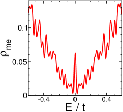
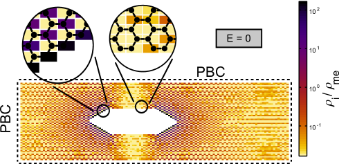
Localized states can also appear if a boundary inside the graphene material exists. This is demonstrated by Fig. 1 for a “regular” void, realized via infinite on-site potentials . The magnifications show that the internal boundaries are of zigzag and armchair types. The four zigzag boundaries give reason to a band of edge states that shows up by a strong peak in the averaged (mean) DOS, , at , see left panel. Note that for such GNRs with voids the localized states located at the sublattice with open bonds do not allow an analytical solution. The additional peaks in the mean DOS are remainders of the sequence of Van Hove singularities, appearing in finite GNRs due to their quasi one-dimensionality.Schubert et al. (2009)
II.1.2 Rough external boundaries
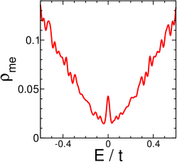
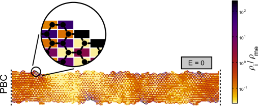
The fabrication procedure of GNRs usually does not yet allow us to control the boundary of a GNR with atomic precision. Hence the edges of GNRs are disordered as a rule on the atomic length scale, with the result that the transport properties might differ significantly from those of ideal GNRs.Martin and Blanter (2009); Fischetti and Narayanan (2011) To model a rough graphene boundary, we repeatedly remove edge sites (carbon atoms with only two nearest neighbors) from the GNR,Mucciolo et al. (2009) just by setting the corresponding with probability . If we create by chance “antenna” (carbon atoms with only one neighbor) or isolated atoms, these will be removed as well. Figure 2 gives the mean DOS and LDOS for such a GNR with rough edges. Starting from a GNR with ideal armchair edges along the direction, the typical sample depicted was obtained after 30 reiterations of the above described procedure. Both the mean DOS and LDOS signal the existence of localized edge states which arise because small zigzag regions are generated at the GNR boundary by the cropping process. The LDOS furthermore shows that—caused by the edge roughness—the sites in the bulk with weak (or even vanishing) amplitude of the wavefunction form a filamentary network. Simultaneously the Van Hove singularities are smeared out as an effect of disorder.
II.2 Momentum-resolved spectral function
The KPMWeiße et al. (2006); Weiße and Fehske (2008) can also be used to calculate spectral functions and dynamical correlation functions for disordered GNRs. The influence of disorder on the electronic properties of graphene and GNRs is of particular interest in the vicinity of the Dirac point. Angle resolved photoemission spectroscopy provides the most direct method to investigate the electronic band structure in this region.Bostwick et al. (2010) Quite recently also (small scale rotational) disorder effects have been probed by photoemission measurements for (epitaxial) graphene (on SiC(0001)).Walter et al. (2013)
Here we investigate GNRs with short-range Anderson disorder, ,Schubert et al. (2009) and determine the momentum-resolved single-particle spectral function at zero temperature (),
| (3) |
where (note that is not a Bloch eigenstate of infinite graphene due to its sublattice structure).
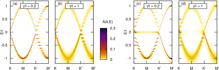
Figure 3 presents results for along paths following the Brillouin zone boundary thereby meeting the Dirac points and . The discreteness of the spectra in the vertical direction is a finite-size effect (due to the small in GNRs with sites), causing a sequence of quasi one-dimensional bands with Van Hove singularities. They primarily appear along the () direction for armchair (zigzag) GNRs. These finite-size signatures will be readily suppressed by disorder away from the Dirac points but persist near , even for relatively large values of [see panel (b)], indicating that the Dirac fermions are less affected by Anderson disorder. Most notably the almost dispersionsless band of edge states, appearing in zigzag GNRs along - for weak disorder [see panel (c)], is destroyed for strong disorder, where only a few localized edge states reside near the , points [see panel (d)].
II.3 Optical conductivity
We next analyze the optical response of disordered GNRs by calculating the so-called regular contribution to the real part of the optical conductivity
| (4) |
by our KPM scheme.Weiße et al. (2006) In Eq. (4), the current operator ( denotes the component of the position vector ) , the Fermi function , and with Å.
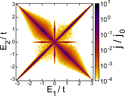
Valuable information about the transport properties can already be obtained from the temperature- and filling-independent current matrix-element density
| (5) |
Here the trace can be evaluated by a stochastic method using a small number—in our case ten—randomly chosen states for each sample.Skilling (1988); Weiße et al. (2006)
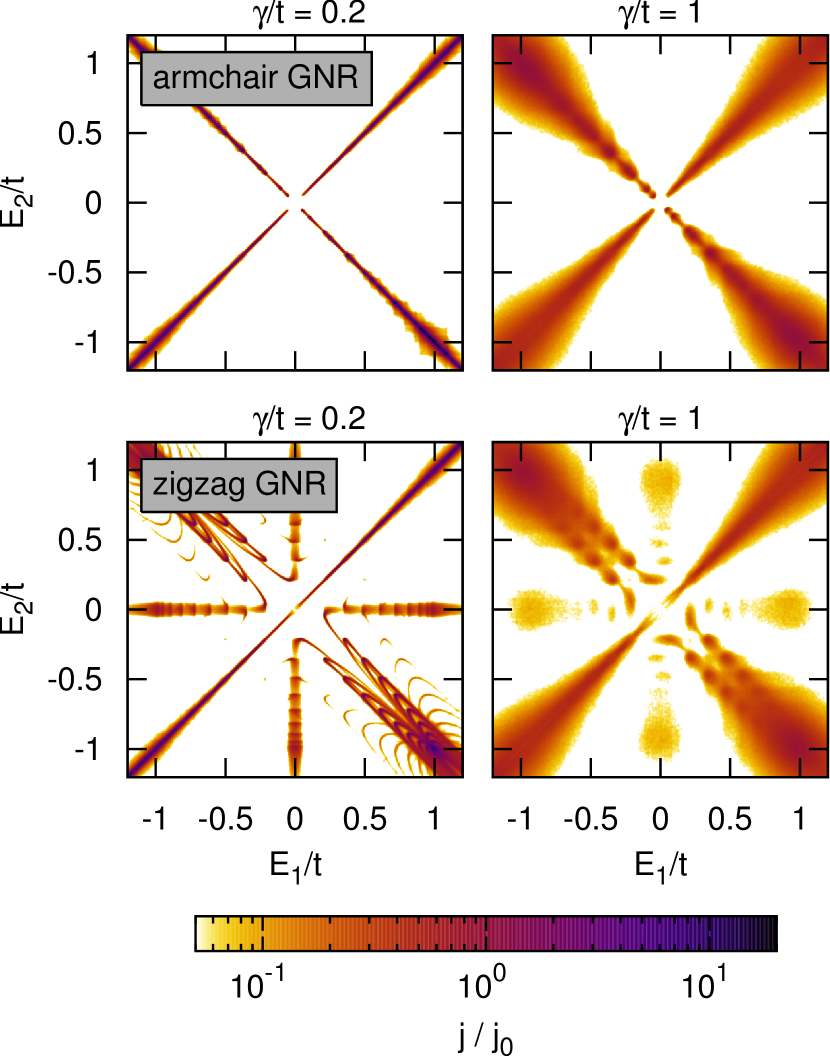
For graphene, the current matrix-element density exhibits finite spetral weight only on an “X”-shaped support in the - plane, where the line accounts for the dc conductivity (). The line , on the other hand, describes the ac optical response due to vertical - interband transitions (recall that and do not commute for the non-interacting graphene honeycomb lattice model). For GNRs boundary effects will strongly affect these signatures.
Figure 4 displays and for the zigzag case. First of all the spectral signature at widens out. Of higher significance, however, will be the additional “”-shaped absorption feature which can be attributed to optical transitions between edge and bulk states. The optical conductivity at fixed , according to the second line of Eq. (4), is given by an integral over , where the Fermi factors filter out contributions located in the second and fourth quadrant only. Furthermore, they suppress below , yielding a step feature. If compared to the optical response of bulk graphene, showing besides this step a single maximum at the DOS Van Hove singularity point only, the edge states in zigzag GNRs lead to a further step at and an additional local maximum at , see right panel. Clearly, for , we find a Drude peak at , i.e. at finite filling, whereas at the charge neutrality point ().
Figure 5 contrasts the current density for disordered armchair and zigzag GNRs for the same parameters as the spectral function was shown in Fig 3. In armchair GNRs the spectral weight is appreciable near the “X”-shaped support for the regular and weakly disorders cases. Near the origin disorder effects are almost negligible. At large a broading sets in that emanates from the point . This effect is also observed for zigzag GNRs but superimposed by the “” shaped absorption feature, which becomes broadened by the disorder as well. Since the zigzag GNR under consideration has a noticeable smaller width compared with that used in Fig. 4, finite-size effects influence the optical transitions in the vicinity of even for relatively strong disorder, particularly when .
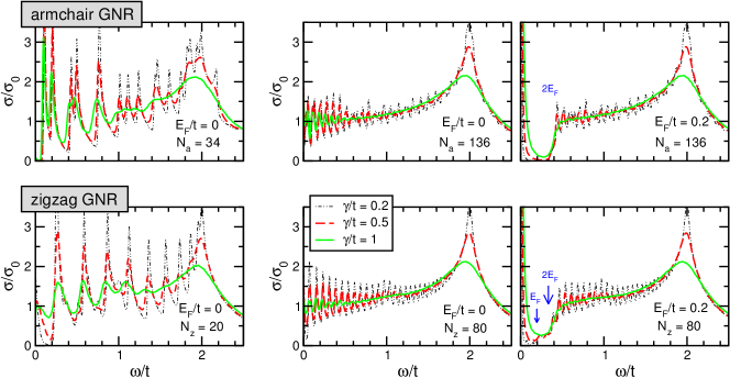
The resulting optical response of armchair and zigzag GNRs of different width is shown in Fig. 6 for different disorder strengths . Obviously the conductivity of narrow GNRs is dominated by Van Hove DOS effects. Naturally the corresponding maxima in weaken as the ribbon width increases, except the one at caused by the 2D graphene honeycomb lattice structure. The higher the optical frequency, the stronger these finite-size signatures will be reduced by Anderson disorder. Also the maximum at is suppressed. On the other hand, away from the charge neutrality point, disorder enhances the optical response in the region , because the (Pauli) blocking of states could be locally overcome. Furthermore, we find that the above mentioned fingerprints of edge states in zigzag GNRs survive the presence of disorder to a large extent.
To subsume, the combined LDOS, single-particle spectral function and optical conductivity results presented in this section give a largely consistent picture of how disorder affects the electronic and transport properties of isolated GNRs.
III Normal-conductor graphene junctions
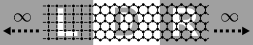
In a next step, we address the (linear) transport through disordered GNR in the lead-sample geometry most relevant for experiments. The ultimate electronic contacts are metallic or gated graphene. The coupling between graphene and the metallic electrodes can be realized by hybridization. In general it is extremely difficult to describe this coupling within ab initio approaches. Therefore simplified models have been proposed to describe normal-metal/graphene (NG) junctions.Blanter and Martin (2007); Robinson and Schomerus (2007); Do and Dollfus (2010); Zhang and Qin (2010); Zhang et al. (2012) We consider here only two-terminal contact systems, as schematized in Fig. 7. End-contacts, instead of side-contacted setups, might be justified when the nanostructure/electrode coupling is strong, which means good transparency of the interfaces and weak chemical bonding.Krompiewski (2012)
For small bias voltages, within the Landauer-Büttiker formalism, the phase-coherent conductance equals the transmission functionDatta (1995); Ferry and Goodnick (1997)
| (6) |
where the lead-system coupling matrices
| (7) |
contain the self-energies describing the contacts (L/R), and the Green function of the system (D) is
| (8) |
In case of a homogeneous ballistic conductor, simply counts the number of propagating modes. Each transport channel contributes to the conductance. For a zigzag GNR we have . then increases away from the charge neutrality point (for large almost straight proportional to ) and reaches its maximum at , before it falls off again and becomes zero at the edge of the spectrum . Modeling the metallic lead by a tight-binding square-lattice Hamiltonian with sites in direction, we find , , and as . The NG interface couples these modes to the propagating and evanescent modes in the graphene scattering region D.
III.1 Influence of contacts
Let us first consider zigzag (armchair) graphene interfaces connected to square-lattice-matched metallic leads by assuming that the lattice constant of the metal (). Furthermore, we fix () and hypothesize the same Fermi energy and transfer amplitude to exist in the metal respectively NG link. Then conductance shows the behavior displayed in Fig. 8 (armchair GNR with metal-to-zigzag-graphene interface) and Fig. 9 (zigzag GNR with metal to armchair-graphene interface). Most notably, close to the charge neutrality point, we observe in all cases an almost linear dependency of the conductance on the absolute value of the Fermi energy . The slope in the - () and -type () regime in general differs however. Armchair GNRs with zigzag interface match better to metallic quantum wires because there exists an equivalent mode selection.Schomerus (2007) Obviously the slope near does not much depend on ’. We nevertheless observe a significant overall reduction of and a strong asymmetry for away from the Dirac point, if there are dangling bonds on the GNR side of the interface. The same holds for zigzag GNRs with armchair interfaces but here the latter effect leads to a stronger reduction of in the -type regime.
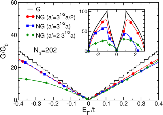
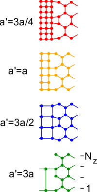
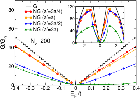
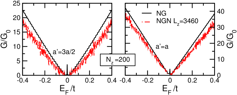
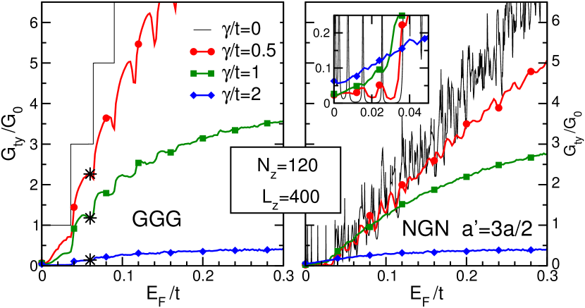
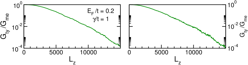
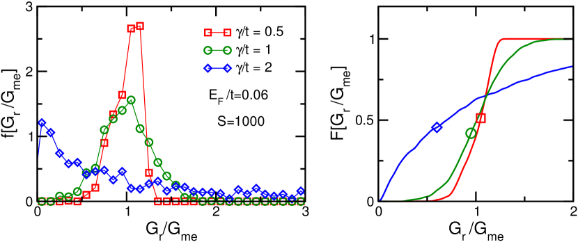
Figure 10 shows the conductance for a clean normal-metal /graphene/normal-metal (NGN) junction, where a zigzag GNR with a length-to-width aspect ratio of ten was sandwiched between two metallic leads. Since the intervening GNR acts as a scattering center, is smaller than for a both-sided semi-infinite NG junction. The scattering gives rise to a strongly fluctuating . The average value of is higher for the interface with because there are more transport channels (modes) available on the metal sides of the contacts.
III.2 Effects of impurity scattering
Finally we investigate disordered GNRs encased by ordered graphene or metal leads. Defects and impurities are inevitable in graphene based devices. Anderson disorder—with on-site potentials drawn from a box distribution—can be used to model the effects of short-range impurity scattering by local imperfections. Quite generally the treatment of disordered systems requires the study of distributions of physical quantities, making the application of statistical methods necessary.Abou-Chacra et al. (1973); Alvermann and Fehske (2005) In particular this applies to the investigation of subtle disorder phenomena, such as Anderson localization.Schubert et al. (2010) To characterize the transport through disordered graphene junctions the conductance should be analyzed in this manner.
Calculating the conductance for realizations of an end-contacted disordered (zigzag) GNR (see Fig. 7), the mean sample-averaged conductance strongly fluctuates if gets small. This particularly happens near the Dirac point, for large disorder and long GNRs, i.e., when Anderson localization induced states appear. Then the conductance, just as the LDOS,Schubert et al. (2010) exhibits a log-normal (rather than a normal) distribution, whose maximum is strongly finite-size dependent. If the probability distribution becomes even singular at . To reflect such behavior the typical conductance,
| (9) |
is more appropriate than (inter alia because it puts sufficient weight on small values of ).
Figure 11 gives the variation of with the (Fermi) energy for different disorder strengths. Here the left (right) panel shows a GGG (NGN) junction. Without disorder, the GGG realizes a homogeneous GNR and we observe the step-growth of as increases, when more and more transport channels become available. For NGN junctions, a fluctuating results (see the discussion of Fig. 10). With disorder, for GGG junctions, an overall reduction of takes place. Thereby the steps will be blurred. At very large , even for finite , indicating Anderson localization. Already for , the transport behavior of GGG and NGN junctions is essentially the same. Disorder suppresses the inherent conductance fluctuations of clean NGN junctions, thereby it might even enhance the conductance at small (see inset). Interestingly, for weak disorder, we observe a “negative differential conductance” in the vicinity of the steps. This effect is more pronounced at larger energies and can be ascribed to the small curvature (flatness) of the bands if leaving/entering an old/new transport channel, making these states very susceptible to disorder. The lower panels impressively demonstrate that as increases at fixed for (any) , whereas stays finite. For , Anderson localization occurs not before .
We now determine the probability distribution of the conductance, , by accumulating the values of , calculated at a given energy for random samples of fixed size, within a histogram. Out of it the integrated distribution
| (10) |
can be obtained. The results are shown in Fig. 12. For weak disorder, when the finite disordered GNR junctions is transmissible, the probability distribution of the conductance is rather symmetric and peaked close to its mean value. In this regime the distribution is almost unaffected upon increasing the size of the GNR (not shown). For strong disorder, the distribution of is asymmetric and markedly depends on . Although most of the weight now is concentrated close to zero, the distribution extends to very large values of . That is, the mean value is much large than the most probable value and does not give any valuable information about the transport behavior. While for weakly disordered GGG junctions the more or less uniform conductances lead to a steep rise of at , for strong disorder a very gradual increase is observed. Disordered NGN junctions show the same tendencies.
IV Conclusions
By exact numerics we have studied the electronic and transport properties of finite (but actual sized) graphene based structures and demonstrated that the geometry of the sample and in particular edges, voids, contacts, and disorder strongly affects the local density of states, the single-particle spectrum, the ac conductivity and the conductance, probed scanning tunneling microscopy, angle resolved photoemission spectroscopy, optical response and two-terminal transport measurements, respectively.
We showed that localized edge states dominate the mean density of states (DOS) of graphene nanoribbons (GNRs)—which feature voids or rough surfaces—near the charge neutrality point. In the latter case, sites in the edge region having vanishing amplitude entail a filamentary network of the local DOS in the bulk. For disordered GNRs, both the averaged single-particle spectral function and optical conductivity indicate that disorder tends to suppress the finite-size effects caused by the geometry of the nanoribbon. The states near the , point are robust against disorder to the greatest possible extent. This does not apply to the band of localized edge states.
The conductance of edge-contacted GNR sensitively depends on the lead-GNR matching conditions. In this respect armchair GNRs enable a somewhat better current injection. Dangling bonds on the GNR side of the interface substantially reduce the conductance. The typical conductance of disordered GNRs sandwiched between graphene leads in a junction setup exhibits a negative differential conductivity whenever new transport channels become available by increasing the Fermi energy. This accentuates the efficiency of Anderson localization effects at the band edges of electronically low-dimensional systems. For GNR junctions, the conductance distribution function manifests a precursor of the transition from a current-carrying to an (Anderson disorder induced) insulating behavior, which is expected to takes place when the size of the disordered active graphene region becomes infinite.
Finally, let us emphasize once more that all these results were obtained within the limits of a non-interacting nearest-neighbor tight-binding model, plus on-site disorder and contacts. Thereby more subtle electronic structure and many-body effects were neglected. From a quantum chemical point of view the -electron distribution and geometric aspects, such as bond length and hexagon area alternations at and near the edges, for sure should be more seriously taken into account for narrow (aromatic) armchair GNRs,Wassmann et al. (2010) maybe by an effective third nearest neighbor hopping.Zhao and Guo (2009) While such couplings will significantly influence the band gap—and hence the transport properties of clean GNRs—Anderson localization, if present owing to bulk disorder, should be less affected. Coulomb interaction effects are particularly important for zigzag GNRs, where spin polarised edge states have been predicted.Yang et al. (2007) An equal-footing treatment of disorder and Coulomb correlations in low-dimensional many-particle systems has turned out to be extremely difficult. Modeling possible magnetic properties/functionalities of (disordered) zigzag GNRs by an ad hoc spin-polarizing field might help to keep the problem tractable.Gunlycke et al. (2007) These will be interesting directions for continuative work.
Acknowledgments
This work was supported by the Deutsche Forschungsgemeinschaft through the priority programmes 1459 ‘Graphene’ and 1648 ‘Software for Exascale Computing’. Part of this work was performed at the Center for Integrated Nanotechnologies at Los Alamos National Laboratory (DOE Contract DE-AC52-06NA25396).
References
- Castro Neto et al. (2009) A. H. Castro Neto, F. Guinea, N. M. R. Peres, K. S. Novoselov, and A. K. Geim, Rev. Mod. Phys. 81, 109 (2009).
- Yuan et al. (2011) S. Yuan, R. Roldán, H. De Raedt, and M. I. Katsnelson, Phys. Rev. B 84, 195418 (2011).
- Scharf et al. (2013) B. Scharf, V. Perebeinos, J. Fabian, and P. Avouris, Phys. Rev. B 87, 035414 (2013).
- Gunlycke et al. (2007) D. Gunlycke, D. A. Areshkin, J. Li, J. W. Mintmire, and C. T. White, Nano Lett. 7, 3608 (2007).
- Sevincli et al. (2008) H. Sevincli, M. Topsakal, and S. Ciraci, Phys. Rev. B 78, 245402 (2008).
- Zhao and Guo (2009) P. Zhao and J. Guo, J. Appl. Phys 105, 034503 (2009).
- Ezawa (2006) M. Ezawa, Phys. Rev. B 73, 045432 (2006).
- Ezawa (2007) M. Ezawa, phys. stat. sol. (c) 4, 489 (2007).
- Son et al. (2006) Y.-W. Son, M. L. Cohen, and S. G. Louie, Phys. Rev. Lett. 97, 216803 (2006).
- Kunstmann et al. (2011) J. Kunstmann, C. Özdogan, A. Quandt, and H. Fehske, Phys. Rev. B 83, 045414 (2011).
- Wassmann et al. (2010) T. Wassmann, A. P. Seitsonen, A. M. Saitta, M. Lazzeri, and F. Mauri, J. Am. Chem. Soc. 132, 3443 (2010).
- Yang et al. (2007) L. Yang, C.-H.Park, Y.-W. Son, M. L. Cohen, and S. G. Louie, Phys. Rev. Lett. 99, 186801 (2007).
- Mucciolo and Lewenkopf (2010) E. R. Mucciolo and C. H. Lewenkopf, J. Phys. Condens. Matter 22, 273201 (2010).
- Anderson (1958) P. W. Anderson, Phys. Rev. 109, 1492 (1958).
- Tikhonenko et al. (2009) F. V. Tikhonenko, A. A. Kozikov, A. K. Savchenko, and R. V. Gorbachev, Phys. Rev. Lett. 103, 226801 (2009).
- Gallagher et al. (2010) P. Gallagher, K. Todd, and D. Goldhaber-Gordon, Phys. Rev. B 81, 115409 (2010).
- Weiße and Fehske (2008) A. Weiße and H. Fehske, Lecture Notes in Physics 739, 545 (2008).
- Weiße et al. (2006) A. Weiße, G. Wellein, A. Alvermann, and H. Fehske, Rev. Mod. Phys. 78, 275 (2006).
- Datta (1995) S. Datta, Electronic Transport in Mesoscopic Systems (Cambridge University Press, Cambridge, 1995).
- FUSH13 (2013) Note that these techniques quite recently have been proven to be extremely efficent in calculating—on graphics processing units—electron transport in grahene samples; see Z. Fan, A. Uppstu, T. Siro, and A. Harju, arXiv:1307.0288.
- Xiong and Xiong (2007) S.-J. Xiong and Y. Xiong, Phys. Rev. B 76, 214204 (2007).
- Robinson et al. (2008) J. P. Robinson, H. Schomerus, L. Oroszlány, and V. I. Fal’ko, Phys. Rev. Lett. 101, 196803 (2008).
- Martin and Blanter (2009) I. Martin and Y. M. Blanter, Phys. Rev. B 79, 235132 (2009).
- Bang and Chang (2010) J. Bang and K. J. Chang, Phys. Rev. B 81, 193412 (2010).
- Cheraghchi (2011) H. Cheraghchi, Phys. Sr. 84, 015702 (2011).
- Son et al. (2011) Y. Son, H. Song, and S. Feng, J. Phys. Condens. Matter 23, 205501 (2011).
- González-Santander et al. (2013) K. L. Lee, B. Grémaud, C. Miniatura, and D. Delande, Phys. Rev. B 87, 144202 (2013); C. González-Santander, F. Domínguez-Adame, M. Hilke, and R. A. Römer EPL 104, 17012 (2013);
- Schubert et al. (2010) G. Schubert, J. Schleede, K. Byczuk, H. Fehske, and D. Vollhardt, Phys. Rev. B 81, 155106 (2010).
- Niimi et al. (2009) Y. Niimi, H. Kambara, and H. Fukuyama, Phys. Rev. Lett. 102, 026803 (2009).
- Alvermann and Fehske (2005) A. Alvermann and H. Fehske, Eur. Phys. J. B 48, 295 (2005).
- Alvermann and Fehske (2008) A. Alvermann and H. Fehske, Lecture Notes in Physics 739, 505 (2008).
- Schubert and Fehske (2012) G. Schubert and H. Fehske, Phys. Rev. Lett. 108, 066402 (2012).
- Nakada et al. (1996) K. Nakada, M. Fujita, G. Dresselhaus, and M. S. Dresselhaus, Phys. Rev. B 54, 17954 (1996).
- Brey and Fertig (2006) L. Brey and H. Fertig, Phys. Rev. B 73, 195408 (2006).
- Oberhuber et al. (2013) F. Oberhuber, S. Blien, S. H. F. Yaghobian, T. Korn, C. Schüller, C. Strunk, D. Weiss, and J. Eroms, Appl. Phys. Lett. 103, 143111 (2013).
- Schubert et al. (2009) G. Schubert, J. Schleede, and H. Fehske, Phys. Rev. B 79, 235116 (2009).
- Fischetti and Narayanan (2011) M. V. Fischetti and S. Narayanan, J. Appl. Phys 110, 083713 (2011).
- Mucciolo et al. (2009) E. R. Mucciolo, A. H. Castro Neto, and C. H. Lewenkopf, Phys. Rev. B 79, 075407 (2009).
- Bostwick et al. (2010) A. Bostwick, F. Speck, T. Seyller, K. Horn, M. Polini, R. Asgari, A. H. MacDonald, and E. Rotenberg, Science 328, 999 (2010).
- Walter et al. (2013) A. L. Walter, A. Bostwick, F. Speck, M. Ostler, K. S. Kim, Y. J. Chang, L. Moreschini, D. Innocenti, T. Seyller, K. Horn, et al., New J. Phys. 15, 023019 (2013).
- Skilling (1988) J. Skilling, in Maximum Entropy and Bayesian Methods, edited by J. Skilling (Kluwer, Dordrecht, 1988), Fundamental Theories of Physics, pp. 455–466.
- Blanter and Martin (2007) Y. M. Blanter and I. Martin, Phys. Rev. B 76, 155433 (2007).
- Robinson and Schomerus (2007) J. P. Robinson and H. Schomerus, Phys. Rev. B 76, 115430 (2007).
- Do and Dollfus (2010) V. N. Do and P. Dollfus, J. Phys. Condens. Matter 22, 425301 (20110).
- Zhang and Qin (2010) G. P. Zhang and Z. J. Qin, Phys. Lett. A 374, 4140 (2010).
- Zhang et al. (2012) G. P. Zhang, Y. Y. Z. M. Gao, N. Liu, Z. J. Qin, and M. H. Shangguan, J. Phys. Condens. Matter 24, 235303 (2012).
- Krompiewski (2012) S. Krompiewski, Nanotechnology 23, 135203 (2012).
- Ferry and Goodnick (1997) D. K. Ferry and S. M. Goodnick, Transport in Nanostructures (Cambridge University Press, 1997).
- Schomerus (2007) H. Schomerus, Phys. Rev. B 76, 045433 (2007).
- Abou-Chacra et al. (1973) R. Abou-Chacra, D. J. Thouless, and P. W. Anderson, J. Phys. C 6, 1734 (1973).