Nonlocal transport and heating in superconductors under dual-bias conditions
Abstract
We report on an experimental and theoretical study of nonlocal transport in superconductor hybrid structures, where two normal-metal leads are attached to a central superconducting wire. As a function of voltage bias applied to both normal-metal electrodes, we find surprisingly large nonlocal conductance signals, almost of the same magnitude as the local conductance. We demonstrate that these signals are the result of strong heating of the superconducting wire, and that under symmetric bias conditions, heating mimics the effect of Cooper pair splitting.
pacs:
74.25.F-, 74.40.Gh, 74.78.NaI Introduction
In hybrid proximity structures consisting of a normal metal and a superconductor (NS) electrons can be converted into Cooper pairs. Depending on the electron energy this conversion is provided by different physical mechanisms. Electrons with overgap energies may easily penetrate from a normal metal deep into a superconductor causing electron-hole branch imbalance Tinkham and Clarke (1972); *tinkham1972b which relaxes at macroscopic distances from the NS interface. In contrast, electrons with subgap energies penetrate into a superconductor by the mechanism of Andreev reflection (AR).Andreev (1964) In this case an electron propagating in a normal metal may enter a superconductor only at a rather short distance (of order of the superconducting coherence length ) forming a Cooper pair together with another electron taken from the same normal metal. At sufficiently low energies this Andreev reflection mechanism is responsible for dissipative charge transfer across NS interfaces.Blonder et al. (1982)
In multi-terminal hybrid proximity structures, such as NSN systems, the physics of low energy electron transport becomes much richer as it also includes coherent non-local effects. Provided the superconductor size (i.e. the distance between two NS interfaces) is comparable with (or smaller than) , two extra charge transfer mechanisms gain importance. One of them is the so-called elastic cotunneling (EC), i.e. direct transfer of subgap electrons between two N-metals through a superconductor. Another mechanism is crossed (or non-local) Andreev reflection Byers and Flatté (1995); Deutscher and Feinberg (2000) (CAR). In contrast to local AR, here a Cooper pair is formed by two electrons penetrating into a superconductor from two different N-terminals. This mechanism essentially influences non-local charge transport in hybrid NSN systems. Furthermore, employing the phenomenon of CAR one can provide a direct experimental realization of entanglement between electrons in different normal terminals. In other words, three-terminal NSN devices can effectively act as Cooper pair splitters.Lesovik et al. (2001); Recher et al. (2001); Hofstetter et al. (2009); Herrmann et al. (2010)
Both experimentalBeckmann et al. (2004); Beckmann and Löhneysen (2007); Russo et al. (2005); Cadden-Zimansky and Chandrasekhar (2006); Kleine et al. (2009); Almog et al. (2009); Kleine et al. (2010); Brauer et al. (2010); Wei and Chandrasekhar (2010); Kaviraj et al. (2011) and theoreticalFalci et al. (2001); Bignon et al. (2004); Brinkman and Golubov (2006); Morten et al. (2006); Kalenkov and Zaikin (2007a); Duhot and Melin (2007); Golubev and Zaikin (2007); Levy Yeyati et al. (2007); Kalenkov and Zaikin (2007b, 2008); Golubev and Zaikin (2009); Golubev et al. (2009); Bergeret and Levy Yeyati (2009); Golubev and Zaikin (2010); Freyn et al. (2010) (see also further references therein) investigations of dissipative electron transport and non-local shot noise in three-terminal NSN structures revealed a rich variety of non-trivial features. For instance, in the tunneling limit and at EC and CAR contributions to non-local conductance exactly cancel each other,Falci et al. (2001) thus leaving no possibility to experimentally test the effect of CAR in transport experiments in this limit. Splitting the contributions of EC and CAR becomes possible either at higher interface transmissions Kalenkov and Zaikin (2007a, b) or by applying an external ac field Golubev and Zaikin (2009) or, else, by studying non-local shot noise.Bignon et al. (2004); Wei and Chandrasekhar (2010); Kaviraj et al. (2011); Golubev and Zaikin (2010)
Further interesting features emerge in the presence of disorder. In this case an interplay between CAR, quantum interference of electrons and non-local charge imbalance dominates the behavior of diffusive NSN systems Golubev et al. (2009) and, for instance, may yield strong enhancement of non-local conductance in the low energy limit. The effect of disorder needs to be taken into account for a quantitative interpretation of the experiments.Cadden-Zimansky and Chandrasekhar (2006); Kleine et al. (2009); Almog et al. (2009)
Non-trivial physics also emerges from an interplay between CAR and Coulomb interaction. E.g., interactions lift the exact cancellation of EC and CAR contributions to the non-local differential conductance already in the lowest order in tunneling.Levy Yeyati et al. (2007) This conductance is predicted to have an S-like shape and can turn negative at non-zero bias.Golubev and Zaikin (2010) Furthermore, one can prove Golubev and Zaikin (2010) that there exists a fundamental relation between Coulomb effects and non-local shot noise in NSN structures which can be directly tested in future experiments.
In this work we will explore yet another physical effect which – along with the above mentioned ones – can essentially influence the behavior of three-terminal NSN proximity structures. Namely, we will demonstrate – both experimentally and theoretically – that non-local transport properties of such structures can be strongly affected (or even dominated) by heating. It is important to emphasize that under certain conditions heating can mimic both the effect of CAR and Cooper pair splitting. Thus, it is in general mandatory to account for heating effects while analyzing non-local phenomena in multi-terminal proximity structures.
The structure of our paper is as follows. In Sec. II we describe our NSN samples as well as the key aspects of our experiments. In Sec. III we present our experimental results demonstrating an importance of heating effects for non-local electron transport in the structures under consideration. Theoretical model aimed to quantitatively explain our experimental observations is worked out in Sec. IV. In Sec. V we make use of this model demonstrating a good agreement between theory and experiment without involving any fit parameters. Technical details of our derivation of the Coulomb correction to the non-local conductance are displayed in Appendix.
II Samples and Experiment
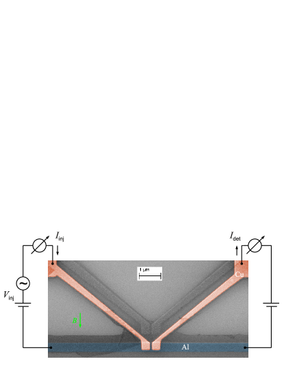
Our samples consist of a central superconducting wire, with several copper wires attached by tunnel junctions of normal-state conductance . The junctions are connected to the reservoirs by long normal-metal wires, which introduce a series resistance to create an Ohmic enviroment for the junctions. Figure 1 shows a false-color scanning electron microscopy image of one of the samples as well as a scheme of the measurement setup. The samples were fabricated by standard e-beam lithography and shadow evaporation techniques. In a first step, the superconducting aluminum wire of thickness nm was created. The aluminum wire was oxydized in situ to form a thin but pinhole-free tunnel barrier by exposing it to about Pa of pure oxygen for a few minutes. After the oxidation, copper of thickness nm was evaporated under a different angle to form the tunnel junctions. We investigated samples with two closely-spaced tunnel junctions as shown in Fig. 1, as well as one sample with six junctions to investigate the dependence of non-local transport on the contact distance (not shown). An overview of the sample parameters is given in Table 1.
All measurements were performed in a dilution refrigerator at temperatures down to mK. A magnetic field could be applied in the substrate plane perpendicular to the aluminum wire, as indicated in Fig. 1. A voltage consisting of a dc bias and a low-frequency ac excitation was applied to one tunnel contact, called injector, and the ac part of the resulting current was measured by standard lock-in techniques to obtain the local conductance . Simultaneously, the ac current through the second contact, held at fixed bias voltage , was measured to determine the nonlocal conductance .
Our key experimental results obtained in this way are outlined in the next section.
| Sample | junctions | (mS) | () | (nm) | (m) |
|---|---|---|---|---|---|
| A | 2 | 15 | 15 | ||
| B | 2 | 30 | 4.8 | ||
| C | 6 | 30 | 3 |
III Experimental results
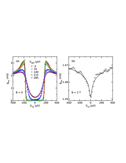
Figure 2(a) shows the local conductance of a junction of sample A as a function of injector bias for different detector bias at low temperature in the superconducting state. The data exhibit a well-defined energy gap and coherence peaks for , and an increased broadening for . In Figure 2(b), we also show the conductance at high magnetic field in the normal state. Here, a dip due dynamical Coulomb blockade is observed.
In order to fit the local conductance, we model the density of states in the superconductor including a phenomenological life-time broadening parameter (the so-called Dynes parameter Dynes et al. (1978)),
| (1) |
where is the quasiparticle energy and is the gap. The current through the tunnel junction is then given by
| (2) |
where is the voltage across the junction and is the Fermi function. For the samples with long copper wire, the series resistance is of similar magnitude as the junction resistance , and we cannot neglect the voltage drop across . The actual voltage across the junction is therefore , and we solve the implicit equation
| (3) |
for to fit the data. We thus have , , , and the temperature as fit parameters. We denote the temperature from these fits by , since it actually describes the smearing of the Fermi distribution in the normal metal. While and describe a similar broadening of the conductance features, we found that both had to be adjusted to give a good fit of the data. Fits to this model are shown as lines in Fig. 2(a). We proceeded by first fitting a trace at large detector bias, and then kept and fixed for all other fits. The high field data are fit with the standard model of dynamical Coulomb blockadeDevoret et al. (1990); Schön and Zaikin (1990); Ingold and Nazarov (1992), shown as a line in Fig. 2(b). For the latter fit, we kept the junction conductance fixed to its value in the superconducting state, and fit the series resistance as well as the effective impedance of the electromagnetic enviroment. The fact that in the normal state is larger than in the superconducting state reflects that the resistance of the aluminum wire now also appears in series with the junction. On the other hand, indicates that only a fraction of the series resistance actually affects dynamical Coulomb blockade, which probes the environment at high frequencies . A similar fit for sample B with the shorter Cu wire yields .
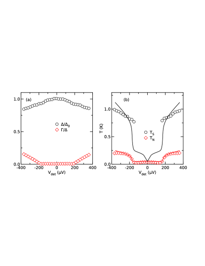
The parameters extracted from the fits in the superconducting state are shown in Fig. 3 as a function of detector bias . Figure 3(a) shows the gap normalized to its value at zero bias, as well as the normalized life-time broadening parameter . decreases by about 15 % with increasing bias, whereas remains about zero for , and sharply increases as soon as the bias exceeds the gap. The effective temperature behaves in a similar way as , as seen in Fig. 3(b). It remains close to the bath temperature below the gap, and then quickly increases to . To estimate the effective temperature of the quasiparticles in the superconductor, we have inverted the BCS temperature dependence of the gap to relate the decrease of as a function of bias to an increase of . Since is almost flat at low temperatures, the result of this inversion is not very reliable for small deviations of from . We therefore only plot the resulting for large bias in Fig. 3(b). As can be seen, . This results is reasonable since the electrons in the normal metal are heated indirectly by the quasiparticles in the superconductor.
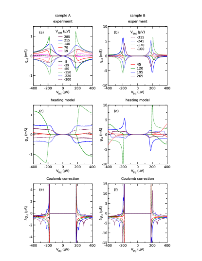
Figure 4 shows the nonlocal conductance for samples A and B. For (nearly) zero detector bias, we observe a signal of a few ten . A signal of this magnitude is expected due to charge imbalance, as described in detail in a previous publication.Hübler et al. (2010) The signal due to charge imbalance is an even function of injector bias, see Ref. Hübler et al., 2012. For finite detector bias, we observe two peaks in the nonlocal conductance. These exceed the charge imbalance signal by orders of magnitude, and are odd functions of both injector and detector bias. The peaks are relatively sharp and initially increase for . For , the peaks broaden and decrease considerably, much like the coherence peaks in the local conductance shown in Figure 2(a). The nonlocal conductance is negative if the sign of the injector and detector bias is the same, and positive otherwise. Symmetric bias conditions are the typical operating point for Cooper-pair splitter devices. Under these conditions, we observe negative nonlocal conductance, the same as one would find for crossed Andreev reflection.
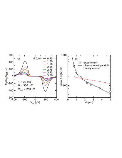
Finally, in Fig. 5(a) we show the dependence of the nonlocal conductance on contact distance for a fixed detector bias measured on sample C. The peaks described previously decrease slowly upon increasing , with little change in the overall shape. The maximum conductance is plotted on a semi-logarithmic scale as a function of in Fig. 5(b). The decay can be fit by the sum of two exponentials, with relaxation lengths and . The slow decay over a scale of several microns is compatible with nonequilibrium quasiparticle transport.
IV Non-local conductance and heating: Theoretical model
The behavior of the non-local conductance presented in Figs. 4 and 5 qualitatively resembles that in the presence of Coulomb effects Golubev and Zaikin (2010). On the other hand, our data demonstrate that - at least at sufficiently high voltages – heating effects are essential and, hence, should also be taken into account. The task at hand is to formulate a theoretical model which would adequately describe our system in the presence of both Coulomb interactions and heating effects.
In order to construct a complete theory of non-equilibrium heat transport in proximity structures it is in general necessary to employ the Keldysh technique and to work out a solution of inhomogeneous Usadel equations Belzig et al. (1999), see, e.g., Ref. Virtanen and Heikkil, 2007 for a review. The corresponding analysis turns out to be rather involved. For instance, substantial technical complications are due to the fact that in our problem the superconducting gap may acquire a significant coordinate dependence induced both by the proximity effect and by an inhomogeneous temperature profile inside the wire. Yet another complication has to do with the presence of electron-electron scattering, which leads to an effective equilibration of the quasiparticle distribution function at a certain length scale.
In order to proceed, below we will employ a simple model of non-local charge and heat transport through the structure depicted in Fig. 1. Within this model we will ignore the proximity effect assuming the resistances of the tunnel junctions to be sufficiently high. Then the coordinate dependence of may become important only at sufficiently strong overheating, i.e. provided the heat transport properties of a superconductor already resemble those of a normal metal. Our model does take into account the coordinate dependence of , but disregards Andreev reflection of quasiparticles associated with it. Therefore we expect it to be more accurate at relatively small overheating (low bias) and less accurate, but still qualitatively correct, at strong overheating (high bias). Within our model we will also assume that the electron-electron energy relaxation length is the shortest length scale in our problem and that the electron distribution function coincides with the Fermi function with the local electron temperature. The latter may deviate from the temperature of the phonon subsystem, which we assume to be the same as the base temperature of the cryostat. In order to justify the above assumption one can make use simple theoretical estimates of the electron-electron relaxation length at high energies and/or just quote earlier experiments with normal wires Pothier et al. (1997), in which this length – under the conditions similar to ours – was found to be of the order of or shorter than 1 m. This length scale is significantly shorter than the length of normal wires in our setup. We expect similar values of the relaxation length for strongly excited quasiparticles in aluminum, which give the main contribution to the signal at high bias. Thus the same arguments may be applied to the superconducting wire as well. As we will demonstrate, our simple model rather accurately describes the properties of the system under consideration.
Under the conditions outlined above the current through the detector junction can be expressed in the form
| (4) | |||||
Here are the voltage drops across the detector and injector junctions respectively. They are related to the potentials and (see Fig. 1) as follows
| (5) | |||||
| (6) |
where and are the resistances of the normal wires attached, respectively, to the detector and injector junctions. The voltage actually coincides with the voltage already introduced in Eq. (2).
The current of the detector (4) is the sum of four contributions. The first one, , is the standard tunneling current between normal and superconducting wires defined in Eq. (2). The minus sign in front of this contribution is due to the adopted sign convention, see Fig. 1. The second and the third contributions arise from the charge imbalance (CI) induced by non-equilibrium quasiparticles injected into the superconducting wire respectively through the detector junction and the injector,
| (8) |
and, finally, the fourth term, , is the Coulomb interaction correction Golubev and Zaikin (2010) derived in Appendix.
In the above expressions we introduced the following parameters: and are the left and right normal state resistances of the segments of the superconducting wire between the corresponding junctions and the bulk leads, and are the quasiparticle distribution functions respectively in the normal lead attached to the detector junction with temperature and in the superconductor with the local temperature , is the normal state value of the non-local conductance unaffected by Coulomb interaction.
According to Eqs. (4) and (6) the non-local conductance of the system reads
| (9) | |||||
This formula expresses as a function of the voltages and . In order to re-formulate it in terms of experimentally accessible voltages and , Eq. (9) should be employed in combination with Eqs. (5), (6).
The non-local conductance (9) contains two types of derivatives. The derivatives and remain finite even in equilibrium when the sample is well cooled and the temperature values in all electrodes do not depend on the bias voltages. The terms containing the derivatives over temperature account for the heating effect. It turns out that these terms give the dominant contribution to the non-local conductance in our samples.
As compared to the above terms, the Coulomb correction to the non-local conductance remains small and can be disregarded for the structures under consideration. In order to see that, let us set and choose . In this case the derivative may be expressed in a relatively simple form (see Appendix for details)
| (10) |
where we defined the high voltage cutoff determined by the inversed effective time of our system and introduced the dimensionless conductance of the electromagnetic environment “seen” by the detector. For our samples, we typically have . Thus, the Coulomb correction remains small except, perhaps, an immediate vicinity of the gap voltage , see Fig. 4e-f. This observation allows us to ignore the Coulomb interaction correction in our further consideration.
Our next step is to find the dependence of the temperatures , on the bias voltages and . For this purpose it will be necessary to solve the corresponding heat transport equations.
Let us first consider the normal lead attached to the detector. We will approximately treat it as a thin quasi-one-dimensional wire. The equation describing the heat transport along the wire reads
| (11) |
where we defined the coordinate along the wire and assumed that the detector junction is located at . The quantity denotes the heat power extracted from the normal wire or, equivalently, the cooling power of a detector wire. This quantity is given by the integral Giazotto et al. (2006)
| (12) |
which remains positive at and and turns negative in the high bias regime , . The first term in the right hand side of Eq. (11) describes the heat current from the electron subsystem into the phonon one, the material parameter characterizes the electron-phonon coupling strength, and stands for the cross sectional area of the detector normal wire. The second term in Eq. (11) describes the Joule heating of the wire by the current, and the last term is the heat current flowing along the wire and leaking into the outer bulk electrode. According to the Wiedemann - Franz law this heat current is proportional to the conductivity of the normal wire . Thus, Eq. (11) implies that the power generated in the biased detector junction is partially dissipated in the phonon subsystem and partially carried away along the wire.
Finally, Eq. (11) should be supplemented by the boundary conditions
| (13) |
where is the length of the detector normal wire. Here we assumed that at the wire is coupled to a bulk metallic lead kept at the base temperature . The heat transport in the normal wire attached to the injector is described by Eq. (11) with interchanged indices.
In order to fit our data, we numerically solved the heat balance equation (11). For the parameters of our samples we verified that the term responsible for electron-phonon interactions may be omitted provided the wire is short enough, i.e. , where
| (14) |
is the electron-phonon relaxation length. For the copper wire one has Giazotto et al. (2006) nW/m3K5. Combining this value with with the conductivity of our copper leads, , we find m at mK and m at K. Thus, the electron-phonon relaxation length indeed exceeds the length of the normal wire in both our samples in the whole range of temperatures relevant for our experiment.
Hence, we can safely omit the electron-phonon term from the differential equation (11). With this in mind one can easily integrate this equation reducing it to the algebraic one
| (15) |
where is the resistance of the detector normal wire. Similarly, for the injector normal wire one finds
| (16) |
We now turn to the heat transport equation in the superconducting wire. In this case the heat current from quasiparticles to phonons is in general defined by a rather complicated double integral. Here we will disregard the corresponding term in our heat transport equation from the very beginning assuming that overheating of our superconducting wire remains not too strong. This approximation requires that the superconducting wire length is smaller than the electron-phonon relaxation length in the superconductor , i.e.
| (17) |
where and are the conductivity and the electron-phonon coupling parameter in the normal state of the superconductor. We find that for our samples the condition (17) is satisfied in the range of voltages , but may be not fulfilled at higher voltages.
In order to further simplify our model we also assume that the detector and injector junctions are located close enough to each other, meaning that the temperature values on their superconducting sides are the same, i.e. . Under these conditions we can write the heat transport equation in the form
| (18) |
Here we assumed that both junctions are in the vicinity of the point , introduced the temperature of the superconductors at the point , , the heat current flowing to the direction and the heat current flowing in the opposite direction . The combination is the total heat power injected into the superconductor by both tunnel junctions. It is given by the sum of the Joule heating by both junctions, , and the total cooling power of both normal wires, . The boundary conditions for Eqs. (18) read
| (19) |
where and are the lengths of the wire segments on both sides of the junctions.
Next, is the quasiparticle heat current in the superconductor in presence of the temperature gradient. It reads
| (20) |
where is the cross sectional area of the superconducting wire and the heat conductivity of the superconductor is defined asBardeen et al. (1959)
| (21) |
Eq. (18) can be integrated in exactly the same way as Eq. (11). As a result, we arrive at the following algebraic equation
| (22) | |||||
where the function is defined as
and denotes the standard BCS temperature dependence of the superconducting gap.
Equations (15), (16) and (22) constitute a complete system which allows one to determine the temperatures , and as functions of the bias voltages. This system of equations was resolved numerically by iterations. The corresponding results are compared to the experiments in Figs. 3 and 4 and discussed below in the next section.
V Discussion and conclusions
The dependence of temperature on the bias voltage at for the parameters of the sample A predicted by the heating model is compared to the experimental data in Figs. 4(b). In agreement with the experiment one observes that the superconducting wire is overheated stronger than the normal wire, in particular at low bias values. This effect can easily be understood since in this regime the heat conductivity of the superconductor (21) is exponentially suppressed by the factor . Note that in our numerical simulations the broadening parameter was set equal to zero in the whole range of bias voltages. Enhanced smearing of the curves encountered at high bias voltages results from additional heating of the wires by the injector junction.
Our main results are depicted in Figs. 4(c) and (d), where the predicted nonlocal conductances of the samples A and B are plotted. We observe that our model not only qualitatively captures the behavior of as a function of the bias voltages and but also correctly predicts the magnitude of the non-local conductance. It is also important to stress that a good agreement between theory and experiment was achieved with no fit parameters as all resistances and other parameters were measured independently. Hence, we conclude that strong non-local response observed in our samples at not very small bias voltages is indeed due to the effect of heating.
Note that the model prediction for the dependence of the non-local signal on the distance between the junctions turns out to be not very accurate, see Fig. 5b. We speculate that the main cause for this discrepancy might be the effect of a finite electron-electron relaxation length which was considered short in our calculation. In any case, in order to quantitatively reproduce the two scale decay of the signal observed in our experiment it appears necessary to further refine the model employed in our theoretical analysis.
In Figs. 4(e) and (f), we also show the Coulomb correction predicted by eq. (10). Here, we have used the maximum of the charge imbalance signal measured at as , and the environmental resistance obtained from fitting the local Coulomb dip in the normal state. As can be seen, the Coulomb correction is qualitatively similar to the measured data, but too small by about three orders of magnitude.
Thermoelectric effects caused by the combination of a thermal gradient and a supercurrent have been observed in the 1970s.Clarke et al. (1979); Pethick and Smith (1979) These might also contribute to the nonlocal effects reported here. For aluminum, the magnitude of the nonlocal voltage due to these effects was found experimentally Heidel and Garland (1981) to be
| (24) |
For our experiment, we can estimate this contribution by assuming that the entire current, which is initially injected as quasiparticle current, is eventually converted to supercurrent. This yields an upper limit of the supercurrent density , where is the cross-section area of the aluminum wire. Since the quasiparticle temperature is increased by about over the bath temperature, and the observed effects decay on the length scale of a few microns, we can further estimate . For comparison with our nonlocal conductance experiment, we express eq. (24) in terms of injector voltage and detector current and obtain
| (25) |
This is orders of magnitude smaller than the observed effects. Also, in our experiment the driving force of the thermal gradient is heating due to the injector bias. The heating power, and therefore , is an even function of bias. The nonlocal conductance for this mechanism should also be even in bias according to eq. (25). We conclude that both by symmetry and order of magnitude the observed effects are not caused by charge imbalance in the presence of supercurrents and thermal gradients.
In summary, we demonstrated that heating can play a major role dominating the non-local properties of three-terminal hybrid proximity structures at not very small bias voltages. In simple terms this effect can be understood as follows. Increasing the bias voltage in the injector one effectively heats the superconductor which, in turn, yields the temperature increase in the detector wire. As a result, the detector current changes thus providing the non-local response. It turns out that in our samples this simple mechanism prevails – at least at substantial bias voltages – over more standard charge transfer mechanisms, such as charge imbalance or crossed Andreev reflection. Quite generally, the heating strength is controlled by the ratio between the wire resistances and those of the tunnel junctions. Heating effects are negligible provided this ratio is small, i.e. the junctions are more resistive than the wires. On the other hand, in the opposite limit of highly resistive wires heating gains importance and essentially influences the system behavior.
In particular, in a typical beam-splitter setup with equal bias across both junctions, increasing the current in one branch will lead to an increase in the other branch as well. This mimics Cooper pair splitting in multi-terminal proximity devices, and an adequate analysis of the experimental data is needed in order to avoid possible misinterpretations. Our theoretical model provides a proper tool for such analysis.
Finally, we would like to point out that even at rather small voltages heating effects in our structures can be non-negligible and should be treated on equal footing with, e.g., the effects of electron-electron interactions. This subject, however, requires a separate consideration which goes beyond the simple analysis presented here.
Acknowledgements
This work was partially supported by the Deutsche Forschungsgemeinschaft within the Center for Functional Nanostructures and by RFBR grant No. 12-02-00520-a.
Appendix A Coulomb correction to the current
The Coulomb correction to the current can be derived from the theory of environmental Coulomb blockade Ingold and Nazarov (1992). For simplicity, we first consider a single detector tunnel junction between normal and superconducting bulk leads. In this case the theoryIngold and Nazarov (1992) predicts the current in the form
| (26) |
where
| (27) |
is the probability to emit a photon with energy to the electromagnetic environment of the junction defined in terms of the phase correlation function
| (28) | |||||
Here is the impedance of the environment ”seen” by the detector tunnel junction. Here we will choose it in the form
| (29) |
where is an effective Ohmic shunt of the detector junction and is a (short) charge relaxation time depending on the effective junction capacitance . With a reasonable accuracy one can identify the shunt resistance with the resistance of the normal wire attached to the detector junction , i.e. .
Here we are mostly interested in the non-local contribution to the detector current. It can be derived in the same way as the main contribution to the current (26) repeating the procedure outlined, e.g., in the review Ingold and Nazarov (1992).
As a first step one assigns a phase factor (inj or det) to the tunneling amplitudes of the junctions treating the phases as quantum operators. This phase is related to the voltage fluctuations across the junctions, . Next, one performs the standard perturbative expansion of the current in powers of the tunneling Hamiltonians of the two junctions to the lowest non-vanishing order . Subsequent averaging over the phase fluctuations results in the product of the two functions . Leaving out further technical details, we go over to the final result which reads
| (30) |
Bearing in mind the property of the Fermi function , it is straightforward to check that in the non-interacting limit, where , the correction (30) reduces to the charge imbalance correction defined in the Eq. (8).
References
- Tinkham and Clarke (1972) M. Tinkham and J. Clarke, Phys. Rev. Lett. 28, 1366 (1972).
- Tinkham (1972) M. Tinkham, Phys. Rev. B 6, 1747 (1972).
- Andreev (1964) A. F. Andreev, Zh. Eksp. Teor. Fiz. 46, 1823 (1964) [Sov. Phys. JETP 19, 1228 (1964)].
- Blonder et al. (1982) G. E. Blonder, M. Tinkham, and T. M. Klapwijk, Phys. Rev. B 25, 4515 (1982).
- Byers and Flatté (1995) J. M. Byers and M. E. Flatté, Phys. Rev. Lett. 74, 306 (1995).
- Deutscher and Feinberg (2000) G. Deutscher and D. Feinberg, Appl. Phys. Lett. 76, 487 (2000).
- Lesovik et al. (2001) G. Lesovik, T. Martin, and G. Blatter, Eur. Phys. J. B 24, 287 (2001).
- Recher et al. (2001) P. Recher, E. V. Sukhorukov, and D. Loss, Phys. Rev. B 63, 165314 (2001).
- Hofstetter et al. (2009) L. Hofstetter, S. Csonka, J. Nygård, and C. Schönenberger, Nature 461, 960 (2009).
- Herrmann et al. (2010) L. G. Herrmann, F. Portier, P. Roche, A. Levy Yeyati, T. Kontos, and C. Strunk, Phys. Rev. Lett. 104, 026801 (2010).
- Beckmann et al. (2004) D. Beckmann, H. B. Weber, and H. v. Löhneysen, Phys. Rev. Lett. 93, 197003 (2004).
- Beckmann and Löhneysen (2007) D. Beckmann and H. v. Löhneysen, Appl. Phys. A 89, 603 (2007).
- Russo et al. (2005) S. Russo, M. Kroug, T. M. Klapwijk, and A. F. Morpurgo, Phys. Rev. Lett. 95, 027002 (2005).
- Cadden-Zimansky and Chandrasekhar (2006) P. Cadden-Zimansky and V. Chandrasekhar, Phys. Rev. Lett. 97, 237003 (2006).
- Kleine et al. (2009) A. Kleine, A. Baumgartner, J. Trbovic, and C. Schönenberger, Europhys. Lett. 87, 27011 (2009).
- Almog et al. (2009) B. Almog, S. Hacohen-Gourgy, A. Tsukernik, and G. Deutscher, Phys. Rev. B 80, 220512 (2009).
- Kleine et al. (2010) A. Kleine, A. Baumgartner, J. Trbovic, D. S. Golubev, A. D. Zaikin, and C. Schönenberger, Nanotechnology 21, 274002 (2010).
- Brauer et al. (2010) J. Brauer, F. Hübler, M. Smetanin, D. Beckmann, and H. v. Löhneysen, Phys. Rev. B 81, 024515 (2010).
- Wei and Chandrasekhar (2010) J. Wei and V. Chandrasekhar, Nature Physics 6, 494 (2010).
- Kaviraj et al. (2011) B. Kaviraj, O. Coupiac, H. Courtois, and F. Lefloch, Phys. Rev. Lett. 107, 077005 (2011).
- Falci et al. (2001) G. Falci, D. Feinberg, and F. W. J. Hekking, Europhys. Lett. 54, 255 (2001).
- Bignon et al. (2004) G. Bignon, M. Houzet, F. Pistolesi, and F. W. J. Hekking, Europhys. Lett. 67, 110 (2004).
- Brinkman and Golubov (2006) A. Brinkman and A. A. Golubov, Phys. Rev. B 74, 214512 (2006).
- Morten et al. (2006) J. P. Morten, A. Brataas, and W. Belzig, Phys. Rev. B 74, 214510 (2006).
- Kalenkov and Zaikin (2007a) M. S. Kalenkov and A. D. Zaikin, Phys. Rev. B 75, 172503 (2007a).
- Duhot and Melin (2007) S. Duhot and R. Melin, Phys. Rev. B 75, 184531 (2007).
- Golubev and Zaikin (2007) D. S. Golubev and A. D. Zaikin, Phys. Rev. B 76, 184510 (2007).
- Levy Yeyati et al. (2007) A. Levy Yeyati, F. S. Bergeret, A. Martín-Rodero, and T. M. Klapwijk, Nature Physics 3, 455 (2007).
- Kalenkov and Zaikin (2007b) M. S. Kalenkov and A. D. Zaikin, Phys. Rev. B 76, 224506 (2007b).
- Kalenkov and Zaikin (2008) M. Kalenkov and A. Zaikin, JETP Lett. 87, 140 (2008).
- Golubev and Zaikin (2009) D. S. Golubev and A. D. Zaikin, EPL 86, 37009 (2009).
- Golubev et al. (2009) D. S. Golubev, M. S. Kalenkov, and A. D. Zaikin, Phys. Rev. Lett. 103, 067006 (2009).
- Bergeret and Levy Yeyati (2009) F. S. Bergeret and A. Levy Yeyati, Phys. Rev. B 80, 174508 (2009).
- Golubev and Zaikin (2010) D. S. Golubev and A. D. Zaikin, Phys. Rev. B 82, 134508 (2010).
- Freyn et al. (2010) A. Freyn, M. Flöser, and R. Mélin, Phys. Rev. B 82, 014510 (2010).
- Dynes et al. (1978) R. C. Dynes, V. Narayanamurti, and J. P. Garno, Phys. Rev. Lett. 41, 1509 (1978).
- Devoret et al. (1990) M. H. Devoret, D. Esteve, H. Grabert, G.-L. Ingold, H. Pothier, and C. Urbina, Phys. Rev. Lett. 64, 1824 (1990).
- Schön and Zaikin (1990) G. Schön and A. Zaikin, Phys. Rep. 198, 237 (1990).
- Ingold and Nazarov (1992) G.-L. Ingold and Y. Nazarov, in Single Charge Tunneling, edited by H. Grabert and M. Devoret (Plenum Press, New York, 1992) pp. 21–107.
- Hübler et al. (2010) F. Hübler, J. Camirand Lemyre, D. Beckmann, and H. v. Löhneysen, Phys. Rev. B 81, 184524 (2010).
- Hübler et al. (2012) F. Hübler, M. J. Wolf, D. Beckmann, and H. v. Löhneysen, Phys. Rev. Lett. 109, 207001 (2012).
- Belzig et al. (1999) W. Belzig, F. K. Wilhelm, C. Bruder, G. Schön, and A. D. Zaikin, Superlatt. Microstruct. 25, 1251 (1999).
- Virtanen and Heikkil (2007) P. Virtanen and T. Heikkil , Appl. Phys. A 89, 625 (2007).
- Pothier et al. (1997) H. Pothier, S. Guéron, N. O. Birge, D. Estéve, and M. H. Devoret, Phys. Rev. Lett. 79, 3490 (1997).
- Giazotto et al. (2006) F. Giazotto, T. T. Heikkilä, A. Luukanen, A. M. Savin, and J. P. Pekola, Rev. Mod. Phys. 78, 217 (2006).
- Bardeen et al. (1959) J. Bardeen, G. Rickayzen, and L. Tewordt, Phys. Rev. 113, 982 (1959).
- Clarke et al. (1979) J. Clarke, B. R. Fjordbøge, and P. E. Lindelof, Phys. Rev. Lett. 43, 642 (1979).
- Pethick and Smith (1979) C. J. Pethick and H. Smith, Phys. Rev. Lett. 43, 640 (1979).
- Heidel and Garland (1981) D. Heidel and J. Garland, J. Low Temp. Phys. 44, 295 (1981).