Tuning of one-dimensional plasmons by Ag-Doping in Ag--ordered atomic wires
Abstract
We generated arrays of silver wires with a height of one atom and an average width of 11 atoms on the Si(557) surface via self assembly with local order, and investigated the 1D plasmon formation in them using a combination of high resolution electron loss spectroscopy with low energy electron diffraction. As it turned out by a series of thermal desorption experiments followed by adding small concentrations of Ag, pure Ag-ordered arrays of nanowires, separated by (113) facets, are intrinsically semi-metallic or semiconducting, i.e. metallicity of the Ag wires seems to be caused by excess atoms added to the (locally) perfectly ordered layer. The proof has been carried out by postadsorption of Ag atoms in the range between 0.004 to 0.03 monolayers and the quantitative determination of the frequency dependence of the 1D plasmon due to this excess Ag concentration. As expected for a doping mechanism, there is no minimum excess concentration. The lack of temperature dependence is not compatible with formation of an adatom gas in the second layer, but suggests extrinsic doping by adatoms bound at the stepped (113) facets. Although strong deviations from a nearly-free electron gas are expected in 1D, the Ag concentration dependence of the 1D plasmonic losses is fully compatible with the dependence predicted by this model. Adsorption of traces of residual gas can have a qualitatively similar doping effect.
pacs:
61.05.jh, 78.67.Lt, 79.20.Uv, 73.20.Mf1 Introduction
Coupling of energy into collective excitations like plasmons in metallic nanostructures, particularly of light, has been in the focus of interest over many years. “Conventional” surface plasmons of 3D bulk metals form plasmon polaritons with an incident electromagnetic field and allow formation of wave guides as well as localization of the excitation in sub-wavelength structures [1, 2]. A fascinating application is the formation of surface plasmon coupled lasers in microcavities [3, 4].
The plasmons of ultra-thin metallic sheets or of wires with a few atoms in diameter, forming 2D sheet plasmons or 1D wire plasmons, have additional attractive properties. Due to their flat dispersion, which starts at zero energy for large wavelengths, much shorter wavelengths (below 10 nm) can be achieved compared with surface plasmons, allowing for better localization, as demonstrated, e.g. in graphene nanostructures [5], whose 2D plasmonic properties were also studied in detail [6, 7]. Shielding of the plasmonic excitation for 2D sheet plasmons by a metal substrate or interaction of stacks results in linearization of the dispersion [8, 9], which for an unshielded single metallic sheet would start as . is the in-plane wavevector. The linearization of dispersion allows for distortionless signal transport, and is particularly attractive, therefore. Quasi-linear dispersion of these acoustic surface plasmons has been demonstrated for several surfaces of metals such as Au, Cu, and Be [10, 11, 12, 13, 14]. All of them have Shockley surface states that cross the Fermi level.
Switching to 1D wire plasmons with their already built-in directionality of energy transport, the dispersion, according to theory, is intrinsically quasi-linear, since it starts at long wavelengths as [15]. Surprisingly little is known about these plasmons, although this type of dispersion was corroborated by simulation [16] and by few experiments [17, 18, 19]. These partly also demonstrate dimensional cross-over to two dimensions [19]. The general concept of coupling energy from electrons via inelastic scattering into this type of plasmons is sketched in Fig. 1a, which can act as plasmonic waveguides.
a) 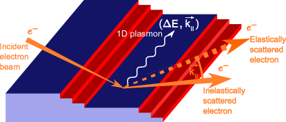
b) 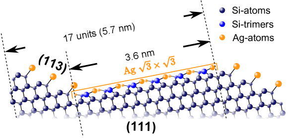
Recently, we presented results on 1D plasmon excitation in wires of -ordered Ag on Si(557) [20]. Although a coverage of one monolayer (1ML) was deposited, 1D dispersion was found, indicating electrical separation between quite densely packed atomic wires. The side view of the atomistic arrangement, using the honeycomb-chained trimer model for the (111)-terraces [21], is shown fig. 1b). Please note that the position of the Ag atoms on the (113) facets is not known and only sketched schematically. Interestingly, neither has the concentration dependence of the plasmon energy been tested for such 1D systems nor is the origin of conductance clear. For tests answering these questions the Ag-phase on the stepped Si(557) surface turned out to be well suited. Since no angular resolved photoemission (ARPES) photoemission data for this system are available yet, the analogy with the similar Ag/Si(111) system tells that the perfect Ag-phase might also be a semi-metal, as found for the monolayer of Ag on Si(111) [22, 23, 24], and tuning of the plasmon resonance by Ag concentration may be possible [25]. Here the Ag-modified surface state, , touches the Fermi level from above, but remains empty. Only by a surplus of Ag atoms, charge is transferred to this state so that it gets partially filled, leading also to the observability of 2D sheet plasmons [26]. In a recent publication [20], we showed that a similar phase is formed as -ordered wires of finite width on the (111)-oriented mini-terraces of the Si(557)-surface. Whereas a different kind of wires is formed at low coverage, ML, which turned out to be semiconducting, metallic conductance was found to be associated with the appearance of -ordered domains, as we demonstrated by high resolution electron energy loss spectroscopy (HREELS). A clear plasmonic loss was identified for this phase, which showed dispersion only in the direction along the wires. No dispersion, but only subband formation and intersubband-plasmon excitation was observed in the direction normal to the wires.
This metallicity is indeed caused by Ag atoms added to the perfect Ag-phase, as we demonstrate in this paper. It seems that a certain surplus of Ag atoms is always generated during the standard preparation procedure resulting in a conducting array of wires. As we show below, this excess concentration of Ag atoms can be eliminated by an annealing treatment without removal of the -ordered wires. This means that also for this stepped surface a mechanism seems to be operative that is similar to the Ag/Si(111) system. On the other hand, this mechanism also allows to vary the concentration of charge carriers. Here we again use the plasmonic losses as sensor, which allows to test the dependence of these losses on the Ag excess concentration. Since we are working in the low excess coverage regime ( ML), it seems plausible that a linear relationship between excess Ag concentration and charge carrier concentration,, holds. Thus we are able to test the dependence of the plasmon dispersion on in 1D via doping experiments.
2 Experimental setup
The plasmons were measured by using a combination of high resolution electron loss spectrometer (EELS) as electron source with a low energy electron diffraction system (LEED) providing simultaneously high energy and momentum () resolution [27, 28]. Typical operating parameters were 25 meV energy resolution at a resolution of . In order to check the surface structure after in-situ cleaning and after Ag adsorption profile analysis in LEED (SPA-LEED) was used. Ag was evaporated by electron-beam heating from a Molybdenum crucible. The Ag flux was controlled by a quartz microbalance located at the evaporator. This micobalance was calibrated with another one located at sample position, supplemented by calculated estimates and by STM. The different approaches agreed within 8%, but the direct microbalance calibration was considered to be the most reliable. The uncertainty of the latter was less than 5%. The coverage below is given with respect to the surface density of Si(111), i.e. 1 ML. The sample was prepared by repeated annealing cycles to 1100°C , which consisted of rapid heating to this temperature, a quench to 900°C , a linear cooldown to 800°C over 2 min before the sample was cooled down without further heating. Surface quality was subsequently checked with LEED. In order to determine accurately the peak positions of the plasmon losses, the spectra have been fitted. The elastic peak was modeled by a Gaussian peaks and an exponentially decaying Drude tail while the individual losses were modeled using an exponentially modified Gaussian (EMG) functions and a constant background.
3 Results and discussion
3.1 The reference Ag-structure
We first describe the generation of a Ag-reference structure. Here, the aim was to generate large and perfectly ordered -terraces with as little excess Ag concentration as possible on them. For our investigations, there is no need, however, that they cover the surface completely, since all parts of the surface not covered by this structure are semiconducting. Therefore, they do not contribute to the plasmon signal.
In a first step we evaporated 1.2ML Ag onto the sample held at 500°C . This results in formation of a R30∘ structure on the (111)-oriented terraces, which is completed at one monolayer coverage, with the typical elongated spots characteristic of stripes with this order and an average width of 3.6 nm [20] (see Fig. 2a). The 1.2ML Ag amount was chosen in order to start with a saturated structure and to be able to then carry out controlled desorption experiments [21, 29]. The excess coverage on the terraces and that on the (113) facets remains invisible in LEED, i.e. it is distributed randomly in very small islands, which were visible in STM.
In a second and crucial step, the Ag covered surface was heated periodically to 600°C for 60s via direct current parallel to the steps with a 10min cooldown. This procedure leads to partial desorption of Ag, but at the same time to complete removal of metallicity, as shown below, without losing the majority of -ordered terraces.
After heating cycle we performed SPA-LEED measurements (Fig. 2) to check the surface. The first heating process was controlled with a Pyrometer during which the current-voltage curve was measured. Using this information we were able to perform the same procedure at the same spot after exactly the same heating steps. The partial desorption of Ag without destruction of the Ag-structure is obvious from Fig. 2b) [29, 24, 30]. Whereas the superstructure remains intact after the heating cycles, its intensity is reduced, but the peak widths remain constant until the spots are close to disappearance. As can be estimated from the reduction of (integrated) LEED intensities in the -superstructure spots (Fig. 2d) that the loss of Ag coverage is about 0.15 ML per cycle. Thus the Ag-reconstruction is still covering the surface to about 85% after two cycles. This means that the surface consists of finite domains of -structure and semiconducting thin wires. After 6 heating cycles no Ag-spots remain, but only the streaks. There is no indication for reappearance of the reconstruction, i.e. the whole surface is still covered with the low-coverage species of silver induced atomic (and semiconducting) wires.
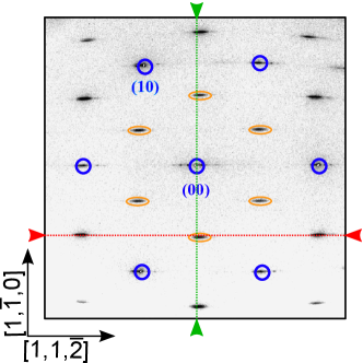
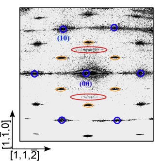
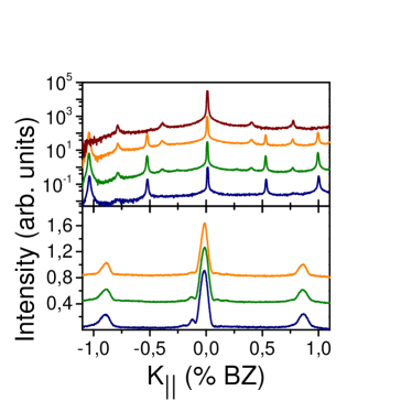
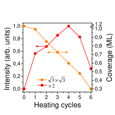
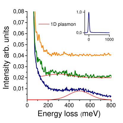
At the same time, the charge carrier concentration of Ag in the Ag-stripes is reduced, as seen by the HREELS spectra shown in Fig. 3. Already after the second heating cycle the plasmon cannot be detected any more. In fact, upon further heating cycles the loss spectra remain unchanged, and their shape is identical to that measured for an Ag concentration of 0.3 ML [20]. The latter concentration marks the onset of -island formation as a function of coverage, as detected by LEED. Below this concentration only semiconducting nanowires were observed both on the (111) and (113) facets [20], as already mentioned. These wires on both the (111) terrraces and on the steps are characterized by a double periodicity with respect to the Si substrate, which leads to - streaks in the LEED pattern (see Fig. 2b)) [20, 31]. During the heating cycles described above these streaks reappear already after the first heating cycle, as seen from Fig. 2c) and d). They are a signature of phase coexistence of - and atomic wire phases, which ends after six heating cycles. At this coverage only the semiconducting wire phase is left. The strongly non-monotonic intensity change of the streaks with a clear maximum after four heating cycles, however, cannot be explained by simple phase coexistence. It means that strong rearrangement mainly at the steps must occur during the first heating cycles, most likely due to preferential desorption of Ag at the steps.
For the remaining description of our experiments we concentrate on the properties of Ag layers after two heating cycles, which turned out to be sufficient to remove metallicity, as detectable by characteristic plasmon losses. From the measurements shown in Fig. 3 we can get an upper limit of the remaining doping of the Ag-nanowires. The detection limit of a plasmon, using quantitative fits of the loss spectra, is about 100 meV. As deduced from the dispersion measured in ref. [20], an electron concentration of cm-1 was found there. This resulted in a loss peak at 878 meV at 10%BZ. Assuming ( is the electron density), we reduced the electron concentration by at least a factor of , i.e. below cm-1.
Summarizing this section, we have found a way to bring back the Ag-layer into a semi-metallic or even semiconducting state, i.e. we have removed the Ag species below detection limit that is responsible for charge transfer into the Ag induced surface state. This was done at the expense of formation of an incomplete monolayer of Ag-. We note here that the re-appearance of mobile charge carriers, as detected by EELS-LEED recording the plasmonic losses, happens already at the smallest amounts of additional Ag, i.e. without any threshold in added Ag concentration. This will become evident from our experiments with Ag addition described below. Evenly important, our findings do not depend on the exact amount of remaining Ag-concentration after the heating cycles, i.e. they are a unique property of the Ag-structure.
3.2 Plasmon loss induced by residual gas
In the following we demonstrate that after the treatment of the Ag-layer, prepared as described above, with the complete removal of the characteristic plasmonic losses we are able to reverse this process both by adsorption of small amounts of Ag and even by adsorption of residual gas, i.e. we carried out “doping” of the Ag-layer. We first describe the effects by residual gas adsorption, since the influence of residual gas has to be taken into account for the quantitative determination of loss frequencies as a function of Ag concentration.
For this purpose, we took a freshly prepared sample with 1.2 ML of Ag and carried out two heating cycles to 600°C . Then we performed EELS-LEED measurements at constant with respect to the (00) spot, and restarted the measurement typically every hour, working at the base pressure in the system of mbar. The shift of the plasmon loss peak as a function of time is shown in Fig. 4a). In order to be able to plot several different into the same graph, and to combine different runs, we normalized the data to the saturation value for each . Interestingly, the saturation value of the plasmonic loss obtained by residual gas adsorption,, turned out to be very close to the value obtained after simple adsorption of 1.0 ML of Ag without heating the surface afterwards [20]. Please note that time zero is taken when measurements were started, which does not coincide with the effective start of residual gas adsorption, since several control measurements were carried out before the actual measurement was started. The typical time constant, as deduced from the fit described below, was found to be about 5 hours, in qualitative agreement with expectations of residual gas adsorption at this pressure. It should be noted here that these findings are not due to any mobility of Ag atoms on the surface, as concluded from the controlled adsorption of Ag described below.
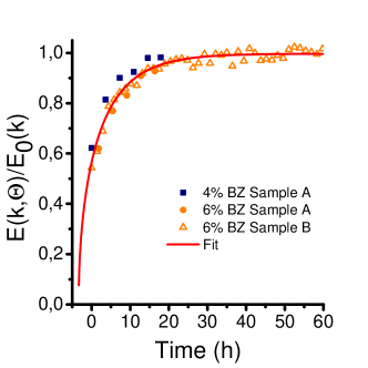
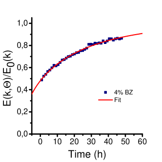
In fact, the change of plasmon loss energy as seen in Fig. 4a) can be almost quantitatively modeled (see red lines in this figure) by assuming that an incoming atom is only adsorbed if it hits a free adsorption site directly, and is reflected otherwise (Langmuir adsorption). This is reasonable, since adsorption of the typical constituent of the residual gas (CO, H2O, H2) will not be adsorbed on the Ag-covered (111) terraces, apart from defects. They may, however, be adsorbed at step sites. In any case, the time available for diffusion will be very short, so that direct adsorption is most likely. This model leads to a linear decay of the adsorption probability as a function of active site concentration, and an exponential saturation of the additional coverage with time. In order to come to a quantitative description of the observed adsorption behavior, we have to make two further assumptions: a) The additionally adsorbed atoms make a constant charge transfer per particle into the surface state, , and b) a square root like dependence between the plasmon energy and the electron density exists. while the first assumption can only be rationalized by the still low concentration of charge carriers (for an estimate, see below), the second is substantiated by further experiments with controlled amounts of Ag, described in the next section. We then obtain the following formula, which describes the time dependence of the plasmonic electron loss energy at constant , normalized to the respective saturation value:
| (1) |
The normalization by the saturation energy at each was done in order to remove the dependence on momentum and to be able to plot the data into a common graph, if the assumptions made above are fulfilled. represents the particle flux per unit area hitting the surface per time, and is the probability that a particle will stick on a previously empty site. represents the fraction of already occupied sites at .
As demonstrated by the red curves in Figs. 4a) and b), the data fall well on the red lines obtained from fits with eq. 1, where different time constants for the changes of were obtained, depending on the amount of Ag added to the freshly prepared Ag-surface after the heating cycles. Already an amount of 0.016 monolayers (ML) of Ag increases the time constant of the plasmonic shift induced by residual gas by a factor of 10. Therefore, the influence of residual gas on the results of Ag doping had to be subtracted only for the smallest Ag concentrations.
The reasonably good fit to the data seems to justify the assumptions made in the model leading to eq. 1. It contains several aspects: Apart from an indirect proof of the dependence of the plasmonic energy also in 1D, the model assumes, as mentioned, that the “dopants” are an immobile species adsorbed on defects and/or steps of the surface. Additional Ag atoms seem to compete for the same defect sites with residual gas particles and are able to effectively block them against residual gas. Taking the analogy to the results found on flat Si(111) [24], Ag atoms are expected to act as electron donors. Since the excess charge density at saturation is comparable to that found in our previous work [20], namely cm-1 per wire, we can easily estimate the density of particles necessary to produce this effect, assuming that one elementary charge per particle is transferred: The Ag-covered (111) terraces are 11 Si units wide. Along the wires we have an Si density of cm-1 per atomic row. The Ag density in the Ag-phase is the same as for Si. Assuming that the line density of charges determined above is evenly distributed among the Ag atoms in the phase, this corresponds to about 0.066 elementary charges per Ag atom on the (111) terrace. It is quite unlikely that the density of defects fixing the charge transferring particles within the Ag-wires is so high as to provide this charge density. On the other hand, a single atomic chain with the Si density at a step edges adjacent to (111) terraces may provide a density of sites that is sufficient for adsorbing the amount of particles necessary for doping.
The strong change in time constant by pre-doping with Ag indicates that Ag passivates not only the occupied site but also its nearby surrounding by repulsive interactions with residual gas particles. In fact, Ag atoms turned out to be highly mobile at room temperature on the Ag-/Si(111) terraces [32]. Therefore it is quite likely that these atoms are only trapped at the step edges, where they become immobilized. Attempts to identify the adsorbed species directly by characteristic vibrational losses turned out not to be successful, presumably for reasons of low concentration.
3.3 Doping via adsorption of silver adatoms
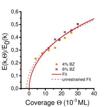
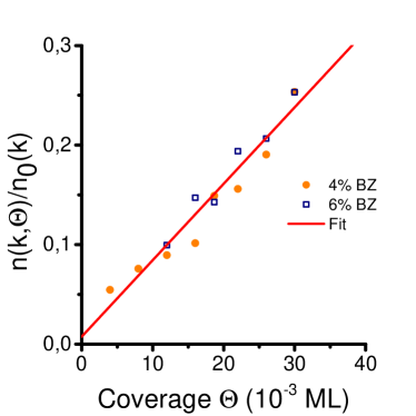
While these experiments demonstrate the effect of charge transfer by adsorbed species qualitatively, we now go one step further by directly using the adsorption of Ag atoms on a Ag--ordered surface, prepared as described above, that shows no plasmonic losses. Here the amount adsorbed is well known due to our calibration. After preparation of 1.2 ML of Ag, we again carried out two heating cycles and then evaporated various small amounts of silver with the sample held at RT, followed by EELS-LEED measurements at several scattering angles with respect to the (00) beam, i.e. at various . Effects of residual gas adsorption have been carefully subtracted from the measured loss energies, but their influence could be kept small in all cases. In Fig. 5a) we show results of measured loss energies as a function of Ag exposure to the sample in units of ML. In the small excess coverage range, , considered here (up to 3% of a monolayer) the assumption of a constant sticking coefficient, which must be close to 1, seems to be well justified. Thus coverage and total charge carrier concentration are linearly related. Similar to the data treatment in Fig. 4, we normalized the loss energies by the value obtained after preparation of 1.0 ML [20] without further treatment for each in order to combine data at different . Data at 4 and 6% BZ are shown. As seen in Fig. 5a), the plasmonic energy losses are fully compatible with a behavior that goes through zero at zero excess coverage, , i.e. without offset.
This means that
a) the Ag-wires as prepared by our heating cycles are indeed semi-metallic.
b) The additional Ag atoms adsorbed afterwards are responsible for an effective charge transfer
into the surface band, which gets partially filled due to the charge provided by the excess Ag atoms.
c) As seen in Fig. 5b), which plots the normalized square of a), a linear slope as a function of
is obtained. This is expected for a constant charge transfer per excess Ag atom and for a dependence of the plasmonic loss energy.
Therefore, we conclude that this functional dependence is also valid for 1D plasmons.
There is, of course, still the open question whether all adsorbed excess Ag atoms will contribute to the charge density in the surface band. Furthermore, it is unclear where these excess atoms are located. In order to answer these questions we carried out EELS measurements at different temperatures between 80 and 400 K after preparation at RT. The plasmon losses generated by the excess Ag atoms turned out to be completely temperature independent. This finding rules out any phase equilibrium between a disordered lattice gas on top of the Ag-wires as suggested for the Ag/Si(111) system [25]. It means that these excess atoms must be trapped and immobilized, i.e they are also chemisorbed quite strongly. The adsorption must be less strong than for the atoms in Ag-wires, even at their edges, since we were able to preferentially desorb the excess atoms. Therefore, they cannot simply be edge atoms of the Ag-wires. Most likely, they occupy sites at the steps adjacent to the Ag-wires. Since bond formation there is different from the flat (111) terraces, dipole formation associated with charge transfer is possible. This conclusion is consistent with the finding that the Ag atoms on top of the Ag-wires are highly mobile at room temperature [33], so that they will be able to diffuse quickly into the stepped areas where they are trapped. The temperature independence of our findings over a very wide range of temperature indicate that thermal activation for diffusion plays no role. Therefore, we can safely assume that essentially all adsorbed excess Ag atoms contribute to the charge transfer leading to 1D plasmon formation.
The induced electron density responsible for the plasmonic excitation can now be easily calculated via the change of the 1D plasmon energy for constant momentum
| (2) |
In Fig. 5b) we plot again the normalized values, where was again taken from the data of the 1.2ML Ag layer (cm-1). As seen in Fig. 5b), we get an electron concentration of about 23% of by adsorbing 30 ML of Ag.
From the discussion above we concluded that the excess Ag atoms are concentrated on the steps of the (557) surface. There are two steps without direct contact to the Ag-stripes. If these are the adsorption sites, we find that the homogeneous adsorption of 30 ML of Ag on the whole surface, concentrated into two atomic chains, results in an average atomic density of cm-1 in the two chains. The electron density after excess doping by 30 ML of Ag obtained from Fig. 5b) is cm-1. Thus we estimate the electron transfer rate to be around 1/3 of an elementary charge per Ag atom. It is obvious that this number can only be taken as a preliminary estimate that relies on assumptions still to be tested in more detail. Such investigations are in progress.
4 Summary and conclusions
In this paper we gave evidence for the fact that, similar to the Ag/Si(111) system, also Ag-wires on Si(557) are semi-metallic. The Ag-induced surface state can, however, be made conducting by appropriate charge transfer, which can be done by components of the residual gas, most likely water, and - more quantitatively - by adsorption of excess atoms of Ag on the Ag-phase. A doped phase, and thus a metallic array of wires, turns out to be always generated by the standard procedure of preparation. We thus proved a doping mechanism to be effective for a quasi-1D system. All excess particles leading to doping could be removed by thermal treatment of the sample.
Our proposed mechanism for charge transfer is not the standard mechanism of intrinsic doping, since it is effective also with the same species as that which forms the wires. It relies on the variability of chemical bond formation in locally different environments with corresponding charge transfer into the bands formed by the majority species. Secondly, the doping generated by this mechanism is extrinsic on the atomic scale in the sense that the doping material is not incorporated into the Ag wires.
Quantitative dosage of excess Ag atoms showed that the concentration of excess charges depends linearly on excess Ag concentration, if a dependence of plasmonic loss energies is assumed, as predicted by theory [34]. This theory, however, is based on the nearly-free electron gas model that is not expected to be valid in 1D, but this square root dependence on seems to survive.
Estimates show that only a fraction of an elementary charge is transferred, as expected for a mostly covalent bond formed between Ag and Si. If other species like water or OH allow a higher charge transfer, the amounts necessary for the observed charge concentrations (only a few percent of a monolayer) may not easily be detectable by EELS for intensity reasons.
References
References
- [1] Barnes W, Dereux A and Ebbesen T W 2003 Nature 424 824
- [2] Maier S 2007 Plasmonics: Fundamentals and Applications (Springer, Heidelberg)
- [3] Bergman D J and Stockman M I 2003 Phys. Rev. Lett. 90 027402
- [4] Marell M, Smalbrugge B, Geluk E J, van Veldhoven P, Barcones B, Koopmans B, Nötzel R, Smit M and M T Hill Opt Express 19 2011 Opt. Express 19 15109
- [5] Yan H, Low T, Zhu W, Wu Y, Freitag M, Li X, Guinea F, Avouris P and FXia 2013 Nature photonics 7 294
- [6] Tegenkamp C, Pfnür H, Langer T, Baringhaus J and Schumacher H W 2011 J. Phys.: Condens. Matter 23 012001
- [7] Pfnür H, Langer T, Baringhaus J and Tegenkamp C 2011 J. Phys.: Condens. Matter 23 113204
- [8] Silkin V M, Garcia-Lekue A, Pitarke J M, Chulkov E V, Zaremba E and Echenique P M 2004 Europhys. Lett. 66 260
- [9] Morawitz H, Bozovic I, Kresin V, Rietveld G and van der Marel D 1993 Z. Phys. 90 277
- [10] Diaconescu B, Pohl K, Vattuone L, Savio L, Hofmann P, Silkin V M, Pitarke J M, Chulkov E V, Echenique P M, Farias D and Rocca M 2007 Nature 448 57
- [11] Park S and Palmer R 2010 Phys. Rev. Lett. 105 016801
- [12] Pohl K, Diaconescu B, Vercelli G, Vattuone L, Silkin V M, Chulkov E V, Echenique P M and Rocca M 2010 Europhys. Lett. 90 57006
- [13] Jahn M, Muller M, Endlich M, Neel N, Kröger J, Chis V and Hellsing B 2012 Phys. Rev. B 86 085453
- [14] Vattuone L, Smerieri M, Langer T, Tegenkamp C, Pfnür H, Silkin V, Chulkov E V, Echenique P M and Rocca M 2013 Phys. Rev. Lett. 110 127405
- [15] Sarma S D and Lai W 1985 Phys. Rev. B 32 1401
- [16] Inaoka T 2005 Phys. Rev. B 71 115305
- [17] Rugeramigabo E P, Tegenkamp C, Pfnür H, Inaoka T and Nagao T 2010 Phys. Rev. B 81 165407
- [18] Nagao T, Yaginuma S, Inaoka T, Sakurai T and Jeon D 2007 J. Phys. Soc. Japan 76 114714
- [19] Block T, Baringhaus J, Tegenkamp C, Inaoka T and Pfnür H 2011 Phys. Rev. B 84 205402
- [20] Krieg U, Brand C, Tegenkamp C and Pfnür H 2013 Journal of Physics: Condensed Matter 25 014013
- [21] Wan K J, Lin X F and Nogami J 1993 Phys. Rev. B 47 13700
- [22] Ding Y, Chan C and Ho K 1991 Phys. Rev. Lett. 67 1454
- [23] Zhang H M, Sakamoto K and Uhrberg R I G 2001 Phys. Rev. B 64 245421
- [24] Crain J N, Gallagher M C, McChesney J L, Bissen M and Himpsel F J 2005 Phys. Rev. B 72 045312
- [25] Liu Y and Willis R 2009 Surf. Sci. 603 2115
- [26] Nagao T, Hildebrandt T, Henzler M and Hasegawa S 2001 Phys. Rev. Lett. 86 5747
- [27] Claus H, Büssenschütt A and Henzler M 1992 Rev. Sci. Instr. 63 2195
- [28] Nagao T and Hasegawa S 2000 Surface and Interface Analysis 30 488
- [29] Ueno M, Matsuda I, Liu C and Hasegawa S 2003 Jap. J. Appl. Phys. 42 4894
- [30] Uhrberg R I G, Zhang H M, Balasubramanian T, Landemark E and Yeom H W 2002 Phys. Rev. B 65 081305
- [31] Morikawa H, Kang P G and Yeom H W 2008 Surf. Sci. 602 3745
- [32] Sato N, Nagao T and Hasegawa S 1999 Phys. Rev. B 60 16083
- [33] Hasegawa S, Sato N, Shiraki I, Petersen C L, Bøggild P, Hansen T M, Nagao T and Grey F 2000 Jap. J. Appl. Phys. 39 3815
- [34] Li Q and Sarma S D 1990 Phys. Rev. B 41 10268