Electronic structure of stacking faults in hexagonal graphite
Abstract
We present results of self-consistent, full-potential electronic structure calculations for slabs of hexagonal graphite with stacking faults and for slabs with one displaced surface layer. There are two types of stacking faults, which differ qualitatively in their chemical bonding picture. We find, that both types induce localized interface bands near the symmetry line K-M in the Brillouin zone and a related peak in the local density of states (LDOS) very close to the Fermi energy, which should give rise to a dominating contribution of the interface bands to the local conductivity at the stacking faults. In contrast, a clean surface does not host any surface bands in the energy range of the and bands, and the LDOS near the surface is even depleted. On the other hand, displacement of even one single surface layer induces a surface band near K-M. A special role play -bonded dimers (directed perpendicular to the layers) in the vicinity of one type of stacking faults. They produce a half-filled pair of interface states / interface resonances. The formation energy of both types of stacking faults and the surface energy are estimated.
pacs:
73.21.Ac, 73.22.Pr, 73.20.At, 81.05.U-I Introduction
Graphitic systems gained a renewed interest (after the intercalation, fullerene, and nanotube rushs) following the invention of techniques to produce thin two-dimensional systems in the form of thin slabs or even mono-layers (for recent review see e.g. Refs. Neto et al., 2009; Abergel et al., 2010; Peres, 2010; Goerbig, 2011). There is, however, another form of two-dimensionality, namely stacking faults in bulk hexagonal (AB) graphite with related interface states. These states are interesting, because they have been suspected to play a role in the observed integer quantum Hall effect Kempa et al. (2006); Arovas and Guinea (2008) in bulk graphite. As we will show, they may also contribute considerably to the electronic conductivity.
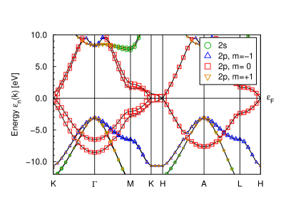
The electronic states in graphitic piles can be grouped into and states. The bands are mainly formed by orbitals, they are responsible for the electronic structure around the Fermi energy . The bands with a total band width of about 40 eV are formed by the three linear combinations of , and orbitals and lie more than 3 eV below and more than 8 eV above (see Fig. 1). It is mainly the bands which stabilize the honeycomb structure of the graphene layers, while the bands account for their intriguing physical properties.
The importance of the electronic structure of stacking faults in graphite results from their abundance in all kinds of samples and from the fact that they host localized interface bands Arovas and Guinea (2008); Koshino and McCann (2013). The large probability of their occurrence has its origin in the small energy difference between different stacking sequences, which for its part can be traced back to the large difference between intra-layer and inter-layer overlap integrals. The largest interlayer overlap integral between orbitals, , is 0.4 eV, and the largest intra-layer overlap integral between orbitals, , is 2.6 eV Brandt et al. (1988); Grueneis et al. (2008). The overlap integrals between orbitals are not included in the common tight-bonding models. It follows from the large gap and bandwidth, that they are much larger than .
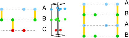
Fig. 2 shows the three possible highly-symmetric relative locations of graphene layers within a hexagonal unit cell. In constructing stacking faults, we consider slabs of AB-stacks (which would form hexagonal graphite, if the slab was infinite), followed by a C-layer, whereby the C-layer is already part of the subsequent CA- or CB-stack. In this way, two kinds of stacking faults are generated (see Sect. IV). Generally, we rule out the neighborhood of two identical layers, because of their large contribution to the total energy (see Charlier et al. (1994) and our results below). Such a slab with a stacking fault is either periodically repeated (without any surface), or surrounded by slabs of vacuum and then periodically repeated. In the latter case we can study interfaces and surfaces in the same calculation. In case of periodic repetition without vacuum we have the advantages that the unit cell can be chosen to have a higher symmetry than a slab, and that the large surface energy does not mask the small total energy differences between the two types of stacking faults. Therefore, total energies of stacking faults were calculated in the geometry without surfaces, but one-electron spectra and surface energies in slabs with surfaces. Additionally, we considere pure AB-slabs with surfaces (see Sect. III) and with a single displaced surface layer of type C on either side (see Sect. VI). The width of the vacuum layer was chosen to be 6 interlayer distances throughout this paper.
Two previous works on stacking faults Arovas and Guinea (2008); Koshino and McCann (2013) considered two phenomenological overlap integrals ( and ) within a mostly analytical model calculation. While this model correctly predicts the existence (not the details) of interface bands at one of the two possible stacking faults in hexagonal graphite, it cannot describe the band structure around of hexagonal (Bernal) or rhombohedral bulk graphite even qualitatively (see Ref. Koshino and McCann, 2013 and references therein). Former self-consistent slab calculations on graphitic slabs can be found in Refs. Latil and Henrard (2006); Aoki and Amawashi (2007); Min et al. (2007); Zhang et al. (2010); Xiao et al. (2011).
In this paper we present results from self-consistent full-potential local-orbital calculations using the FPLO-package fpl ; Koepernik and Eschrig (1999). All calculations use density functional theory (DFT). Total energies of stacking faults are calculated within the local density approximation (LDA) (PW92 Perdew and Wang (1992)). The LDA has been chosen for the total energy, because it benefits from a cancellation between the over-binding (characteristic for the LDA) and the neglected van-der-Waals interaction. By minimizing the total energy the LDA provides rather precise values for the lattice constants of hexagonal graphite (see Charlier et al. (1994) and our results below). For the one-electron spectra we used the generalized gradient approximation (GGA) (PBE96 Perdew et al. (1996)), because the LDA fails to reproduce the characteristic four-leg structure of the electron pocket in hexagonal bulk graphite (see Sect. II). The GGA, on the other hand, which in many cases provides more accurate lattice constants than the LDA, fails to describe the binding between graphene layers (see also Ooi et al. (2006)). All calculations on one-electron spectra were done with the experimental C-C distance within the layers of 1.42 Å and an interlayer distance of 3.33 Å Aoki and Amawashi (2007). The lattice constants from total energy calculations are separately discussed in the text.
Band weights represent the size of the contribution of local orbital to the Bloch wave function . The sum of all orbital weights is normalized to unity
| (1) |
In the plots with band weights,
the local orbitals are represented by the form and color
of symbols
at the energy bands, and the band weights by the size of the symbols.
Because for bulk states the band weights converge to constants
away from surfaces/interfaces,
it follows from the sum rule (1) that
scales like ,
where and are the number of atoms in a layer and the number of layers in a slab, respectively.
For surface / interface states the band weights converge to zero,
and consequently the band weights scale like .
This means that for bulk states the band weights at each site are decreasing
with growing slab thickness, whereas for surface / interface states they
become independent of the thickness. For thick slabs the largest
band weights for
surface / interface states (in the vicinity of the surface / interface)
are therefore much larger than for bulk states.
The local density of states (LDOS) is defined as
| (2) |
and integrates to 2 electrons. All space integrations were done with the tetrahedron method Lehmann and Taut (1972, 1973).
II Bulk graphite
II.1 Band structure
Despite the fact that hexagonal bulk graphite has already been the subject of numerous works (see e.g. reviews on older work Kelly (1981); Brandt et al. (1988), and the more recent self-consistent calculations using LDA, GGA, and GW Charlier et al. (1991, 1994); Ooi et al. (2006); Grueneis et al. (2008)), we have to say a few words about it. This is because we want to demonstrate the results of our approach in the bulk limit, and to introduce the projected bulk band structure (PBBS) of hexagonal graphite. If not otherwise indicated, the k-mesh for the self-consistent calculation on bulk hexagonal graphite comprises 500x500x100 inequivalent points distributed equidistantly over the Brillouin zone (BZ).
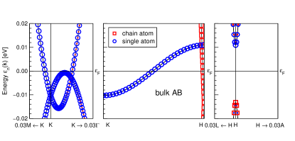
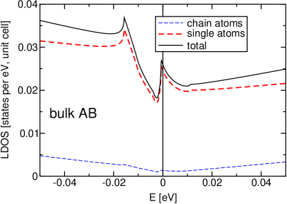
Fig. 1 gives an overview over the bulk band structure in GGA showing that lies in a gap of the -bands of width 11 eV and that all the Fermi surface physics comes from bands. Perpendicular to the layers, bulk hexagonal graphite consists of linear chains of atoms with overlapping orbitals and single atoms (monomers) with dangling bonds (see Fig. 2). Fig. 3 and Fig. 4 show that it is mainly the single atoms which carry the states around . In particular, the states of the degenerate very flat band with 20 meV dispersion between K and H carry only weights from the single atoms (Fig. 3). The other bands with about 1 eV dispersion between K and H carry only weights from the chain atoms. The small dispersion of the single-atom bands is due to their dangling bonds. The two peaks in the LDOS near in Fig. 4 are produced by the two extrema seen in the left panel of Fig.3, which refers to the central plane of the BZ at =0.
Our Fermi surface (FS) in GGA shows the generally accepted four-leg topology of the majority electron- and hole pockets, which are located correctly within the BZ. The only qualitative difference in our LDA results (not shown) is that the maximum of the downward bent parabola in the left panel of Fig. 3 lies slightly (by 0.5 meV) above . This tiny shift has the consequence that the electron pocket decomposes into 4 pieces, just as reported in the LDA approach by Ref. Charlier et al. (1991). Therefore, we used the GGA for the calculation of all one-particle spectra.
In the literature there has been a lengthy debate about the number and location of tiny minority pockets, which depend sensitively on the sign and size of the small overlap integrals (mainly ) of the Slonzewski-Weiss-McClure (SWM) model Slonzewski and Weiss (1958); McClure (1957) (see review Brandt et al. (1988)) and, from the experimental side, on the characteristics of the samples. Even recently appeared papers on the interpretation of the de Haas - van Alphen data Luk’yanchuk and Kopelevich (2004); Sugawara et al. (2006) indicating that the matter is still in discussion. With our DFT calculations we did not find any minority pockets, which seems to be a general trait of self-consistent DFT and GW calculations Charlier et al. (1991); Grueneis et al. (2008). This problem can be fixed by introducing artificial doping Grueneis et al. (2008), but we did not take any measures in order to make the FS agree with the SWM model in the issue of the tiny minority pockets.
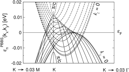
II.2 Projected bulk band structure
The PBBS is a useful tool to separate surface- or interface bands of thick slabs from bulk bands without investigating all slab wave-functions in detail, but just by locating their energy relative to the PBBS. The PBBS is defined as follows: Assume that the slabs to be investigated extend in the plane and calculate the bulk band structure (BBS) with macroscopic periodic boundary condition in all 3 dimensions. Then plot for all and for a quasi-continuous set of values:
| (3) |
The resulting distribution will show broad quasi-continuous bands and gaps (see Fig. 5 in case of hexagonal graphite for 11 values).
For bands in slabs in the limit of infinite thickness (but without
periodic macroscopic boundary conditions in -direction)
the following statements hold Heine (1962):
(i) Slab bands which lie in gaps of the PBBS are surface- or interface
bands localized in direction toward the interior of the slab.
(ii) Slab bands which lie in (quasi-continuous) bands
of the PBBS agree exactly in energy with the corresponding band of the BBS,
and their density agrees in the interior
of the slab with that of the bulk bands.
(iii) Slab bands within a gap, but close to the edge of a (quasi-continuous)
band of the PBBS, have weak localization (large decay length).
Of course, numerical slab calculations are done on slabs of finite thickness. In case of any reasonable doubt concerning the character of the band, if slab bands are very close to band edges of the PBBS, one can obtain certainty only by analyzing the spatial localization of the slab wave-function, e.g., by calculating the band weights.
II.3 Total energy
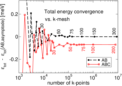
In order to check the possibility to use the LDA for total energy calculations of graphitic systems we first calculated the optimized lattice constants of bulk (AB) and (ABC) structures and compared their total energies. Despite the missing van-der-Waals correction, we observe in Table 1 still some overbinding characteristic of the LDA, but all in all, the LDA does well for the lattice constants. From Table 2 we can learn that the total energies of hexagonal (AB) and rhombohedral (ABC) graphite are very close in energy, whereas hypothetical hexagonal (A) stacking is well above. The latter result justifies the neglect of stacking orders with two identical neighboring layers for realistic sytems. However, (ABC) has a lower energy than (AB) despite the fact, that natural graphite is predominantly (AB) ordered. Because the energy difference is less than one meV, we not only did these total energy calculations with an increased numerical precision of the overlap integrals not and checked the convergence in the number of points carefully (see below), but we tried also the GGA, the LDA with Perdew-Zunger XC, and we added an extra shell of orbitals to the default basis set. None of these modifications reversed the ordering of the energies or changed essentially the energy difference. Consequently, either the correct energetic order of (AB) and (ABC) graphite is beyond the possibilities of the LDA and the GGA, or, the electronic part of the total energy in (ABC) is really lower than in (AB), but the here disregarded phononic part plays a decisive role for the ground state. In principle, there is also the possibility that the larger probability for (AB) ordering in natural graphite is due to special crystal growing conditions (temperature, pressure, etc.) and that (AB) graphite is a meta-stable state under ambient conditions like diamond.
The authors of Ref. Charlier et al. (1994) obtained for (AB) a total energy, which lies 0.1 meV below the total energy of (ABC) graphite. They however used the Monkhorst-Pack procedure with 28 special points (in the irreducible BZ) amounting to some hundred points in the full BZ. Fig. 6 shows, that up to some 10 000 (equidistant) points for the tetrahedron method the total energies for both structures oscillate wildly making a save calculation of such a small energy difference impossible. It is clear that the Monkhorst-Pack procedure has another convergence behavior than the tetrahedron method, but on the other hand it is not clear at all, whether it is suited for high precision demands on semi-metals like (AB) graphite, because it is tailored for semi-conductors and insulators.
| system | exp. | opt. | |
|---|---|---|---|
| (AB) | a | 2.4595 | 2.450 |
| 3.33 | 3.306 | ||
| (ABC) | a | 2.450 | |
| 3.305 |
| system | exp. | opt. |
|---|---|---|
| (AB) | 0 | -1.1 |
| (ABC) | -0.2 | -1.2 |
| (A) | +15.7 |
II.4 Estimate of the van-der-Waals correction
In order to find out, if the consideration of the van-der-Waals interaction can clarify the situation, we estimated its impact on the total energies using the semi-empirical approach by Grimme et al. Grimme (2011) in the version DFT-D2 Grimme (2006):
| (4) |
with the damping function
| (5) |
The sum runs over inter-atomic distances (calculated from experimental lattice constants of (AB) graphite) , the scaling factor is , , and for carbon the dispersion coefficient and the van-der-Waals radius amount to and , respectively.
We took into account only inter-layer contributions, because the intra-layer contributions are independent of the stacking sequence. It turns out, that the Grimme correction per atom to the total energy of bulk (AB) and (ABC) amounts to -210.4284 and -210.4289 meV, respectively, providing a difference of 0.5 eV in favor of (ABC) graphite. One reason for this minute difference is the fact that the interaction energy of two layers is independent of their type (provided they are not identical) and therefore only next-nearest (and beyond) layer interactions contribute to the energy difference between two stacking orders. Second, even if there is a difference, it is minute. There are only two values for the interaction between two arbitrary layers depending on whether they are identical (say A-A) or different (say A-B). The interaction energy of the two atoms in layer A with a full layer A for next nearest neighbor layers is 12.161923 meV versus 12.161918 meV for A-B. Consequently, the van-der-Waals correction at least in the semi-empirical Grimme form can be safely neglected for the energy difference between stacking orders.
III Surface of graphite
Graphitic slabs are numerically demanding in three ways:
(i) Because graphite is a semi-metal with a tiny Fermi surface around
the K-point, one needs a large number of points in order to get the
essential features of the FS well resolved and an accurate position
of the Fermi level.
For the self-consistent calculation we used a grid of
240x240x1 inequivalent points.
For the LDOS near we chose a special grid of points,
which is restricted to the vicinity of the K-point and comprises
150x150x1 points.
(ii) Due to the small density of states near
the screening of perturbations may extend over long distances.
Thus, the slabs used in the numerical calculation have to be choosen
rather thick, if separated interfaces or surfaces shall be described.
For slabs, which are thick enough, extra layers within the given building
scheme should not have an impact on the physical results.
(iii) Thick slabs with low symmetry tend to have problems
in converging to self-consistency. Therefore, it is vital to use the
highest possible symmetry.
This can be achieved
by choosing an appropriate number of layers (see Sect. IV-VI).
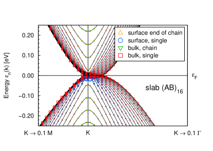
III.1 Band structure of (AB) slabs
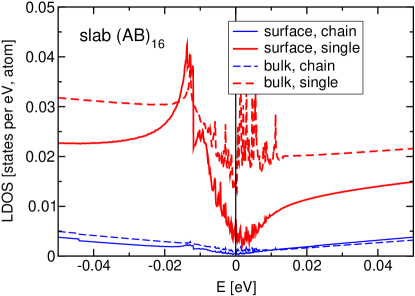
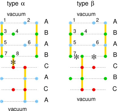
We consider a clean surface, which can be studied by means of a thick slab. Fig. 7 shows band weights in (AB)16 for a few prominent local orbitals and Fig. 8 presents the corresponding LDOS. For a visualization of the atomic positions in the slab see the right part of Fig. 2. As to -bonding, which is crucial for the electronic structure around the Fermi energy, we again distinguish single atoms (monomers) and chains, which are now finite.
First, in Fig. 7 we observe no
low-energy surface bands separated from the bulk continuum.
This refers to higher energies in the range of the and bands
on the symmetry lines as well (not shown in our figures)
in accordance with Ref. Ooi et al. (2006).
In contrast, the LDOS in Fig. 8 reveals that
around there is a depletion of
electrons in the surface layer rather than
an accumulation (which would be expected for surface states).
It should be expected that the bulk LDOS
in Fig. 8 converges to the
bulk curves shown in Fig. 4
in the limit of infinite thickness of the slab.
This is already suggested by Fig. 8,
except for the peak just above the Fermi energy ,
which is decomposed into a bunch of single peaks.
Closer inspection of the band structure
in the energy region around (not shown) reveals that
these peaks are mainly due to van-Hove singularities caused by avoided
crossing of bands, which gradually
disappear if the number of bands goes to infinity.
Second, Fig. 8 also shows that
the bands near are mainly localized at the single atoms.
Considering the results of the previous paragraph,
the latter conclusion is not surprising because the band structure
of a thick slab must be similar to the PBBS, if no
surface bands exist. Fig. 8 shows that
the LDOS around at single atoms in the bulk
is one order of magnitude larger than at chain atoms
in agreement with the bulk calculation in Fig. 4.
In terms of the local conductivity these two points lead to the conclusion that one should expect a depletion of conductivity in the surface layer and current flow mainly through hopping between single atoms. The strong asymmetry regarding the two atomic positions at the surface in the LDOS near the Fermi energy explains also the strong asymmetry of the two sites in STM images Tomanek et al. (1987).
III.2 Surface energy
We use the standard definition of the surface energy per surface atom
| (6) |
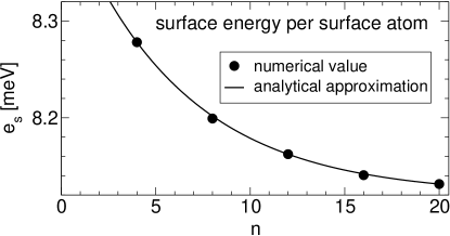
where is the total energy of the super-cell with atoms and is the total energy per atom for the bulk. Because each super-cell has two surfaces and two surface atoms on either surface, we introduced the factor in the definition. In principle the result of Eq. (6) might depend on the thickness of the layer, but has to converge in the limit of infinite thickness, provided, is calculated in the interior of the slab with the same precision as Boettger (1994). We met this demand by using the same program with the same parameters and the same grid in the plane parallel to the layers (120x120x50 and 120x120x1 for the bulk and the slabs, respectively). Our results shown in Fig. 9 are not yet fully converged, but a tendency toward convergence is obvious. In order to obtain an approximate asymptotic value , we adapted the three parameters of the ansatz to the three calculated values at = 4, 12, and 20, where our slab (AB)n consists of formula units. We found meV, meV, and . The corresponding curve is plotted in Fig. 9. Experimental values for (AB) graphite lie in the wide range of (2.83 - 18.9) meV/surface atom (see Table 5 in Ooi et al. (2006)) and the result for using Eq. (6) and the VASP code is 7.92 meV/surface atom Ooi et al. (2006).
Although we cannot reach full numerical convergence of with layer thickness, it is worthwhile to compare surface energies for the surfaces of (AB) and (ABC) graphite for the same number of layers. Calculations for slabs with super-cells (AB)6 and (ABC)4 (both have 12 layers) provide meV and meV, respectively. From a local point of view the smallness of the difference between the two systems seems understandable, because both surfaces differ only in the third layer from the surface inward. On the other hand, both systems differ qualitatively in their electronic structure. Whereas (ABC) graphite has around topologically protected surface states and a Dirac-like band structure in the bulk limit Xiao et al. (2011), (AB) graphite is a semi-metal with a small Fermi surface and without surface states in the whole region of and bands.
IV Stacking faults
For the calculation of one-particle energies and derived properties we used a periodic arrangement of slabs which are surrounded by vacuum and which have one stacking fault in the middle. The alternative model is a periodic arrangement (without vacuum) with two stacking faults per unit cell in order to obtain periodicity, which has been adopted for total energies (see Introduction). We want to stress that for the size of slabs presented here there is no remarkable difference between both models in the local properties like LDOS and band weights for atoms close to the stacking faults. All self-consistent calculations on slabs have been done with a mesh of 120x120x1 points equal-distantly distributed over the BZ. Test calculations with 240x240x1 points did not show any visible changes. For the calculations on periodically repeated super-cells we used a grid of 150x150x10 points.
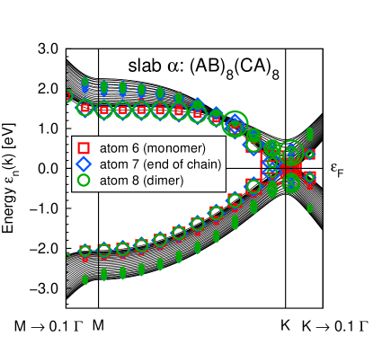
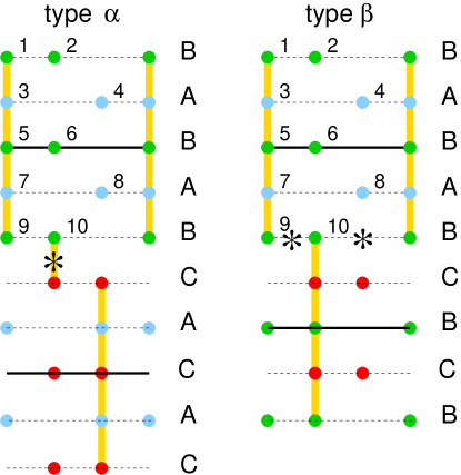
Fig. 10 gives the essential structural information on the two possible types of stacking faults in hexagonal graphite, denoted and . The number of layers has been chosen in such a way that the highest possible symmetry (and therefore precision for given computational resources) could be achieved. Whereas bulk hexagonal (AB) graphite has two Wyckoff positions, namely single atoms (monomers) and atoms on infinite chains with saturated orbitals, the chains are terminated at the surface and the interfaces ending with dangling bonds. The crucial difference as to local bonding between type and interfaces is the following: Type has a dimer bridging the stacking fault, with a related small interlayer overlap and indirect overlap between the chains on both sides of the fault via the dimer. In type , the dangling bonds of two adjacent chains overlap laterally with the large overlap integral .
IV.1 Band structure
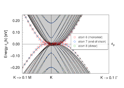
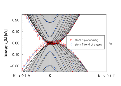
Figs. 11 and 12 show the energy bands with the most prominent band weights for and interfaces around the K-point. We observe that for both interfaces there is an occupied and an empty interface band close to the bulk continuum, except in the very vicinity of the K point. In either case, the interface bands are located mostly at the monomers closest to the interface (atom # 6 in Fig. 10), i.e., they are formed by the dangling -bonds of these monomers. The band weights of the monomers further away from the interface (e.g. # 4 in Fig. 10) in the interface bands are already small and would not be visible in these figures. This means that the amplitude of the interface bands converges rapidly to zero toward the bulk. Exceptions are the interface bands on the line K- in type . Their distance from the bulk continuum is smaller and their localisation is weaker than for the other interface bands. Therefore, the existence of an interface state in this region in the limit of infinite thickness is not absolutely certain.
Comparison of our results for type with the model calculations in Refs. Arovas and Guinea (2008) and Koshino and McCann (2013) shows little similarity apart from the mere existence of interface states. The main difference is that in our calculation the interface states vanish in the very vicinity of the K-point due to the presence of bulk states. The low-energy dispersion of these bulk states is not correctly described by simple models with only two overlap parameters.
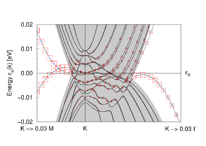
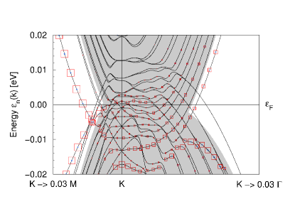
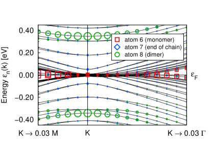
Fig. 13 shows another interesting feature. There are occupied and empty bands localized at the dimers of interface , which are split by approximately 0.8 eV at the K-point (see lower panel). This splitting agrees with the value, which is expected for the splitting of the levels in an isolated dimer due to an empirical overlap integral with the generally accepted value eV. Near the K-point, these dimer bands are no strictly localized interface bands, but resonances with a large amplitude near the interface, because they are submerged into the the continuum of bulk states. The upper panel shows, that along the line from K toward M not only the dimer atoms get involved in the interface bands, but also the atoms at the end of the chains. Therefore, away from the K-point and at energies of the eV-range, the interface bands are no longer localized solely at monomers. Inspection of the other parts of the 2D BZ (which are not shown in the figures) shows that on the symmetry lines interface states are only found on the line K-M and on small parts of the lines M- and K-. In other words, they are virtually restricted to the symmetry lines shown in the upper panel of Fig. 13.
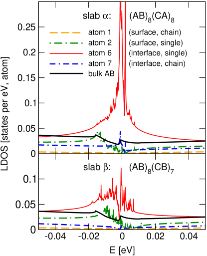
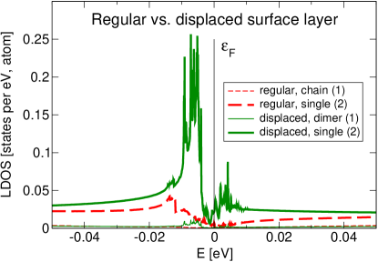
Fig. 14 presents the LDOS near both types of interfaces and near the surfaces compared with the bulk DOS. In either case the interface bands produce strong low-energy peaks in the LDOS for the monomers closest to the interface, but in type the peak is most pronounced.
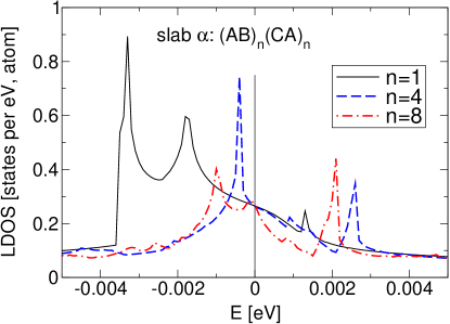
Fig. 15 presents the LDOS of slabs with interface for different thickness of the slab. One notes that even a slab with one graphite unit cell on both sides of the stacking fault (n=1) shows a pronounced peak and is thus a suited model for studying the interface bands, although the specifics of the low-energy electronic structure depend on the slab thickness, which is seen in the form of the LDOS.
IV.2 Formation energy of stacking faults
The total energies of systems with stacking faults were calculated using super-cells without surfaces (see Introduction). For stacking fault and the unit cells B(AB)n(CA)nC and (BA)n(BC)n, respectively, with = 4 and 8 were used (see Fig. 16). They differ slightly from the cell in the geometry with surfaces, because this allows to retain the high symmetry of bulk AB graphite (group ). The difference concerns only the exact number of layers per block, which should be irrelevant for the electronic structure around the stacking faults, if the blocks are thick enough.
The interface contribution to the total energy per interface atom is defined in analogy to the surface energy Eq. (6) as
| (7) |
The factor comes from the fact that we have two stacking faults per unit cell and two atoms in the interface layer. The interface energy shown in Table 3 shows that the total energy of a slab with interface lies only slightly above pure bulk, whereas the extra energy of interface is somewhat larger. The values also depend on whether we use the experimental or the theoretical lattice constants. We further observe, that in the range of 18 to 34 layers the interface energy still depends slightly on the width of the bulk blocks, which is in agreement with the convergence behavior of the surface energy discussed in Sect. III B.
The energetic advantage of stacking fault versus could be understood with the existence of the (occupied) dimer band in the former, which lowers the sum of one-particle energies as an important part of the total energy. If the electronic part of the total energy is a measure for realization of the structure, this result would make interface more likely to occur in real crystals than interface . Consider, however, that the energy differences of the electronic part are of order eV, and that the effects discussed in Sect. II C can have a strong impact as well.
| system | formula | |
|---|---|---|
| B(AB)4(CA)4C | 9.5 | |
| (23.4) | ||
| B(AB)8(CA)8C | 7.9 | |
| (BA)4(BC)4 | 34.6 | |
| (43.5) | ||
| (BA)8(BC)8 | 33.5 |
V Displaced surface layer
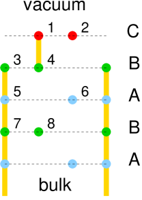
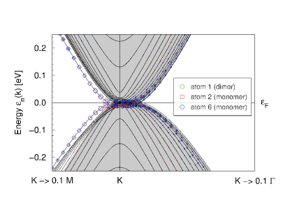
We have shown above that there are no surface bands in hexagonal graphite, but stacking faults can induce interface bands. The next issue is, if only one displaced surface layer with the geometry shown in Fig. 17 can do this job. The resulting band structure with band weights in Fig. 18 shows that at least on the line K - M there is a surface band which is mostly localized at the monomers 2 and 6 defined in Fig. 17. On the line K - there are surface resonances with increased weights toward the surface, but no real surface bands. Note that the structure has dimers at the surface which produce localized dimer bands (not shown) split by approximately 0.8 eV similar to the dimers near stacking faults. These dimer bands look very similar to those shown in the lower panel of Fig. 13 for a slab with stacking fault , but each dimer band is almost doubly degenerate with a slight splitting. This is due to the existence of two dimers in the unit cell of the slab (one on either surface) with a small interaction through the slab.
VI Summary
We investigated the electronic structure of hexagonal graphite without and with surfaces and stacking faults using self-consistent full-potential DFT calculations in the LDA and the GGA. There are two types of stacking faults (denoted by and ) which differ in the first place by their chemical bonding of the orbitals in the vicinity of the stacking fault (see Fig. 10). We find that
-
•
Pure surfaces do not host any surface bands in the energy range of the and bands. Because the LDOS around in the surface layer is reduced, we expect a reduced surface conductivity compared with the bulk. Both, at the surface and in the bulk, the LDOS around is one order of magnitude larger for the single atoms than for the chain atoms. Therefore, all low-energy electronic properties (like electric conductivity, low-temperature thermal conductivity and specific heat) are governed by hopping processes between the dangling -orbitals of the single atoms.
-
•
Even displacement of one single atomic layer at the surface, which is the germ for producing a stacking fault in the crystal growing process, can induce surface bands.
-
•
Both types of stacking faults induce interface bands around the K-point in the Brillouin zone. Correspondingly, the LDOS at the single atoms near a stacking fault is enhanced over the bulk value. In the case of type the enhancement factor is of the order of 10. This indicates a large 2D electronic conductivity along the stacking fault.
-
•
Stacking faults of type (AB)n(CA)n (denoted by ) are characterized by -bonded dimers, which produce a pair of dimer bands. They are split by about 0.8 eV at the K-point and could be probed by near-infrared spectroscopy. Within the LDA, their electronic part of the formation energy is smaller than for the alternative type (AB)n(CB)n-1C (denoted by ).
Our results indicate that it can be extremely misleading if experiments on real graphite samples (which have most likely numerous stacking faults) are compared with electronic structure calculations on ideal lattices. This applies in particular to transport measurements which are governed by the electronic structure around the Fermi energy.
Acknowledgements.
We are indebted to J. van den Brink, J. Venderbos, P. Esquinazi and M. Knupfer for helpful discussions. Financial support was provided by DFG Grant RI932/6-1.References
- Neto et al. (2009) A. H. C. Neto, F. Guinea, N. M. R. Peres, L. S. Novoselov, and A. K. Geim, Rev. Mod. Phys. 81, 109 (2009).
- Abergel et al. (2010) D. S. L. Abergel, V. Alpakov, J. Berashevich, K. Ziegler, and T. Chakraborty, Adv. Phys. 59, 261 (2010).
- Peres (2010) N. M. R. Peres, Rev. Mod. Phys. 82, 2673 (2010).
- Goerbig (2011) M. Goerbig, Rev. Mod. Phys. 83, 1193 (2011).
- Kempa et al. (2006) H. Kempa, P. Esquinazi, and Y. Kopelevich, Solid State Commun. 138, 118 (2006).
- Arovas and Guinea (2008) D. P. Arovas and F. Guinea, Phys. Rev. B 78, 245 416 (2008).
- Koshino and McCann (2013) M. Koshino and E. McCann, Phys. Rev. B 87, 45 420 (2013).
- Brandt et al. (1988) N. B. Brandt, S. M. Chudinov, and Y. G. Ponomarev, Semimetals, 1. Graphite and its Compounds (North Holland, 1988).
- Grueneis et al. (2008) A. Grueneis, C. Attaccalite, L.Wirtz, H. Shiozawa, R. Saito, T. Pichler, and A. Rubio, Phys. Rev. B 78, 205 425 (2008).
- Charlier et al. (1994) J.-C. Charlier, X. Gonze, and J.-P. Michenaud, Carbon 32, 289 (1994).
- Latil and Henrard (2006) S. Latil and L. Henrard, Phys. Rev. Lett. 97, 036803 (2006).
- Aoki and Amawashi (2007) M. Aoki and H. Amawashi, Solid State Commun. 142, 123 (2007).
- Min et al. (2007) H. Min, B. Sahu, S. K. Banerjee, and A. H. MacDonald, Phys. Rev. B 75, 155115 (2007).
- Zhang et al. (2010) F. Zhang, B. Sahu, H. Min, and A. H. MacDonald, Phys. Rev. B 82, 35 409 (2010).
- Xiao et al. (2011) R. Xiao, F. Tasnadi, K. Koepernik, J. W. F. Venderbos, M. Richter, and M. Taut, Phys. Rev. B 84, 165 404 (2011).
- (16) http://www.fplo.de/, version: 9.01-35-x86_64.
- Koepernik and Eschrig (1999) K. Koepernik and H. Eschrig, Phys. Rev. B 59, 1743 (1999).
- Perdew and Wang (1992) J. Perdew and Y. Wang, Phys. Rev. B 45, 13 244 (1992).
- Perdew et al. (1996) J. Perdew, K. Burke, and M. Ernzerhof, Phys. Rev. Lett. 77, 3 865 (1996).
- Ooi et al. (2006) N. Ooi, A. Rairkar, and J. B. Adams, Carbon 44, 231 (2006).
- Lehmann and Taut (1972) G. Lehmann and M. Taut, phys. stat. sol. (b) 54, 469 (1972).
- Lehmann and Taut (1973) G. Lehmann and M. Taut, phys. stat. sol. (b) 57, 815 (1973).
- Kelly (1981) B. T. Kelly, Physics of Graphite (Applied Science Publishers, 1981).
- Charlier et al. (1991) J.-C. Charlier, X. Gonze, and J.-P. Michenaud, Phys. Rev. B 43, 4579 (1991).
- Slonzewski and Weiss (1958) J. C. Slonzewski and P. R. Weiss, Phys. Rev. 109, 272 (1958).
- McClure (1957) J. W. McClure, Phys. Rev. 108, 612 (1957).
- Luk’yanchuk and Kopelevich (2004) I. A. Luk’yanchuk and Y. Kopelevich, Phys. Rev. Lett. 93, 166 402 (2004).
- Sugawara et al. (2006) K. Sugawara, T. Sato, S. Souma, T. Takahashi, and H. Suematsu, Phys. Rev. B 73, 45 124 (2006).
- Heine (1962) V. Heine, Proc. Phys. Soc. 81, 300 (1962).
- (30) Because the total energy differences between different stacking orders are exceptionally small, for the total energy calculations we used a refined real space integration mesh for the potential matrix elements. The default mesh produces noice in the 10-5 eV energy range, which overshadows the physical energies in this case. We increased the number of radial mesh points to 200 and used the densest implemented angular mesh with 602 points on the unit uphere for each radial shell.
- Grimme (2011) S. Grimme, Comp. Mol. Sci. 1, 211 (2011).
- Grimme (2006) S. Grimme, J. Comput. Chem. 27, 1 787 (2006).
- Tomanek et al. (1987) D. Tomanek, S. G. Louie, H. J. Mamin, D. W. Abraham, R. E. Thomson, E. Ganz, and J. Clarke, Phys. Rev. B 35, 7790 (1987).
- Boettger (1994) J. C. Boettger, Phys. Rev. B 49, 16 798 (1994).