Symmetry-Tunable Environment in Functional Ferroic Heterostructures
Abstract
We demonstrate a concept for post-growth symmetry control in oxide heterostructures. A functional oxide is sandwiched between two ferroelectric layers and inversion symmetry at the position of the oxide constituent is reversibly switched on or off by layer-selective electric-field poling. The functionality of this process is monitored by optical second harmonic generation. The generalization of our approach to other materials and symmetries is considered. We thus establish ferroic trilayer structures as device components in which symmetry-driven charge-, spin-, and strain-related functionalities can be activated and deactivated at will.
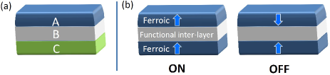
The correspondance of symmetry and functionality pervades all fields in physics and is a cornerstone for optimizing the performance of functional materials for technological applications Curie94 ; Livio12 ; Hwang12a . Symmetry violations in time and space, for instance, are a hallmark for the emergence of magnetic and electric long-range order, respectively. If both of these symmetries are broken novel interactions like magnetoelectric coupling effects are activated. A promising pathway towards enhanced or novel functionalities is to incorporate such symmetry violations directly into the material design. This becomes feasible when using high-end deposition techniques that allow for symmetry engineering at the atomic level by growing atomically sharp interfaces Hwang12a ; Mannhart10a . Growth-induced inversion symmetry violation, for example, can activate spin-orbit mediated phenomena such as spin-band splitting (Rashba effect Rashba60a ) or spin canting (Dzyaloshinskii-Moriya interaction Moriya60a ). This is a source for spin-polarized currents in thin-film semiconductors and ferromagnetic contributions in otherwise antiferromagnetic systems Koga02 ; Nitta97 ; Ederer05a ; Cheong07 . A particularly elegant way for generating the desired symmetry reduction is acquired in so-called tricolor superlattices where a geometric inversion symmetry breaking is achieved by the stacking three of constituents, A - B - C, as illustrated in Fig. 1(a) Sai00a ; Warusawithana03a . Here, as a consequence of the artificially lowered symmetry, an enhanced electric polarization Lee05a and interface magnetization Yamada04a , as well as unusual optical properties Zubko11a ; Figotin03a ; Lepri11a may arise. Unfortunately, a growth-based compositional symmetry breaking of the ABC-type is inevitably immutable: It cannot be altered after the completion of growth. In this sense, ABC-type heterostructures following the classical device paradigm may be regarded as passive building blocks. Here the step toward active heterostructures in which symmetry-driven functionalities can be repeatedly switched on and off via reversible post-growth symmetry control would be a major achievement.
In this work we report such reversible post-growth symmetry control using epitaxial trilayer heterostructures with controllable inversion-symmetry properties as model system. We sandwich a functional candidate compound between two ferroelectric layers and violate or restore the net inversion symmetry by controlling the associated polarization configuration as sketched in Fig. 1(b). The latter is readily accomplished with moderate voltages applied at room-temperature and monitored by optical second harmonic generation (SHG) as symmetry-sensitive detection tool.
For realizing symmetry-tunable heterostructures we selected the textbook ferroelectric PbZr0.2Ti0.8O3 (PZT) as constituent providing the symmetry environment and metallic La0.7Sr0.3MnO3 (LSMO) as functional inter-layer. Epitaxial PZT(001) (50 nm) /LSMO(001) (5 nm) /PZT(001) (50 nm) trilayers were grown on (001)-oriented SrTiO3 (STO) substrates by pulsed laser deposition (PLD). The PZT thickness was set to 50 nm in order to retain the epitaxial strain imposed by the substrate and thus maintain a ferroelectric single-domain state Nagarajan99a . Figure 2(a) shows a cross section of the PZT/LSMO/PZT trilayer system imaged by high-angle annular dark field (HAADF) scanning transmission electron microscopy (STEM). The image (Z-contrast) reveals high-quality interfaces without any evidence of inter-diffusion. Moreover, the direct visualization of the structure allows to determine the trilayer polarization state which manifests as a cation (Ti/Zr) off-centering along the [001] growth direction in the PZT unit cells. This offset is visible in Figs. 2(b) and (c), which show a blow-up of the structure in the upper and lower PZT layer of Fig. 2(a), respectively. Based on the observed Ti/Zr offset we conclude that the polarization alternates according to across the LSMO inter-layer with a sharp transition at the PZT/LSMO interfaces.
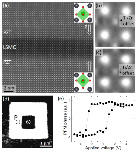
Piezoresponse force microscopy (PFM) was applied in order to unveil the two trilayer polarization states in the PZT/LSMO/PZT system illustrated in Fig. 1(b). We investigated the effect of applying an electric voltage of V to the top ferroelectric layer. Figure 2(d) shows the out-of-plane PFM contrast obtained after poling a box-in-box structure with the PFM tip. Bright and dark regions correspond to a ferroelectric single domain state with and , respectively, clearly indicating that the upper layer can be selectively and reversibly switched between two stable ferroelectric states. This constitutes the two symmetry environments illustrated in Fig. 1(b). The locally acquired hysteresis loop in the piezoelectric (resp. ferroelectric) response shown in Fig. 2(e) reflects the excellent ferroelectric performance of the switchable PZT control-layer. However, note that the negative bias of the local PFM loop in Fig. 2(e) indicates an influence on the PZT switching behavior exerted by the electrostatic environment or by interfacial strain Yu12a ; Vrejoiu08a . Thus, although the PFM data in Figs. 2(d) and (e) reveals the presence of two stables states for the upper ferroelectric PZT layer, we cannot yet exclude that the lower PZT layer is at least partially switched by the poling field.
For further verification of this issue we therefore devised an experiment that allows us to probe the trilayer net symmetry in a convenient non-invasive and non-destructive way. Based on the von-Neumann principle the gain and loss of inversion symmetry is expected to directly manifest in the physical properties of the trilayer system, including its optical response. In particular, optical frequency doubling — also known as second harmonic generation (SHG) — can, in the leading electric-dipole order, only occur when the trilayer inversion symmetry is broken Fiebig04a ; Denev11a . This is described by the relation
| (1) |
with the electric field of the incident light wave at frequency , the induced electric-dipole oscillation at frequency , and the effective nonlinear susceptibility tensor of the trilayer. For an antiparallel orientation of the polarization in the two PZT layers (OFF state in Fig. 1(b)) the systems inversion symmetry is not violated so that holds. In contrast, inversion symmetry is broken for parallel orientation of the polarization in the two PZT layers so that SHG is symmetry-allowed in this ON state (). In order to confirm that SHG indeed probes the entire trilayer net symmetry expressed by , we measured a model system that allows us to approach the geometry and symmetry of the full trilayer system step by step.
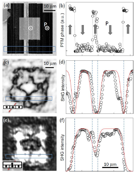
At first, PZT single layers with a thickness of 50 nm were grown on SrRuO3 (SRO) buffered (001)-oriented STO. As indicated by the PFM image in Fig. 3(a) the PZT grows in a ferroelectric single-domain state and can be reversibly switched by applying V to the PFM tip. In Figs. 3(c) to (f) we show the corresponding SHG analysis performed with a standard transmission setup described elsewhere Fiebig04a . In our experiments, light at a photon energy around 1.0 eV was incident at an angle of about 20∘ with respect to the surface normal of the PZT film. Because of the tilt, SHG components sensitive to the ferroelectric polarization along the [001] direction can be excited. A spatially resolved SHG measurement taken with SHG light from one of these components is presented in Fig. 3(c). The black lines in the image retrace the ferroelectric 180∘ domain walls of the electrically poled box-in-box structure. This is further highlighted in Figs. 3(b) and (d) which show the variation of the PFM and SHG contrast along cross-sections of the corresponding images. For modelling the lateral dependence of the SHG intensity we calculated the local interference of SHG contributions from neighboring domains with the spontaneous polarization and . Because of the linear coupling of the SHG susceptibility to the spontaneous polarization the sign reversal of is converted into a phase difference between SHG waves emitted from opposite domains Fiebig02a . Thus, the net SHG yield is given by
| (2) |
Here accounts for the domain distribution in Fig. 3(a) and m is entered as optical resolution. The good agreement between the SHG data and the calculated intensity profile in Fig. 3(d) corroborates that the SHG process is sensitive to the polarization state of the single 50 nm PZT layer investigated here.
Taking advantage of this sensitivity we then investigated the SHG response of an assembly that emulates the final symmetry-controlled ABA-type structures of Fig. 1(b) by a “trilayer construction kit”. This was built by mounting the switched PZT film of Fig. 3(a) on top of a single-domain PZT/SRO/STO heterostructure with the two PZT layers facing each other. Repeating the SHG experiments on this model trilayer we now obtained a pronounced contrast in the SHG image shown in Fig. 3(e). Because of the well-defined polarization state of the “trilayer construction kit” (see inset to Fig. 3(e)) the SHG brightness levels can be unambiguously assigned to the local symmetry state. We find that dark regions correspond to a centrosymmetric trilayer state, whereas bright regions are observed when inversion symmetry is broken Kaneshiro08a . The good agreement between the SHG data and the calculated intensity profile in Fig. 3(f) confirms that the SHG method is capable of probing the ferroelectric polarization state in buried layers expressed by the coupling to and hence the net symmetry of the entire arrangement.
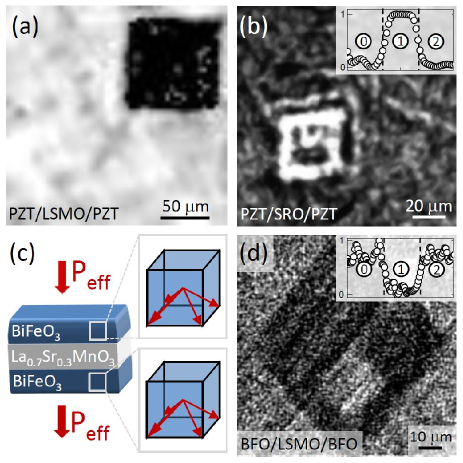
The empirical demonstration leads us to the final step: the SHG analysis of the real trilayer system, i.e. on the epitaxial PZT/LSMO/PZT trilayer grown on a SRO-buffered STO substrate. Figure 4(a) displays the corresponding spatially resolved SHG data taken after electrically poling an area of m2 with a PFM tip. The poled area (dark) shows a distinct contrast level and is clearly distinguished from the surrounding region (bright). Referring to Fig. 3(e) we can conclude that the pronounced SHG contrast indicates a polarization reversal in the top PZT layer, and along with it a symmetry change in the PZT/LSMO/PZT trilayer. In the present case the system has been switched from a non-centrosymmetic (white ON) to a centrosymmetric (black OFF) state. This switching behavior confirms that the top and bottom control layers are decoupled which is essential for manipulating the symmetry state at the position of the functional layer. In the present case the decoupling is supported by conduction in the LSMO inter-layer. The inter-layer, however, does not have to be conducting: the decoupling of the control layers may as well be acquired via bias effects as seen in Fig. 2(b) or by pinning the polarization of the lower control layer, e.g. by doping or an additional bottom electrode.
Note that the concept for active inversion symmetry control by ferroelectric poling is not restricted to the case of PZT/LSMO/PZT trilayers. As suggested by Fig. 1(b) it is a universal approach in the sense that no restrictions apply regarding the materials which are chosen as the functional inter-layer and the ferroelectric control-layers. In order to verify the general validity we realized different trilayer compositions by exchanging, in two separate variations, either the material used for (i) the functional inter-layer or (ii) the ferroelectric control-layers.
(i) We begin with a discussion of the effects observed when replacing LSMO for SRO. The PFM analysis on PLD grown high-quality PZT/SRO/PZT trilayers on STO (001) revealed that the top PZT layer grows in a ferroelectric mono-domain state and can be reversibly switched by applying a voltage of V to the PFM tip (not shown). In Fig. 4(b) we present the corresponding spatially resolved SHG data taken on a PZT/SRO/PZT trilayer (50 nm/25 nm/50 nm) after electrically poling a box-in-box structure. In the SHG image poled and unpoled areas are again clearly distinguishable due to pronounced SHG contrasts that, analogous to the case of LSMO, relate to the local symmetry state of the system (dark centrosymmetric, bright non-centrosymmetric). This evidences that the substitution of the inter-layer material has no fundamental influence on the basic trilayer performance of Fig. 1(b) so that we have the freedom to choose the inter-layer material according to the desired functionality.
(ii) In the next step we replaced the ferroelectric PZT control-layers by multiferroic BiFeO3 (BFO) films while keeping the initial LSMO inter-layer. In BFO the coexistence of electric and magnetic order simultaneously violates space- and time-reversal symmetry. Thus, the use of BFO as control-layer constituent allows us to exploit the electronic and the spin degrees of freedom in our symmetry-tunable trilayer environment. BFO/LSMO/BFO trilayers were grown on (001)-oriented STO substrates leading to four ferroelectric (multiferroic) in-plane variants with (see Fig. 4(c)) resulting from the cubic symmetry of the substrate Chu07a ; Yu12a . The associated domain sizes, however, are in the order of 10–100 nm. It is therefore sufficient to consider only the effective out-of-plane polarization component, , for analyzing the symmetry state that is seen by SHG and other mesoscopic probes with a limited resolution in the micrometer-regime. From previous work it is further known that is accompanied by a collinearly oriented small spontaneous magnetization Trassin13a , , which results from a canting in the antiferromagnetic spin arrangement of the BFO films Ederer05a . Thus, any reversal of coincides with a reorientation of which extends the symmetry control in our trilayers toward time reversal and the spin system.
PFM scans performed on a BFO/LSMO/BFO trilayer (50 nm/30 nm/50 nm) revealed a homogenous out-of-plane contrast for the upper BFO control-layer (see Fig. 4(c) for a schematic illustration). Figure 4(d) presents the corresponding SHG data taken after electrically poling a box-in-box structure with a PFM tip ( V). Similar to Fig. 4(a) a striking decrease in the SHG yield is observed when switching () in the upper BFO control-layer. It shows that the poling process establishes space- and time-reversal symmetry which, prior to the poling, have been broken in the BFO/LSMO/BFO system. A second electrical switch (inner box) then leads to full recovery of the initial signal strength which demonstrates that the symmetry violations in space and time are fully reversible.
In conclusion we demonstrated a concept for post-growth symmetry control in thin film heterostructures consisting of a functional constituent sandwiched between two ferroic control layers. As model case we discussed the activation and deactivation of a non-centrosymmetric environment that was achieved by selective voltage-driven switching in one out of two ferroelectric control layers. Subsequent experiments demonstrated the generality of the approach. It is robust against an exchange of the control as well as the functional layers. By involving multiferroic BFO we showed that even the type of environmental control is selectable. Aside from the spatial inversion exemplarily discussed in this work it may involve space-time reversal via multiferroic control layers (extending the classical spin-valve geometry Chappert07a ), or strain via ferroelastic control layers. Our concept thus reveals a universal route for gaining control of electric, magnetic, distortive, or even orbital degrees of freedom post-growth which is a basis for applications employing heterostructure as active device components in which tailored asymmetry-driven functionalities can be switched on and off at will.
M.T. acknowledges subsidy from the Center for Energy Efficient Electronics Science (NSF Grant No. 0939514). D.M. appreciates support by the Alexander von Humboldt Foundation. The authors thank J. Seidel, J. Heron, and J. Clarkson for experimental assistance.
References
- (1) P. Curie, Journal Phys. T. A. 3, 393 (1894).
- (2) M. Livio, Nature 490, 472 (2012).
- (3) H. Y. Hwang, Y. Iwasa, M. Kawasaki, B. Keimer, N. Nagaosa, and Y. Tokura, Nature Mater. 11, 103 (2012).
- (4) J. Mannhart and D. G. Schlom, Science 327, 1607 (2010).
- (5) E. I. Rashba, Sov. Phys. Solid State 2, 1109 (1960).
- (6) T. Moriya, Phys. Rev. 120, 91 (1960).
- (7) T. Koga, J. Nitta, and H. Takayanagi, Phys. Rev. Lett. 88, 126601 (2002).
- (8) J. Nitta, T. Akazaki, and H. Takayanagi, Phys. Rev. Lett. 78, 1335 (1997).
- (9) C. Ederer and N. A. Spaldin, Phys. Rev. B 71, 060401(R) (2005).
- (10) S. W. Cheong and M. Mostovoy, Nature Mater. 6, 13 (2007).
- (11) N. Sai, B. Meyer, and D. Vanderbilt, Phys. Rev. Lett. 84, 5636 (2000).
- (12) M. P. Warusawithana, E. V. Colla, J. N. Eckstein, and M. B. Weissman, Phys. Rev. Lett. 90, 036802 (2003).
- (13) H. N. Lee, H. M. Christen, M. F. Chrisholm, C. M. Rouleau, and D. H. Lowndes, Nature 433, 395 (2005).
- (14) H. Yamada, Y. Ogawa, Y. Ishii, H. Sato, M. Kawasaki, H. Akoh, and Y. Tokura, Science 305, 646 (2004).
- (15) P. Zubko, S. Garliglio, M. Gagay, P. Ghosez, and J.-M. Triscone, Annu. Rev. Cond. Mat. Phys. 2, 141 (2011).
- (16) A. Figotin and I. Vitebskiy, Phys. Rev. B 67, 16 (2003).
- (17) S. Lepri and G. Casati, Phys. Rev. Lett. 106, 164101 (2000).
- (18) V. Nagarajan, I. G. Jenkins, S. P. Alpay, H. Li, S. Aggarwal, L. Salamanca-Riba, A. L. Roytburd, and R. Ramesh, J. Appl. Phys. 86, 595 (1999).
- (19) P. Yu, W. Luo, D. Yi, J. X. Zhang, M. D. Rossell, C.-H. Yang, L. You, G. Singh-Bhalla, S. Y. Yang, Q. He, Q. M. Ramasse, R. Erni, L. W. Martin, Y. H. Chu, S. T. Pantelides, S. J. Pennycook, and R. Ramesh, PNAS 109, 9710 (2012).
- (20) I. Vrejoiu, M. Ziese, A. Setzer, P. D. Esquinazi, B. I. Birajdar, A. Lotnyk, M. Alexe, and D. Hesse, Appl. Phys. Lett. 92, 152506 (2008).
- (21) M. Fiebig and R. Pisarev, J. Magn. Magn. Mater. 272, 1607 (2004).
- (22) S. A. Denev, T. T. A. Lummen, E. Barnes, A. Kumar, and V. Gopalan, J. Am. Ceram. Soc. 94, 2699 (2011).
- (23) M. Fiebig, D. Fröhlich, T. Lottermoser, and M. Maat, Phys. Rev. B 66, 144102 (2002).
- (24) J. Kaneshiro, S. Kawado, H. Yokota, Y. Uesu, and T. Fukui, J. Appl. Phys. 104, 054112 (2008).
- (25) Y.-H. Chu, M. P. Cruz, C.-H. Yang, L. W. Martin, P.-L. Yang, J.-X. Zhang, K. Lee, P. Yu, L.-Q. Chen, and R. Ramesh, Adv. Mater. 19, 2662 (2007).
- (26) M. Trassin, J. D. Clarkson, S. R. Bowden, J. Liu, J. T. Heron, R. J. Paull, E. Arenholz, D. T. Pierce, and J. Unguris, Phys. Rev. B 87, 134426 (2013).
- (27) C. Chappert, A. Fert, and F. Nguyen Van Dau, Nature Mater. 6, 813 (2007).