First-principles study of the thermoelectric properties of strained graphene nanoribbons
Abstract
We study the transport properties, in particular, the thermoelectric figure of merit () of armchair graphene nanoribbons, AGNR- (for , with widths ranging from to Å) through strain engineering, where is the number of carbon dimer lines across the AGNR width. We find that the tensile strain applied to AGNR- changes the transport properties by modifying the electronic structures and phonon dispersion relations. The tensile strain increases the value of the AGNR- families with and , where is an integer. Our analysis based on accurate density-functional theory calculations suggests a possible route to increase the values of AGNR- for potential thermoelectric applications.
I Introduction
Currently thermoelectric materials receive considerable attentionSzczech et al. (2011) due to their ability to produce electricity from waste heat generated in, for example, power plants and refrigeration units. The efficiency of a thermoelectric material is characterized by the figure of merit
where is the electrical conductance, is the Seebeck coefficient, () is the thermal conductance due to electrons (phonons), and is the absolute temperature. It is challenging to engineer thermoelectric materials because the parameters , , , and are intricately interrelated; an attempt to improve one parameter usually detrimentally affects the others.Snyder and Toberer (2008) It is generally agreed that for thermoelectric generators to be viable, a material with is required.Sootsman et al. (2009); Tritt (2011)
Current state-of-the-art thermoelectric materialsTritt (2011); Teweldebrhan et al. (2010a); Goyal et al. (2010); Teweldebrhan et al. (2010b) such as single-layer Bi2Te3 and AgPb18SbTe20 possess between and , but they are composed of high atomic number elements, thus making them both expensive and heavy. Graphene, which is composed of a hexagonal network of lightweight carbon atoms, with extremely high electron mobility and long electron mean free paths,Bolotin et al. (2008a) is a potential thermoelectric material. Experimental measurements of for graphene showed values of VK-1 at K,Zuev et al. (2009) VK-1 at K,Wei et al. (2009) and VK-1 at K,Checkelsky and Ong (2009) which are moderate compared to VK-1 at room temperature for the inorganic materials,Harman et al. (2002); Hsu et al. (2004); Ohta et al. (2007) but comparable to other organic thermoelectric materials such as conducting polymers.Dubey and Leclerc (2011)
Since graphene has very high ,Balandin et al. (2008); Faugeras et al. (2010); Balandin (2011); Nika and Balandin (2012) a common approach to increase of graphene-related materials is to reduce . For example, edge disorder decreases the phonon mean free path and therefore reduces , which may increase . However, edge disorder impacts the electronic structure of the materials as well. In the case of armchair graphene nanoribbons (GNRs), Ouyang and Guo (2009); Mazzamuto et al. (2012) edge disorder turns out to be detrimental to ; whereas for zigzag graphene nanoribbons, a high was obtained.Sevinçli and Cuniberti (2010)
Introducing vacancies into GNRs may also reduce phonon thermal conductance. Randomly distributed vacancies tend to decrease ,Ouyang and Guo (2009); Mazzamuto et al. (2012) while periodically distributed lattice defects increases . The maximal attainableGunst et al. (2011); Zhao et al. (2011a) is to .
Other methods to suppress involves crafting graphene into novel nanostructures. Graphene nanojunctions, which consist of graphene domains with different widths connected together,Chen et al. (2010) demonstrated a maximum . In a similar vein, attaching “stub” structures to the edges of GNRsXie et al. (2012) resulted in . In the case of kinked GNRs, a maximum can be achieved.Huang et al. (2011) Cutting graphene into “nanowiggles”Liang et al. (2012) delivered a maximum , while crafting graphene into structures with alternating armchair-edge and zigzag-edge domainsMazzamuto et al. (2011) delivered .
There have also been attempts to combine the two methods above by etching periodic vacancies into novel graphene nanostructures. A maximum of and even have been reported in these structures.Mazzamuto et al. (2012); Chang and Nikolić (2012)
Finally, the thermoelectric properties of graphene may be improved by incorporating heteroatomsNi et al. (2009); Yang et al. (2012) or isotopesChen et al. (2012); Balandin and Nika (2012) into it. For example, by attaching hydrogen atoms on the surface of the GNRs, was reported.Ni et al. (2009) The thermoelectric properties of hybrid nanoribbons consisting of alternating graphene and hexagonal boron nitride regions have also been investigated.Yang et al. (2012) A maximum was observed.
The strategies mentioned above face several challenges as they involve engineering complex shapes out of GNRs. Furthermore, foreign entities incorporated into graphene are either removed,Elias et al. (2009) or nucleate to form large clusters,Ci et al. (2010) when subjected to elevated temperatures. Inspired by previous works that showed that tensile strain reduces the of graphene-related materials,Zhai and Jin (2011); Wei et al. (2011); Yeo et al. (2012) we examine the effect of strain on the value of armchair graphene nanoribbons (AGNRs). Compared to the methods mentioned above, tensile strainLu et al. (2012) is relatively easier to be imposed on AGNRs, thus enabling a possible route to manipulate the values.
II Methodology
To calculate the thermoelectric properties of the AGNR- with a strain parameter , we use the Landauer approach to calculate the transport properties, where the electrical conductance , the Seebeck coefficient , and the thermal conductance due to electrons are obtained in the linear response regime under an open circuit condition:
| (1) |
| (2) |
| (3) |
where the th order Lorenz function is given by
| (4) |
In the above equations, is the elementary charge, is the Fermi-Dirac distribution with energy , chemical potential , and temperature . The Planck and Boltzmann constants are and , respectively. is the electronic transmission function, which is the number of effective modes available for electronic transport at . We expect Eq. 1 to Eq. 4 to be valid even for the case of one-atom thick AGNRs since the approximations made to derive them do not take the dimensionality of the system into account. Assuming ballistic transport (since our system sizes are much smaller than the typical electronBolotin et al. (2008b) and phononGhosh et al. (2008) mean free paths) and completely uniform contact and transport regions, we can calculate by counting the number of bands at from the electronic band structure along the transport direction of interest.Markussen et al. (2008); Jeong et al. (2010) We note here that for more general cases, may be calculated using the nonequilibrium Green’s function method.Wang et al. (2013) Since the highest doping concentration achievableLee et al. (2010) so far by molecular charge-transfer and hetero-atom doping of graphene is cm-2, we investigate doping concentrations in AGNR- from to cm-2; with a negative (positive) concentration representing electron or n-type doping (hole or p-type doping). We consider both n- and p-type doping because thermoelectric devices requires both types of materials. We restrict our study to temperatures from to K.
We perform nonspin-polarized density-functional theory (DFT) calculations on AGNRs using the SIESTA package.Soler et al. (2002) The unit cell of AGNR- is shown in Figure 1, where is the number of carbon dimer lines across the AGNR, and each carbon atom at the edge is terminated with a single hydrogen atom. A vacuum separation of at least 15 Å is imposed in the and directions, where we use the convention adopted in Figure1. The local density approximation (LDA) is used for the exchange–correlation functional. Troullier–Martins pseudopotentials and double- basis sets are used for the carbon and hydrogen atoms. A mesh cutoff of 400 Ryd is used. We obtain the optimized length of each in the direction (i.e., the transport direction) by relaxing the atomic positions of AGNR- with different ribbon lengths . The atomic relaxation is performed using the conjugate gradient algorithm with a force tolerance criterion of eV/Å. The total energies of the relaxed structures are fitted to a polynomial function as a function of to obtain . For the strained AGNRs, we use unit cells with , with different strain parameter values of , , , and . We note that AGNRs have compressive edge stresses that tend to cause them to buckle.Gan and Srolovitz (2010); Bao et al. (2009); Kumar et al. (2010) Since a large unit cell of a buckled AGNR imposes a huge computational demand on accurate DFT calculations, we consider the AGNRs under tensile strain in this study.

The thermal conductance due to lattice vibrations is calculated according to
where is the Bose-Einstein distribution with frequency , and is the phonon transmission function obtained using the counting method on the phonon dispersion relations. The supercell force-constant method is used to perform the phonon calculations.Yeo et al. (2012); Gan et al. (2006); Zhao et al. (2011b)
III Results and Discussion
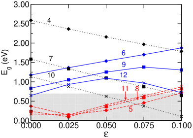
We first examine the effect of tensile strain on the electronic band structures of the AGNR-. The electronic band gap has a very important influence on the thermoelectric behavior of materials: we need an of at least to to prevent bipolar transport because concurrent electron and hole transport leads to an opposing effect that reduces the Seebeck coefficient. Figure 2 shows the band gap of the AGNRs as a function of . It is well-known that the use of the local density approximation for the exchange-correlation functional underestimates , but we expect the correct overall qualitative trends to be obtained.Yang et al. (2007) In our calculations using LDA, ranges from eV for AGNR- to eV for AGNR-. In comparison, with GW calculations, varies from eV for AGNR- to eV for AGNR-.Yang et al. (2007) The of AGNR- for depends on through a 3-family behavior: , where is an integer.Son et al. (2006) Figure 2 shows how varies with for different families. For the family with the largest , , decreases linearly with . For the family of , increases with except for large for and . For the family of , generally increases with for all , except at . The maximum percentage change to for is substantial as it ranges from % in AGNR- to % in AGNR-. For much wider AGNRs (), a previous studySun et al. (2008) noted that shows a zigzag fluctuation with . This suggests that it is much harder to tune by modifying for large .
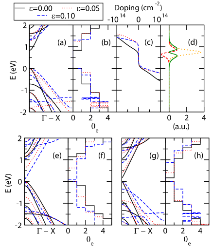
The Lorenz functions in Eq. 4 for the evaluation of , , and depend critically on the location of and the extent (or spread) of , both of which are controlled by the doping concentration and temperature. The values of for AGNR- as a function of doping concentration for different are shown in Figure 3(c). The spread of spans only around (see Figure 3(d)), and thus severely restricts the range of for the integration of . As a reference, we note that at K, corresponds to eV. We shall therefore study the changes of around the conduction (valence) band edge induced by for n-type (p-type) doping to obtain a qualitative understanding of the variations of , , and as a result of and temperature.
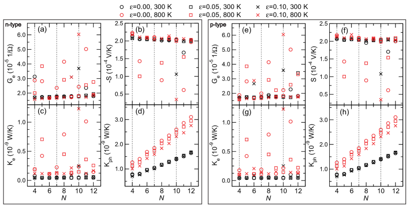
Figure 3(a, e, g) shows the electronic band structures, and 3(b, f, h) the of the representative AGNR- from each family, , , and . From Figure 3(a), we observe that AGNR- from the family displays an increase in near the band edges for non-zero . From Figure 3(f), AGNR- (a member of the family) shows a decrease in around the band edges. Finally, members of the family display very little changes in to within eV (the range at which is nonzero at K) around the band edges with increasing ; this is shown in Figure 3(h) for AGNR-.
We plot the various transport parameters for the determination of for n- and p-type doping in Figure 4 at and K with corresponding values of and eV, respectively. At a moderate temperature such as K, the transport is governed by monopolar transport, where the values of , , and vary only slightly with changes with . Physically this means electronic excitation is limited at this temperature. The only exception is AGNR- at , where its is so small compared to that bipolar transport governs and causes drastic changes in , , and . At a high temperature K, we expect AGNR- with eV to be affected by bipolar transport, where and will generally increase due to the presence of both types of carriers (i.e., electrons and holes) for charge and heat transport, but will decrease due to the opposing effect we mentioned earlier. This is generally evident in Figure 4 where the values of , , and change drastically at K compared to that for K for all strain values, as long as eV.
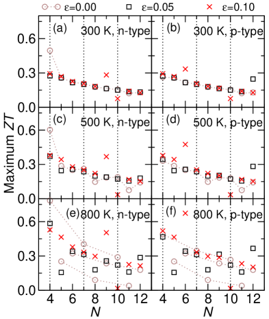
We shall give a detailed discussion of the effect of strain on AGNR-, first with , then , and finally . Particular attention will be paid to the variation in comparison with as well as the changes in the due to in determining the values of , , , , and finally . Unless otherwise stated, the temperature is taken to be K for the discussion. For AGNR- with , and values decrease with increasing for and (due mainly to the reduction in ), but and increase with increasing due to bipolar transport for . For , it remains essentially constant for and , but it decreases for . We note that remains essentially constant for and since it is proportional to , so the changes in is somewhat suppressed when the ratio is taken. The net outcome for changes in , , and , is shown in Fig. 5(e) where the value for AGNR- decreases with increasing .
Next we discuss the family, where and of AGNRs in the family generally increases with increasing . The increase in causes , , and to increase with . However, an increase in does not significantly benefit because even the smallest at for all AGNR- is already large enough to prevent bipolar transport. Overall, at K, the increase in both and causes to increase with strain (see Fig. 5(e)).
Since AGNR- have the smallest among the three families, therefore bipolar transport is present even at that benefits and but not . At K, bipolar transport becomes dominant and causes to become small. As increases with increasing , and decrease but increases since the monopolar transport becomes more pronounced. The overall effect, however, is to increase as shown in Fig. 5(e).
We now examine the effect of and temperature on and its associated influence on of AGNRs. The effect of temperature is also seen (see Fig. 4(d)) to increase the thermal conductance due to phonon () from K to K. However, at high temperatures, the effect of strain on for various could decrease the due an overall shifting down of the phonon frequencies as a result of weaker interatomic interactions.Yeo et al. (2012) For example, at K, a strain of could decrease by from that of the unstrained AGNRs. We note that the total thermal conductance of AGNRs is dominated by and not .
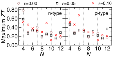
Figure 5 shows the maximum values attainable at , , and K for n- and p-type doping. It can be seen that at higher temperatures, changes more sensitively with because the larger spread of magnifies the changes to and due to . In general the value decreases with increasing due to the faster increase in as the AGNR- become wider. We observe that, under strain, increases for AGNR- belonging to the and families, but decreases for the family. It is interesting to note that at K and , bipolar transport becomes significant for AGNRs with small such that the monotonic decrease in values can be grouped according to three families, which is largely due to the 3-family behaviorSon et al. (2006) exhibited by .
Figure 6 shows the maximum value attainable for AGNR- in the temperature range K and doping concentration of to cm-2, giving an upper limit to the value that can be achieved through strain engineering. At the highest , increases by % for AGNRs in the family, and increases by % for the family. However, decreases by % for the family.
IV Conclusion
We have calculated the thermoelectric figure of merit for AGNR- ( is the number of carbon dimer lines across the AGNR width) when uniaxial tensile strain is applied along the main ribbon axis of the AGNR. We have considered both n- and p-type doping concentrations of up to cm-2 and a temperature range of K. Using density-functional theory calculations, the effect of is found to improve for AGNR-, for and . For the family, this is due to an increase in the electronic transmission around the valence and conduction band edges. For the family, it is due to an increase in the band gap that reduces the unfavorable bipolar transport. Based on first principles, we concluded that strain engineering provides a possible route to improve the values of two families of AGNR-.
Acknowledgements
We gratefully acknowledge the support of A*STAR Computational Resource Center (A*CRC) of Singapore.
References
- Szczech et al. (2011) J. R. Szczech, J. M. Higgins, and S. Jin, J. Mater. Chem. 21, 4037 (2011).
- Snyder and Toberer (2008) G. J. Snyder and E. S. Toberer, Nat. Mater. 7, 105 (2008).
- Sootsman et al. (2009) J. R. Sootsman, D. Y. Chung, and M. G. Kanatzidis, Angewandte Chemie International Edition 48, 8616 (2009).
- Tritt (2011) T. M. Tritt, Annu. Rev. Mater. Res. 41, 433 (2011).
- Teweldebrhan et al. (2010a) D. Teweldebrhan, V. Goyal, M. Rahman, and A. A. Balandin, Applied Physics Letters 96, 053107 (2010a), ISSN 00036951.
- Goyal et al. (2010) V. Goyal, D. Teweldebrhan, and A. A. Balandin, Applied Physics Letters 97, 133117 (2010), ISSN 00036951.
- Teweldebrhan et al. (2010b) D. Teweldebrhan, V. Goyal, and A. A. Balandin, Nano Letters 10, 1209 (2010b), ISSN 1530-6984.
- Bolotin et al. (2008a) K. I. Bolotin, K. J. Sikes, J. Hone, H. L. Stormer, and P. Kim, Phys. Rev. Lett. 101, 096802 (2008a).
- Zuev et al. (2009) Y. M. Zuev, W. Chang, and P. Kim, Phys. Rev. Lett. 102, 096807 (2009).
- Wei et al. (2009) P. Wei, W. Bao, Y. Pu, C. N. Lau, and J. Shi, Phys. Rev. Lett. 102, 166808 (2009).
- Checkelsky and Ong (2009) J. G. Checkelsky and N. P. Ong, Phys. Rev. B 80, 081413 (2009).
- Harman et al. (2002) T. C. Harman, P. J. Taylor, M. P. Walsh, and B. E. LaForge, Science 297, 2229 (2002).
- Hsu et al. (2004) K. F. Hsu, S. Loo, F. Guo, W. Chen, J. S. Dyck, C. Uher, T. Hogan, E. K. Polychroniadis, and M. G. Kanatzidis, Science 303, 818 (2004).
- Ohta et al. (2007) H. Ohta, S. Kim, Y. Mune, T. Mizoguchi, K. Nomura, S. Ohta, T. Nomura, Y. Nakanishi, Y. Ikuhara, M. Hirano, et al., Nature Mater. 6, 129 (2007).
- Dubey and Leclerc (2011) N. Dubey and M. Leclerc, J. Polym. Sci., Part B: Polym. Phys. 49, 467 (2011).
- Balandin et al. (2008) A. A. Balandin, S. Ghosh, W. Bao, I. Calizo, D. Teweldebrhan, F. Miao, and C. N. Lau, Nano Lett. 8, 902 (2008).
- Faugeras et al. (2010) C. Faugeras, B. Faugeras, M. Orlita, M. Potemski, R. R. Nair, and A. K. Geim, ACS Nano 4, 1889 (2010).
- Balandin (2011) A. A. Balandin, Nature Mater. 10, 569 (2011).
- Nika and Balandin (2012) D. L. Nika and A. A. Balandin, Journal of Physics: Condensed Matter 24, 233203 (2012), ISSN 0953-8984.
- Ouyang and Guo (2009) Y. Ouyang and J. Guo, Appl. Phys. Lett. 94, 263107 (2009).
- Mazzamuto et al. (2012) F. Mazzamuto, J. Saint-Martin, V. H. Nguyen, C. Chassat, and P. Dollfus, J. Comput. Chem. Electron. 11, 67 (2012).
- Sevinçli and Cuniberti (2010) H. Sevinçli and G. Cuniberti, Phys. Rev. B 81, 113401 (2010).
- Gunst et al. (2011) T. Gunst, T. Markussen, A. -P. Jauho, and M. Brandbyge, Phys. Rev. B 84, 155449 (2011).
- Zhao et al. (2011a) W. Zhao, Z. X. Guo, J. X. Cao, and J. W. Ding, AIP Advances 1, 042135 (2011a).
- Chen et al. (2010) Y. Chen, T. Jayasekera, A. Calzolari, K. W. Kim, and M. Buongiorno Nardelli, J. Phys.: Condens. Matter 22, 372202 (2010).
- Xie et al. (2012) Z.-X. Xie, L.-M. Tang, C.-N. Pan, K.-M. Li, K.-Q. Chen, and W. Duan, Appl. Phys. Lett. 100, 073105 (2012).
- Huang et al. (2011) W. Huang, J.-S. Wang, and G. Liang, Phys. Rev. B 84, 045410 (2011).
- Liang et al. (2012) L. Liang, E. Cruz-Silva, E. C. Girão, and V. Meunier, Phys. Rev. B 86, 115438 (2012).
- Mazzamuto et al. (2011) F. Mazzamuto, V. Hung Nguyen, Y. Apertet, C. Caër, C. Chassat, J. Saint-Martin, and P. Dollfus, Phys. Rev. B 83, 235426 (2011).
- Chang and Nikolić (2012) P.-H. Chang and B. K. Nikolić, Phys. Rev. B 86, 041406 (2012).
- Ni et al. (2009) X. Ni, G. Liang, J.-S. Wang, and B. Li, Appl. Phys. Lett. 95, 192114 (2009).
- Yang et al. (2012) K. Yang, Y. Chen, R. D’Agosta, Y. Xie, J. Zhong, and A. Rubio, Phys. Rev. B 86, 045425 (2012).
- Chen et al. (2012) S. Chen, Q. Wu, C. Mishra, J. Kang, H. Zhang, K. Cho, W. Cai, A. A. Balandin, and R. S. Ruoff, Nature Materials 11, 203 (2012), ISSN 1476-1122.
- Balandin and Nika (2012) A. A. Balandin and D. L. Nika, Materials Today 15, 266 (2012), ISSN 1369-7021.
- Elias et al. (2009) D. C. Elias, R. R. Nair, T. M. G. Mohiuddin, S. V. Morozov, P. Blake, M. P. Halsall, A. C. Ferrari, D. W. Boukhvalov, M. I. Katsnelson, A. K. Geim, et al., Science 323, 610 (2009).
- Ci et al. (2010) L. Ci, L. Song, C. Jin, D. Jariwala, D. Wu, Y. Li, A. Srivastava, Z. F. Wang, K. Storr, L. Balicas, et al., Nat. Mater. 9, 430 (2010).
- Zhai and Jin (2011) X. Zhai and G. Jin, EPL (Europhysics Letters) 96, 16002 (2011).
- Wei et al. (2011) N. Wei, L. Xu, H. Q. Wang, and J. C. Zheng, Nanotechnology 22, 105705 (2011).
- Yeo et al. (2012) P. S. E. Yeo, K. P. Loh, and C. K. Gan, Nanotechnology 23, 495702 (2012).
- Lu et al. (2012) T.-Y. Lu, X.-X. Liao, H.-Q. Wang, and J.-C. Zheng, J. Mater. Chem. 22, 10062 (2012).
- Bolotin et al. (2008b) K. I. Bolotin, K. J. Sikes, Z. Jiang, M. Klima, G. Fudenberg, J. Hone, P. Kim, and H. L. Stormer, Solid State Commun. 146, 351 (2008b).
- Ghosh et al. (2008) S. Ghosh, I. Calizo, D. Teweldebrhan, E. P. Pokatilov, D. L. Nika, A. A. Balandin, W. Bao, F. Miao, and C. N. Lau, Appl. Phys. Lett. 92, 151911 (2008).
- Markussen et al. (2008) T. Markussen, A. -P. Jauho, and M. Brandbyge, Nano Lett. 8, 3771 (2008).
- Jeong et al. (2010) C. Jeong, R. Kim, M. Luisier, S. Datta, and M. Lundstrom, J. Appl. Phys. 107, 023707 (2010).
- Wang et al. (2013) J.-S. Wang, B. K. Agarwalla, H. Li, and J. Thingna, Frontiers of Physics p. 1 (2013).
- Lee et al. (2010) B. Lee, Y. Chen, F. Duerr, D. Mastrogiovanni, E. Garfunkel, E. Y. Andrei, and V. Podzorov, Nano Lett. 10, 2427 (2010).
- Soler et al. (2002) J. Soler, E. Artacho, J. D. Gale, A. García, J. Junquera, P. Ordejón, and D. Sánchez-Portal, J. Phys.: Condens. Matter 14, 2745 (2002).
- Gan and Srolovitz (2010) C. K. Gan and D. J. Srolovitz, Phys. Rev. B 81, 125445 (2010).
- Bao et al. (2009) W. Bao, F. Miao, Z. Chen, H. Zhang, W. Jang, C. Dames, and C. N. Lau, Nature Nanotech. 4, 562 (2009).
- Kumar et al. (2010) S. Kumar, K. P. S. S. Hembram, and U. V. Waghmare, Phys. Rev. B 82, 115411 (2010).
- Gan et al. (2006) C. K. Gan, Y. P. Feng, and D. J. Srolovitz, Phys. Rev. B 73, 235214 (2006).
- Zhao et al. (2011b) Y. Y. Zhao, K. T. E. Chua, C. K. Gan, J. Zhang, B. Peng, Z. P. Peng, and Q. H. Xiong, Phys. Rev. B 84, 205330 (2011b).
- Yang et al. (2007) L. Yang, C.-H. Park, Y.-W. Son, M. L. Cohen, and S. G. Louie, Physical Review Letters 99, 186801 (2007).
- Son et al. (2006) Y. W. Son, M. L. Cohen, and S. G. Louie, Phys. Rev. Lett. 97, 216803 (2006).
- Sun et al. (2008) L. Sun, Q. Li, H. Ren, H. Su, Q. W. Shi, and J. Yang, J. Chem. Phys. 129, 074704 (2008).