Theoretical expectation of large Seebeck effect in PtAs2 and PtP2
Abstract
Motivated by a recent observation of good thermoelectric properties in PtSb2, we theoretically study related pyrites in an attempt to seek for a material which overcomes the suppression of the Seebeck coefficient at high temperatures.We find that PtAs2 and PtP2 are good candidates, where a larger band gap than in PtSb2 combined with the overall flatness of the band top gives rise to a monotonically increasing Seebeck coefficient up to high temperatures. This expectation has been confirmed quite recently for hole doped PtAs2, where a very large power factor of 65W/cmK2 at K is observed.
pacs:
Searching good thermoelectric materials is an challenging issue both from the viewpoint of fundamental physics and device applications. From the latter viewpoint in particular, the efficiency of thermoelectric materials is characterized by a dimensionless figure of merit, with , where is the power factor, , , and are the temperature, the Seebeck coefficient, the electric conductivity, and the thermal conductivity, respectivelyMahanrev . A large power factor requires simultaneously large and , but usually materials with large Seebeck coefficient have small conductivity. As a general way to overcome this problem, one of the present authors along with Arita proposed that a band shape that has a flat portion at the top (or the bottom), connected to a dispersive portion, can give rise to large conductivity and Seebeck coefficient simultaneously. This band shape is referred to as the pudding-mold type, and the theory was applied to NaxCoO2, a thermoelectric material with large metallic conductivity and power factor, discovered by Terasaki et alTerasaki .
Quite recently, Nishikubo et al. found that doping holes into a cubic pyrite material PtSb2 (Fig.1(a)) by partially substituting Pt by Ir as Pt1-xIrxSb2 gives rise to a metallic conductivity, while exhibiting a large Seebeck effect below room temperature, thereby resulting in a large power factor of 40W/cmK2 for Nishikubo . Referring to the band structure calculation in ref.Emtage , a possible relevance of the peculiar band structure has been pointed out. Succeedingly, we have analyzed the origin of this large Seebeck effect in PtSb2, and concluded that a fairly flat band with dispersive portions, which we called the “corrugated flat band”, plays an important roleMori . In the study, we also found that the narrowness of the valence-conduction band gap results in a reduction of the Seebeck coefficient at high temperatures. We analyzed how the band gap is determined from a tightbinding viewpoint, and concluded that if we could increase the hopping integral between Pt and Sb orbitals, the band gap increases, and the Seebeck coefficient monotonically increases up to high temperatures.
In the present study, we theoretically search for related pyrite materials that can give a larger band gap and hence a monotonically increasing Seebeck coefficient at high temperatures. We perform first principles band calculation for with Ni, Pd, Pt and P, As, Sb, which shows that the band gap for PtAs2 and PtP2 is large compared to that of PtSb2. By constructing a tightbinding model for the bands near the Fermi level exploiting maximally localized Wannier orbitals, it is found that the large band gap is indeed due to the large - hopping. Calculating the Seebeck coefficient using the obtained tightbinding model, we find a monotonically increasing large Seebeck coefficient against temperature for these two materials. For PtP2, we find an ideal band shape in the conduction band structure, so that better thermoelectric properties are expected in the electron doped regime.
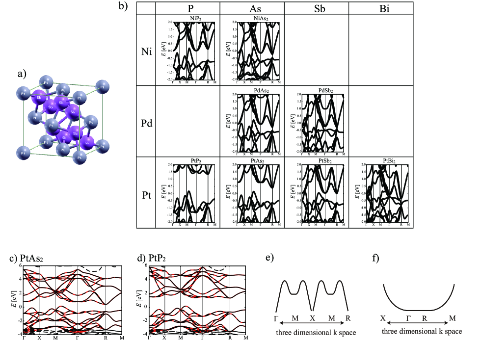
We start with the first principles band calculation for cubic pyrites with Pt, Pd, Ni and Sb, As, P. We adopt the lattice structure parameter values taken from ref.structure , and the band structure is calculated using the Wien2K packageWien2k . Here we take , 512 -points. The results are summarized in Fig.1(b). It can be seen that in PtAs2 and PtP2, a large band gap opens, while in other materials the gap is narrow or absent.
To see the origin of this result in more detail, we obtain tightbinding models exploiting the maximally localized Wannier orbitalsWannier . The bands near the Fermi level consist mainly of the orbitals, but in order to see the - hybridization explicitly, we first construct a 44 orbital - model that considers 20 (5 orbitals 4 sites) Mn orbitals in addition to the 24 Pn orbitals. The parameters listed in table 1 are the lattice constant, the largest hopping integral between and orbitals, the level offset between and orbitals, and the band gap . As analyzed in our previous studyMori , the band gap opens between the non-bonding (valence bands) and the antibonding bands (conduction bands), where non-bonding means that the band is almost solely constructed from orbitals. Therefore, the magnitude of the band gap should roughly be proportional to in the large limit.
| NiP2 | NiAs2 | PdAs2 | PdSb2 | PtP2 | PtAs2 | PtSb2 | PtBi2 | |
|---|---|---|---|---|---|---|---|---|
| 0.85 | 0.89 | 0.93 | 1.00 | 0.88 | 0.93 | 1.00 | 1.04 | |
| 0.41 | 0.33 | 1.33 | 1.45 | 0.63 | 0.76 | 1.00 | 1.08 | |
| 0.81 | 0.72 | 0.97 | 0.86 | 1.22 | 1.13 | 1.00 | 0.88 | |
| 0.96 | 0.87 | 0.86 | 0.69 | 1.46 | 1.27 | 1.00 | 0.81 |
There are two competing effects that affect the magnitude of ; one is the unit cell volume (the lattice constant) and the other is the spread of the or orbitals. When Sb is replaced by As or P, the unit cell volume and the orbital spread are both reduced, but the former effect overcomes the latter, thereby resulting in an enhanced . On the other hand, when Pt is replaced by Pd or Ni, the lattice contant barely changes, while the orbital shrinks, giving a smaller .
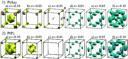
Having seen that the band gap of PtAs2 and PtP2 is large compared to that of PtSb2, we now analyze these two materials in more detail. To reproduce the band structure near the Fermi level, a 24 orbital model that considers only the Wannier orbitals (eight Pn per unit cell three orbitals) suffices. The band dispersion of the model is shown in fig.1(c) and (d) superposed to the original first principles band. The Fermi surface of the two materials is obtained using these models for several hole or electron doping rates as shown in Fig.2. In the hole doped case, it can be seen that the Fermi surface pockets are scattered through the entire Brillouin zone except around the and X points, indicating that the valence band is essentially flat (i.e. have similar energies) over a large portion of the zone with some corrugation. This can be seen in the band structure in Fig.1(c), in which the top positions of the valence band at different points have similar energies except around the , X, and R points. Therefore, the band shape can be schematically captured as shown in Fig.1(e). This can be viewed as a combination of multiple pudding-mold type bands with a corrugated top, In the present case, the axis extends through the three dimensional -space, while in previous cases, the axis was either two dimensional like in NaxCoO2 or CuAlO2MoriCuAlO2 , or one dimensional as in FeAs2UsuiFeAs2 .
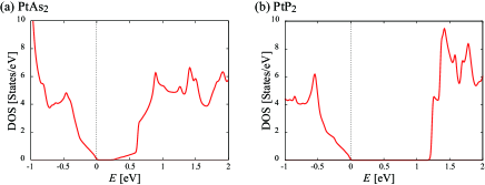
On the other hand, in the electron doped case, especially for PtP2, the Fermi surface is gathered around the point meaning that the portion of the bands around the zone center is flat in this case. As seen in Fig.1(d), the conduction band of PtP2 indeed has a very flat bottom that extends over a large portion of the three dimensional Brillouin zone, as schematically depicted in Fig.1(f). This is also clearly seen in the density of states (DOS) of PtP2 shown in Fig.3(b), which rises sharply at the conduction band edge, as if the material were a 2D system. Thus, the conduction bands of PtP2 have an ideal three dimensional pudding-mold shape.
As discussed in ref.Kuroki , pudding-mold type band is ideal for obtaining good thermoelectric properties, especially the power factor. A large thermopower is generally obtained when the velocity of electron and hole excitations near the Fermi level have large difference. When the Fermi level sits close to the band edge, the ratio can in general be large, but the absolute values of the velocities are usually small and also the Fermi surface is small, so that the conductivity is small. For the pudding-mold type band, on the other hand, the large density of states at the top of the band prevents the Fermi level from going down rapidly even when a large amount of carriers (holes in the present case) is doped. This is good for thermopower in that the Fermi level stays near the bending point of the band even when the Fermi surface volume is large. When the Fermi level sits close to the bending point of the pudding mold type band, ratio is large, resulting in a large Seebeck coefficient. At the same time, the conductivity becomes large due to the large Fermi surface volume and the dispersive portion (mainly below the Fermi level) of the bands. In this manner, the coexistence of large Seebeck coefficient and large conductivity is realized for a wide range of hole doping rate.
We now proceed to the calculation of the Seebeck coefficient for PtAs2 and PtP2. The Seebeck coefficient is calculated within the Boltzmann’s equation approach using the obtained tightbinding band structure. In this approach, tensors of the Seebeck coefficient and the conductivity are given as,
| (1) |
| (2) |
where is the elementary charge, is the temperature、tensors , are given as
| (3) |
Here, is the band dispersion, is the group velocity, is the quasiparticle lifetime, is the Fermi distribution function, and is the Fermi level (chemical potential). In the present study, we approximate as a constant, so that it cancels out in the Seebeck coefficient. We simply write and as and , respectively. and thus the power factor contain the constant , whose absolute value is not determined. Therefore, we only discuss the values of the power factor normalized by its maximum value as a function of the doping rate.
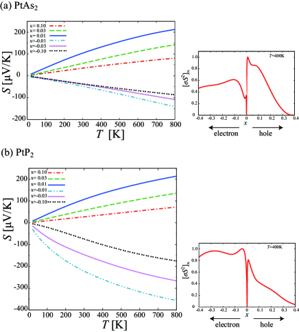
In Fig.4, we show the Seebeck coefficient against temperature for the two materials. It can be seen that the Seebeck coefficient monotonically increases with temperature, in contrast to a similar calculation for PtSb2Mori , and reaches V/K for both PtAs2 and PtP2, for the hole doping rate of and at temperature 800K. This is indeed due to the combination of the ideal band shape, together with the large band gap.
We also consider the case of electron doping, since the conduction band seems to have an ideal pudding mold type band structure for PtP2. The Seebeck coefficient for PtP2 indeed exceeds V/K already at 300K, and reaches a very large value of V/K at 800K for ( implies electron doping). The superiority of the electron doped PtP2 can further be seen in the doping dependence of the normalized power factor at 400K also shown in Fig.4. While the hole doped regime gives a better power factor for PtAs2, in PtP2 the electron doped regime gives larger and more persisting power factor compared to that in the hole doped regime. Based on these results, we expect good thermoelectric properties in PtP2 once sufficient amount of electrons is doped.
To summarize, we have studied the band structure and the Seebeck coefficient of MPn2 in an attempt to search for materials with thermoelectric properties better than PtSb2. We find that PtAs2 and PtP2 are good candidates with larger band gap, while Pd and Ni based compounds are not expected to exhibit good performance. Quite recently, the thermoelectric properties of the hole doped Pt1-xRhxAs2 has been measured experimentally, in which a large and monotonically increasing Seebeck coefficient at high temperature is foundKudoPtAs2 . The combination of this with the metallic behavior of the resistivity results in a very large power factor of 65W/cmK2 at K.
We are grateful to M. Nohara and K. Kudo for valuable discussion. H.S. acknowledges support from JSPS.
References
- (1) For a general review on the theoretical aspects as well as experimental observations of thermopower, see, G.D. Mahan Good Thermoelectrics, Solid State Physics 51, 81 (1997).
- (2) I. Terasaki, Y. Sasago and K. Uchinokura, Phys. Rev. B 56 R12685 (1997).
- (3) K. Kuroki and R. Arita, J. Phys. Soc. Jpn. 76 083707 (2007).
- (4) Y. Nishikubo, S. Nakano, K. Kudo, and M. Nohara, Appl. Phys. Lett. 100, 252104 (2012).
- (5) P.R. Emtage, Phys. Rev. B 138, A246 (1965).
- (6) K. Mori, H. Usui, H. Sakakibara, and K. Kuroki, AIP Advances 2, 042108 (2012).
- (7) K. Mori, H. Sakakibara, H. Usui, and K. Kuroki, arXiv:1304.2526, to be published.
- (8) H. Usui, K. Kuroki, S. Nakano, K. Kudo, and M. Nohara, arXiv:1211.7176, to be published.
- (9) P. Blaha, K. Schwarz, G.K.H. Madsen, D. Kvasnicka, and J. Luitz, Wien2k: An Augmented Plane Wave + Local Orbitals Program for Calculating Crystal Properties (Vienna University of Technology, Wien, 2001). Here we take , 1024 -points, and adopt the exchange correlation functional introduced by J. P. Perdew , K. Burke, and M. Ernzerhof [Phys. Rev. Lett. 77, 3865 (1996)].
- (10) The strucural data are taken from the following references : PtSb2, PtBi2, PdAs2, PdSb2 ; Nathaniel E. Brese, H.G. Von Schnering,. Z. Anorg. Allg. Chem., 620, 393 (1994), NiP2, NiAs2; Paul C. Donohue, Tom A. Bither, Howard Sargent Young,. Inorganic. Chemistry., 7, 998-1001(1968), PtAs2 ; Szymanski J.T,. Can. Mineral., 17, 117-123 (1979). PtP2 ; Schmidt T, Lutz H.D, Honle W,. Z. Kristallogr., 190, 143-146, (1990)
- (11) N. Marzari and D. Vanderbilt, Phys. Rev. B 56, 12847 (1997); I. Souza, N. Marzari, and D. Vanderbilt, Phys. Rev. B 65, 035109 (2001). The Wannier functions are generated by the code developed by A. A. Mostofi, J. R. Yates, N. Marzari, I. Souza, and D. Vanderbilt, (http://www.wannier.org/).
- (12) J. Kunes, R. Arita, P. Wissgott, A. Toschi, H. Ikeda, and K. Held, Comp. Phys. Commun. 181 1888 (2010).
- (13) K. Kudo, S. Nakano, T. Mizukami, K. Kajisa, K. Niitani, T. Takabatake, and M. Nohara, preprint.