Calculating the electromagnetic characteristics of bifacial optical nanomaterials
Abstract
We introduce a formalism that describes the interaction of light with bifacial optical nanomaterials. They are artificial noncentrosymmetric materials in which counter-propagating waves behave differently. We derive electromagnetic material parameters for uniaxial crystalline media in terms of the complex transmission and reflection coefficients of a single layer of the constituent nanoscatterers, which makes the numerical evaluation of these parameters very efficient. In addition, we present generalized Fresnel coefficients for such bifacial nanomaterials and investigate the fundamental role of higher-order electromagnetic multipoles on the bifaciality. We find that two counter-propagating waves in the material must experience the same refractive index, but they can have dramatically different wave impedances. The use of our model in practice is demonstrated with a particular example of a bifacial nanomaterial that exhibits a directional impedance matching to the surrounding medium.
I Introduction
Optical nanomaterials are artificial substances with subwavelength-sized unit cells that contain specially designed nanoparticles (artificial atoms). Light propagation in such a material is fully determined by the way electromagnetic waves are scattered and absorbed by the nanoparticles. The optical characteristics of the material can be described using effective material parameters, such as refractive index and wave impedance when the nanomaterial can be treated as homogeneous. For a given nanomaterial design, these parameters are commonly retrieved by calculating the light transmission and reflection by a slab of such nanomaterial.Menzel et al. (2008a); Smith et al. (2002); Menzel et al. (2008b) Using these retrieval procedures, certain nanomaterials have been designed to exhibit extreme values for the material parameters, which cannot be found in nature.Pshenay-Severin et al. (2009); Choi et al. (2011); Silveirinha and Engheta (2007); Yuan et al. (2007); Rockstuhl et al. (2009); Paul et al. (2009); Li et al. (2013) The commonly used retrieval procedures rely upon the assumption that the nanomaterial is free of spatial dispersion and, thus, treatable in terms of standard Fresnel transmission and reflection coefficients. These assumptions, however, may not hold for materials composed of asymmetric nanoscatterers, such as typical split-ring-resonators used to obtain artificial magnetism.Gompf et al. (2012)
Nanomaterials in which two counter-propagating optical waves see the medium differently belong to a specific class of optically bifacial nanomaterials. The nanoscatterers in these materials are not centrosymmetric. In this work, we consider uniaxial noncentrosymmetric nanomaterials. More complicated nanomaterials, such as those composed of chiral nanoparticles, are left out of the scope of the present paper. Although asymmetric scatterers have been widely studied in terms of their scattering propertiesGrahn et al. (2013a); Pakizeh and Käll (2009), magnetic near-field enhancementPakizeh et al. (2008); Pakizeh (2012), localized absorptionAntosiewicz et al. (2012), color switchingShegai et al. (2011); Lavasani and Pakizeh (2012) and mimicking electromagnetically induced transparencyLiu et al. (2009); Bozhevolnyi et al. (2011); Liu et al. (2011), no adequate theory currently exists for the description of nanomaterials constructed of such scatterers. For example, for a bifacial nanomaterial, the standard Fresnel coefficients cannot be applied. In this paper, we develop the necessary formalism - that allows calculation of the material parameters and - and use it to investigate the key properties of such artificial bifacial media. In particular, we find that two counter-propagating waves in the material must experience the same refractive index, but they can have dramatically different wave impedances.
We apply our model to a particular example of optical nanomaterials consisting of metal nanodimers and verify the correctness of our model by rigorous numerical calculations. We also verify that in the limiting case of symmetric nanoscatterers, our model is in agreement with the results of the existing retrieval procedures.
II Theory
II.1 Effective material parameters
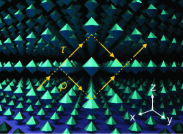
We start by considering a three-dimensional nanomaterial that consists of periodically arranged nanoscatterers in a transparent dielectric host medium of refractive index . This three-dimensional array can be thought as a set of two-dimensional nanoscatterer arrays, which are stacked in a certain common direction, as illustrated in Fig. 1. We choose the axis to point in this direction and the length of the unit cell along to be . For an optical plane wave propagating in the material, each two-dimensional nanoscatterer array can be treated as an infinitesimally thin sheet with a plane-wave transmission coefficient and reflection coefficient , which in general both depend on the wave propagation direction and polarization. As has been shown in Ref. Grahn et al., 2013b, these coefficients can be obtained by calculating the plane-wave transmission and reflection by an isolated two-dimensional nanoscatterer array in the host medium. As long as the periodicities within the array are sufficiently small compared to the local wavelength , there will be no coupling of diffraction orders between successive “crystal” planes in the material. Moreover, in the presence of sufficiently large spacing between neighboring nanoscatterers, the evanescent-wave coupling between the crystal planes can be safely neglected.Grahn et al. (2013b); Alaee et al. (2013); Chen (2012) Thus, in the analysis, there will locally be only two counter-propagating plane waves in the crystal, due to the finite reflection provided by each crystal plane. The optical response of the nanomaterial to a plane wave propagating in the host medium at an angle with respect to the axis is then fully determined by , , and . This is depicted in Fig. 2(a), where light waves are locally reflected back and forth between two nanoscatterer planes within the material. For another wave propagating at an angle of , as depicted in Fig. 2(b), reciprocity requires that and . For a general array of lossy nanoscatterers, the asymmetries and can hold. However, for uniaxial nanomaterials considered in this work, the symmetry requires that . For bifacial materials, the inequality can be the case, which allows the waves propagating in the and directions to behave differently.
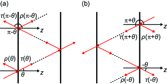
Each unit-cell thick layer in a nanomaterial is in our analysis characterized by the following propagation-direction dependent coefficients
| (1) |
| (2) |
where is the z component of the wave vector in the surrounding medium; is the wave number in vacuum. We remind that and depend on the polarization. The first coefficient, , describes the transmission through a single layer of thickness , whereas describes the reflection from this layer. Between two neighboring layers and , we denote the transverse component of the electric field for the forward and backward propagating waves by and , respectively. These fields are recursively related to each other asGrahn et al. (2013b)
| (3) | |||||
| (4) |
Using these equations, one can derive
| (5) |
where
| (6) |
Next we derive the effective material parameters that characterize the three-dimensional nanoscatterer array as a homogeneous, but spatially dispersive nanomaterial. The first such parameter is the refractive index . In the homogenized material, the transverse electric field of a propagating plane wave must satisfy
| (7) |
where is the z component of the effective wave vector. Combining Eqs. (5) and (7), we obtain
| (8) |
with . For nanomaterials which are not bifacial, Eq. (8) can be shown to be in perfect agreement with Eq. (6) of Ref. Menzel et al., 2008a.
The refractive index is obtained as
| (9) |
where the continuity of the tangential component of the wave vector is taken into account. This is one of the key results of this work. The choice of order and signs in Eqs. (8) and (9), to obtain physical solutions, are performed as described in Ref. Menzel et al., 2008a, i.e., using the continuity of the spectrum and requiring and to have positive imaginary parts. We notice that, since is symmetric with respect to the interchange between and , the effective refractive index is the same for any two counter-propagating waves. This finding can be understood as a consequence of reciprocity for the waves propagating inside the material. As we show next, the same symmetry does not hold for the effective wave impedance.
We derive the wave impedance of the nanomaterial by averaging the electromagnetic fields over a single period of the material in the direction. Irrespective of the field polarization, we use Eqs. (3) and (7) to express the component of the electric field that is transverse to the axis between two neighboring crystal planes as
| (10) | |||||
Since , and form a right-handed triad in the host medium, the transverse component of the magnetic field is
| (11) | |||||
where denotes the wave impedance of the host medium and
| (12) |
Notice that we define the reflection coefficient for the TM-polarization such that it has zero phase when the transverse components of the reflected and incident electric fields are in phase. By integrating Eqs. (10) and (11) with respect to over the interval from to we can calculate the averaged transverse electric and magnetic fields in the unit cell. Using the fact that , where denotes the mentioned averaging, we find the ratio between the averaged fields to be
| (13) |
In the homogenized material, the wave (on average) propagates at an angle . This angle, as determined by the Snell law , is obtained from
| (14) |
For the TE polarization, the total magnetic field is found from the transverse magnetic field by dividing it with . The total electric field is transverse for this polarization. Using Eq. (13), the effective wave impedance for the TE polarization becomes
| (15) |
Likewise, for the TM polarization the transverse electric field appearing in the numerator of Eq. (13) must be divided with and, thereby, we obtain
| (16) |
Notice that the quantities , and in Eqs. (15) and (16) have different values for TE and TM polarizations. Obviously, the impedances obtained for two counter-propagating waves are different in bifacial nanomaterials [since , when ].
Equations (9), (15) and (16) fully characterize the material. We have verified that for nanomaterials which are not optically bifacial, these equations yield exactly the same results as the retrieval procedure of Ref. Menzel et al., 2008a. The derivation in Ref. Menzel et al., 2008a, however, considers a plane-wave transmission through a nanomaterial slab, whereas the derivation presented here considers the plane waves propagating inside a bulk nanomaterial of an arbitrary shape.
In summary, the material parameters for a given bifacial nanomaterial design can be calculated as follows: The first step is to numerically or otherwise obtain the spectra of and , defined in Eqs. (1) and (2), for a single two-dimensional layer of nanoscatterers in the host medium. Next, one calculates the spectra of using Eq. (6). Thereafter a continuous spectrum of is calculated from Eq. (8). The spectrum of the refractive index follows from Eq. (9). With the refractive index at hand, the effective propagation angle in the material is solved from Eq. (14). Finally, depending on the chosen polarization, one uses either Eq. (15) or Eq. (16) to obtain the spectrum of the wave impedance.
II.2 Transmission and reflection at an interface between two bifacial nanomaterials
The transmission and reflection of an optical plane wave at a material boundary is usually described by using the standard Fresnel coefficients.Saleh and Teich (2007) However, it has been shown that even for strictly homogeneous noncentrosymmetric crystals that are free of spatial dispersion, a generalized form of these coefficients is required.Graham and Raab (1996) In the case of optically bifacial nanomaterials, the Fresnel coefficients must be modified as well, to take into account both the asymmetry of the unit cells and the resulting spatial dispersion.
Consider a boundary at between two bifacial materials with material parameters and , where the index refers to the material in question. A wave with a wave vector is incident from material 1 onto material 2, in which the wave propagates with the wave vector as depicted in Fig. 3. The magnitude of the wave vector is . For simplicity, we define and to denote the impedances for the waves propagating to the right and left, respectively, in Fig. 3. The vector complex amplitudes of the electric and magnetic fields for the incident () and transmitted () waves can be written as
| (17) | |||||
| (18) |
The wave vector of the reflected wave is . The reflected wave is therefore of the form
| (19) | |||||
| (20) |
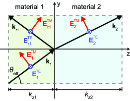
Applying the electromagnetic boundary conditions that require and at , we derive the generalized Fresnel transmission and reflection coefficients for the TE and TM polarizations as
| (21) | |||
| (22) | |||
| (23) | |||
| (24) |
where the subindex 12 indicates that the field is incident from material 1 onto material 2. As shown in the next section, the bifacial behavior is tightly connected to the excitation of higher-order multipoles. It has previously been suggested that special electromagnetic boundary conditions are required to deal with materials in which higher order multipoles can be excited.Graham and Raab (2000) Here, however, the ordinary boundary conditions are applied, since we allow the material parameters to depend on the propagation direction of the plane wave for which they are calculated. This provides a remarkable simplicity for the resulting Fresnel coefficients.
Using Eqs. (21)-(24) one can, for instance, calculate the transmission and reflection coefficients of an optically bifacial nanomaterial slab by taking into account multiple reflections. For a wave being incident from a semi-infinite material 1 onto a bifacial slab made of a material 2 of thickness and transmitted into a semi-infinite material 3, these coefficients are
| (25) | |||||
| (26) |
For any bifacial nanomaterial slab, the reflection coefficient for a wave incident from material 1 differs from that obtained for a wave incident from material 3 even when the materials 1 and 3 are the same, which can be seen by interchanging and in Eqs. (21)-(26). The transmission coefficient, however, is invariant with respect to this interchange, which ensures that the nanomaterial is reciprocal. Equations (21)-(26) enable one to verify the effective material parameters calculated by using Eqs. (9), (15) and (16). At the end of Sec. III, this verification is performed for a particular bifacial nanomaterial.
II.3 Electromagnetic multipoles
In this subsection, we show that for a nanomaterial to be optically bifacial, it is necessary that higher-order electromagnetic multipoles are excited in the nanoscatterers. The transmission and reflection coefficients of a two-dimensional array of nanoscatterers are related to the multipole excitations in each nanoscatterer. Here, for simplicity, we derive these coefficients for normal-incidence illumination of a nanoscatterer array in which both electric dipole and current quadrupoleGrahn et al. (2012a) moments are excited. Considering an -polarized incident wave, we write the complex amplitude for the component of the excited electric current density as
| (27) |
where and are integers that refer to a certain equivalent point-scatterer in a square lattice of period in the plane. In Eq. (27), is the component of the excited dipole moment and is the element of the current quadrupole dyadic.Grahn et al. (2012a) The contribution from the element of the quadrupole dyadic is neglected, as it does not radiate in the direction. For , no diffraction orders can appear, and Eq. (27) can be averaged in the plane to obtain
| (28) |
When replacing with , the evanescent near-field of the array is lost, whereas the far-field that determines the transmission and reflection of the array remains. In the Lorenz gauge, the component of the vector potential satisfies the wave equation
| (29) |
where and are the wave number and magnetic permeability, respectively, of the surrounding medium. Using the one-dimensional Green’s function,Dudley (1994) one can solve Eq. (29) for the vector potential and obtain
| (30) |
The electric far-field scattered by the array, , is related to the vector potential throughGrahn et al. (2012a)
| (31) |
The reflection coefficient for the array is obtained from Eqs. (30) and (31) by dividing the complex amplitude with the electric field amplitude of the incident wave at . The result is
| (32) |
The coefficients and are the electric dipole and current quadrupole polarizability components of the scatterers (see also Ref. Grahn et al., 2013a). For the transmission coefficient , the forward scattered field is superposed to the incident field at . Dividing this superposition field with the incident field, we obtain
| (33) |
Equations (32) and (33) give the normal-incidence transmission and reflection coefficients for an arbitrary two-dimensional array of nanoscatterers, provided that the array period is subwavelength-sized. Octupoles and other higher-order multipoles, which may be excited in particular nanoscatterer designs,Curto et al. (2013); Kaelberer et al. (2010) can be included by simply adding more terms in the expansion of . These multipoles, however, are often negligible for subwavelength-sized nanoparticles.
Important conclusions can now be made from Eqs. (32) and (33) regarding the effect of multipoles on optically bifacial and non-reflective nanoparticle arrays. The first conclusion is that complete suppression of reflection requires at least the excitation of current quadrupoles in the nanoparticles. We recall that the current quadrupoles include both traditional electric quadrupoles and magnetic dipoles, which are electromagnetic multipoles of the same order.Grahn et al. (2012a) By designing the scatterers such that , the reflection can be brought to zero. This is precisely what happens in so-called metamaterial perfect absorbers.Zeng et al. (2013) In general, both the transmission and absorption are non-zero. Another conclusion is that the excitation of quadrupoles or other higher-order multipoles are necessary for bifacial behavior (for the reflection coefficient to depend on the side of illumination). This is seen by noting that, due to reciprocity, in Eq. (33) must be the same for both illumination sides. Therefore, if , also must be the same for both illumination sides, and so must be the reflection coefficient , too.
III Numerical studies
In this section, we use the introduced theory to analyze a particular example of an optically bifacial nanomaterial constructed of gold nanodimers.Grahn et al. (2012b, 2013a) These nanodimers consist of two axis-aligned discs as depicted in Fig. 4(a). The thickness of both discs is chosen to be nm and the surface-to-surface separation between the discs is nm. The diameters of the discs are chosen as nm and nm, such that the resonances of the discs occur at different frequencies. In the material, the nanodimers are arranged in a cubic lattice with a period of nm and placed in a surrounding dielectric of refractive index , corresponding to that of glass. The nanodimer dimensions and the lattice geometry are chosen such that the material is impedance-matched to the surrounding medium when illuminated from the side of the smaller disc.
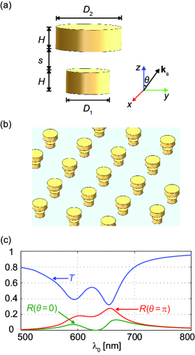
We start by calculating the complex transmission and reflection coefficients of a single two-dimensional array of the nanodimers in glass [see Fig. 4(b)] using the computer software COMSOL Multiphysics. The spectrum of the relative electric permittivity of gold is taken from Ref. Johnson and Christy, 1972. The intensity transmission and reflection spectra of this array at normal incidence are depicted in Fig. 4(c). At a vacuum wavelength of nm the reflection from the smaller-disc side () is strongly suppressed, whereas the reflection from the other side () is considerable.
Using the theory presented in section II.3, we can fully explain this bifacial behavior of the nanodimer array in terms of the electromagnetic multipole excitations. The multipole excitations in the array are extracted from the electric field distribution inside the scatterers as described in Ref. Grahn et al., 2012a. The electric dipole and current quadrupole moments are obtained from the multipole coefficients as
| (34) | |||||
| (35) | |||||
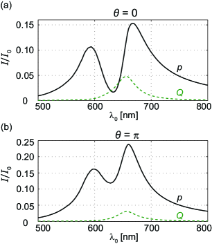
where and are the electric and magnetic multipole coefficients, respectively, described in detail in Ref. Grahn et al., 2012a. In Fig. 5, we show the normalized intensity of the field radiated in the backward direction separately by the dipoles and current quadrupoles, as obtained by calculating the squared moduli of the individual terms in Eq. (32). The actual reflection shown in Fig. 4(c) is the result of interference between the two multipole waves as given by Eq. (32). The magnitudes of multipoles of higher orders than the current quadrupole are negligibly small. From Fig. 5(a), we see that in the region of nm, the dipole and quadrupole waves have equal amplitudes. These two waves oscillate out of phase and interfere destructively, providing the suppressed reflection in Fig. 4(c). In contrast, for the opposite propagation direction, , the dipole contribution is much larger than the quadrupole one over the whole spectral range considered [see Fig. 5(b)]. Consequently, the reflection is significant everywhere in this wavelength range.
In order to calculate the effective electromagnetic material parameters for the considered three-dimensional nanomaterial, we use Eqs. (9), (15) and (16) with the complex transmission and reflection coefficients that are numerically obtained for the two-dimensional array of the dimers. The effective refractive index and impedance are expected to depend on both the angle and the polarization direction of the light. Consequently, we consider both TE- and TM-polarized waves and a large enough set of propagation angles in the host medium, choosing the values of 0, , , , , and . As explained in Sec. II.1, it is sufficient to evaluate the refractive index only for , because of the symmetry . Before discussing our results, we emphasize that we have verified the obtained material parameters by doing rigorous numerical calculations for a five-layer thick nanomaterial slab and by comparing those calculations with the results obtained by applying Eqs. (21)-(26) with the evaluated material parameters. The agreement is perfect, as will be shown later on in this section.
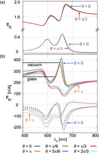
For the TE polarization, with the electric field perpendicular to the dimer axis, the calculated spectra of the refractive index and the wave impedance are shown in Figs. 6(a) and 6(b), respectively. The real parts of these complex quantities are shown by solid lines, while the imaginary parts are shown by dashed lines. It can be seen that, for this polarization, the refractive index is nearly independent of the light propagation direction. This feature can be understood by noting that the modal excitations in the individual discs can only slightly depend on the angle of incidence of the light. In the refractive index spectra, one can clearly distinguish the dipole resonances of the two discs composing the dimers.
In contrast to the refractive index, the wave impedance, as expected, depends on the propagation direction quite significantly [see Fig. 6(b)]. At a wavelength of about 630 nm, the wave impedance for is essentially real-valued and quite well matched to that of the surrounding glass, which means that the light reflection at a glass-nanomaterial interface will be suppressed [see Eq. (23)]. The smaller discs are in this case pointed towards the interface. On the other hand, if the larger discs are those which are closer to the interface, the interface reflects light significantly, as follows from a completely different value of wave impedance for at this wavelength. Still one can see that in the range of (or ) the material can be considered to be nearly spatially non-dispersive. It is nonetheless quite obvious that the material is optically bifacial.
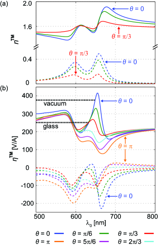
The calculated spectra for the refractive index and the wave impedance corresponding to TM polarized light are shown in Fig. 7. For this polarization, the refractive index changes significantly with the propagation angle , as shown in Fig. 7(a). This is a consequence of the fact that the component of the electric field interacts non-resonantly with the nanodimers. Hence, for angles approaching , the resonant interaction of the wave with the dimers gradually disappears. For the propagation directions and , the wave impedances are as expected identical to those for the TE polarization. However, for the TM polarization, the wave impedance changes more with increasing than for the TE polarization. At nm, we still have quite good impedance-matching of the material to glass at .
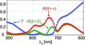
We have verified the validity of the obtained material parameters and the expressions for them in Eqs. (9), (15) and (16) by using Eqs. (21)-(26) to calculate the transmission and reflection of light by a nanomaterial slab in vacuum. The slab has a thickness of 750 nm and contains five nanodimer layers [each layer is as the one in Fig. 4(b)] embedded in glass. The calculated intensity transmission and reflection spectra of this slab are depicted by solid lines in Fig. 8. For comparison, we use COMSOL to directly calculate the transmission and reflection by the slab. The results of these calculations are presented in Fig. 8 by stars. These results are seen to be in perfect agreement with the results obtained using our effective material parameters. The suppressed reflection at nm originates from the fact that at this wavelength the nanomaterial is approximately impedance-matched to vacuum (see Figs. 6 and 7).
IV Conclusions
We have introduced a theoretical model for calculating the electromagnetic characteristics of designed bifacial optical nanomaterials that are composed of noncentrosymmetric nanoparticles with a single symmetry axis. In general, these characteristics depend on the propagation direction of light, and for bifacial nanomaterials they are different for two counter-propagating waves. Our approach enables direct evaluation of the material’s refractive index and wave impedance from the transmission and reflection coefficients of a single crystal plane of the constituent nanoscatterers. This makes the required numerical calculations fast. Taking into account the dependence of the material parameters on the light propagation direction, we have derived generalized Fresnel coefficients that describe the light transmission and reflection at the surface of a bifacial nanomaterial. We have found that in order to create an optically bifacial nanomaterial, it is necessary to use nanoscatterers in which light can efficiently excite higher-order electromagnetic multipoles. One remarkable finding is that inside such a nanomaterial, two counter-propagating waves necessarily see equal refractive indices, while they can experience quite different wave impedances.
The practical application of the theory was demonstrated with a particular example of a bifacial nanomaterial composed of metal-disc nanodimers. Using the model, we have designed and characterized a material that is impedance-matched to the surrounding medium (glass and vacuum) for a wave propagating in a certain direction, but not for a counter-propagating wave.
This work opens up the possibility to comprehensively describe and design uniaxial bifacial optical nanomaterials. The asymmetry of the unit cells in such materials can provide the substance with an extraordinary electromagnetic response that is not possible to find in natural materials. For example, a nanomaterial slab can be designed to have a desired spectrum of the refractive index and/or to reflect light only by one of its surfaces. The latter feature can be of interest for imaging and energy-harvesting applications, including ultrathin wide-angle bifacial antireflection coatings and high-efficiency solar cells.
Acknowledgements.
This work was funded by the Academy of Finland (Project No. 134029).References
- Menzel et al. (2008a) C. Menzel, C. Rockstuhl, T. Paul, F. Lederer, and T. Pertsch, Phys. Rev. B 77, 195328 (2008a).
- Smith et al. (2002) D. R. Smith, S. Schultz, P. Markoš, and C. M. Soukoulis, Phys. Rev. B 65, 195104 (2002).
- Menzel et al. (2008b) C. Menzel, C. Rockstuhl, T. Paul, and F. Lederer, Applied Physics Letters 93, 233106 (2008b).
- Pshenay-Severin et al. (2009) E. Pshenay-Severin, U. Hübner, C. Menzel, C. Helgert, A. Chipouline, C. Rockstuhl, A. Tünnermann, F. Lederer, and T. Pertsch, Opt. Lett. 34, 1678 (2009).
- Choi et al. (2011) M. Choi, S. H. Lee, Y. Kim, S. B. Kang, J. Shin, M. H. Kwak, K.-Y. Kang, Y.-H. Lee, N. Park, and B. Min, Nature 470, 369 (2011).
- Silveirinha and Engheta (2007) M. Silveirinha and N. Engheta, Phys. Rev. B 75, 075119 (2007).
- Yuan et al. (2007) H.-K. Yuan, U. K. Chettiar, W. Cai, A. V. Kildishev, A. Boltasseva, V. P. Drachev, and V. M. Shalaev, Opt. Express 15, 1076 (2007).
- Rockstuhl et al. (2009) C. Rockstuhl, C. Menzel, T. Paul, and F. Lederer, Phys. Rev. B 79, 035321 (2009).
- Paul et al. (2009) T. Paul, C. Rockstuhl, C. Menzel, and F. Lederer, Phys. Rev. B 79, 115430 (2009).
- Li et al. (2013) Z. Li, M. Mutlu, and E. Ozbay, Journal of Optics 15, 023001 (2013).
- Gompf et al. (2012) B. Gompf, B. Krausz, B. Frank, and M. Dressel, Phys. Rev. B 86, 075462 (2012).
- Grahn et al. (2013a) P. Grahn, A. Shevchenko, and M. Kaivola, J. Europ. Opt. Soc. Rap. Public. 8, 13009 (2013a).
- Pakizeh and Käll (2009) T. Pakizeh and M. Käll, Nano Letters 9, 2343 (2009).
- Pakizeh et al. (2008) T. Pakizeh, A. Dmitriev, M. S. Abrishamian, N. Granpayeh, and M. Käll, J. Opt. Soc. Am. B 25, 659 (2008).
- Pakizeh (2012) T. Pakizeh, J. Opt. Soc. Am. B 29, 2446 (2012).
- Antosiewicz et al. (2012) T. J. Antosiewicz, S. P. Apell, C. Wadell, and C. Langhammer, The Journal of Physical Chemistry C 116, 20522 (2012).
- Shegai et al. (2011) T. Shegai, S. Chen, V. D. Miljković, G. Zengin, P. Johansson, and M. Käll, Nature Commun. 2, 481 (2011).
- Lavasani and Pakizeh (2012) S. H. A. Lavasani and T. Pakizeh, J. Opt. Soc. Am. B 29, 1361 (2012).
- Liu et al. (2009) N. Liu, L. Langguth, T. Weiss, J. Kästel, M. Fleischhauer, T. Pfau, and H. Giessen, Nature Mater. 8, 758 (2009).
- Bozhevolnyi et al. (2011) S. I. Bozhevolnyi, A. B. Evlyukhin, A. Pors, M. G. Nielsen, M. Willatzen, and O. Albrektsen, New Journal of Physics 13, 023034 (2011).
- Liu et al. (2011) N. Liu, M. Hentschel, T. Weiss, A. P. Alivisatos, and H. Giessen, Science 332, 1407 (2011).
- Grahn et al. (2013b) P. Grahn, A. Shevchenko, and M. Kaivola, arXiv:1303.6432 (2013b).
- Alaee et al. (2013) R. Alaee, C. Menzel, A. Banas, K. Banas, S. Xu, H. Chen, H. O. Moser, F. Lederer, and C. Rockstuhl, Phys. Rev. B 87, 075110 (2013).
- Chen (2012) H.-T. Chen, Opt. Express 20, 7165 (2012).
- Saleh and Teich (2007) B. E. A. Saleh and M. C. Teich, Fundamentals of photonics, 2nd ed. (Wiley, New Jersey, 2007).
- Graham and Raab (1996) E. B. Graham and R. E. Raab, J. Opt. Soc. Am. A 13, 1239 (1996).
- Graham and Raab (2000) E. B. Graham and R. E. Raab, Proc. R. Soc. Lond. A 456, 1193 (2000).
- Grahn et al. (2012a) P. Grahn, A. Shevchenko, and M. Kaivola, New Journal of Physics 14, 093033 (2012a).
- Dudley (1994) D. G. Dudley, Mathematical foundations for electromagnetic theory (IEEE Press, New York, 1994).
- Curto et al. (2013) A. G. Curto, T. H. Taminiau, G. Volpe, M. P. Kreuzer, R. Quidant, and N. F. van Hulst, Nat. Commun. 4, 1750 (2013).
- Kaelberer et al. (2010) T. Kaelberer, V. A. Fedotov, N. Papasimakis, D. P. Tsai, and N. I. Zheludev, Science 330, 1510 (2010).
- Zeng et al. (2013) Y. Zeng, H.-T. Chen, and D. A. R. Dalvit, Opt. Express 21, 3540 (2013).
- Grahn et al. (2012b) P. Grahn, A. Shevchenko, and M. Kaivola, Phys. Rev. B 86, 035419 (2012b).
- Johnson and Christy (1972) P. B. Johnson and R. W. Christy, Phys. Rev. B 6, 4370 (1972).