Strain engineering of topological properties in lead-salt semiconductors
Abstract
Rock-salt chalcogenide SnTe represents the simplest realization of a topological insulator where a crystal symmetry allows for the appearence of topologically protected metallic states with an even number of Dirac cones on high-symmetry crystal surfaces. Related rock-salt lead chalcogenides have been predicted as well to undergo a phase-transition to a topological crystalline insulating phase after band inversion induced by alloying and pressure. Here we theoretically predict that strain, as realized in thin films grown on (001) substrates, may induce such topological phase-transitions. Furthermore, relevant topological properties of the surface states, such as the location of the Dirac cones on the surface Brillouin zone or the decay length of edge states, appear to be tunable with strain, with potential implications for technological devices benefiting from those additional degrees of freedom.
pacs:
73.20.At, 71.20.Nr, 73.90.+f, 71.70.EjTopological band-insulators are new states of matter where the electronic structures display non-trivial topological features leading to the appearence of symmetry-protected metallic edge states which feature graphene-like Dirac cones. Hasan_RMP ; Qi_RMP ; Moore_nature ; Fu_PRL As a result of their non-trivial topological invariants (based on the wave-function “wrapping” of the Brillouin zone), these surface states are exceptionally robust against perturbations. Moreover, the spin-orbit coupling (SOC), which ultimately lies at the origin of the phenomenon, makes the surface states to show a single spin-state for each momentum, paving the way to spin-polarized currents of interest in spintronics.Hasan_RMP ; Qi_RMP ; Moore_nature ; Fu_PRL After the discovery of the so-called topological insulators, where the unusual metallic states are protected by time-reversal symmetry, it has been realized that other fundamental symmetries may allow for the existence of topologically-protected states of matterFu_TCI ; Slager . In particular, it has been shown that the narrow-gap IV-VI semiconductor SnTe is a topological crystalline insulator (TCI) in its face-centered-cubic () structure, where a mirror symmetry is responsible for the appearence of an even number of Dirac cones on (001), (011) and (111) surfacesHsieh_ncomm ; Tanaka_nature . With the only exception of (111) surfaces, these Dirac cones are situated, in contrast to topological insulators, off the time-reversal-invariant momenta along a high-symmetry line of the surface Brillouin zone contained in a mirror plane of the crystal structure. As reported recently, this unique feature of SnTe arises from the hybridization of two distinct Dirac cones projected on the (001) and (011) surfacesTanaka_nature ; Fu_111 ; Tanaka_prb .
Even though closely related lead-salt semiconductors PbS, PbSe and PbTe display the same symmetry properties as SnTe, their electronic structures appear to be topologically trivial at equilibrium volume. Metallic surface states in these compounds do not show up due to the absence of a bulk band inversion, that is generally believed to be caused by SOCHsieh_ncomm . So far, the possibility to induce topological transitions in these systems has been explored by alloying lead chalcogenides PbTe and PbSe with Sn, thus triggering the required band inversion while keeping the same crystal structureTanaka_prb ; Xu_ncomm ; Dziawa_nmat ; Wojek . Interestingly, the location of the Dirac cones on the (001) surfaces of Pb1-xSnxTe has been found to vary in space when changing the composition ratio , providing an additional degree of freedom with potential applications for spintronic devicesTanaka_prb . On the other hand, it has been recently suggested that the band inversion arises from the interplay of SOC and an “asymmetric” hybridization between cation and anion orbitalsnostro ; as such, a topological phase-transition could be naturally attained by applying external pressure or strain, which would directly affect the aforementioned hybridization, as long as the mirror symmetries are preserved. Specifically, all lead chalcogenides have been predicted to become TCIs upon applied pressures in the rangenostro . The effect of strain on the topological properties of this class of narrow-band semiconductors, however, has not been addressed in details yet, even though a strain-induced TCI transition has been recently predicted in PbTehuang_matexp , whereas strain engineering of topological order has been already considered in several materials including ternary Heusler, zinc-blende and cubic semiconducting compoundsFelser_zhang ; winterfield ; feng .
Films of lead-salt chalcogenides have been long fabricated using a variety of techniques, ranging from liquid phase epitaxy to molecular beam epitaxy, and several substrates have been usedsuperlattices ; MBE ; Mukherjee . Due to their rock-salt structures, lead-salt compounds have (001) natural cleavage planes and tend to grow in the (001) growth orientation, although the (111) growth orientation has also been reported. Alkali-halide substrates such as NaCl, NaBr, NaI, KCl, KBr, KI, LiF have been widely used for IV-VI-compound (001)-oriented epitaxial thin filmssuperlattices , since they mainly have the same rock-salt structure and comparable lattice constants; other substrates such as (111)Si or BaF2 have been used for the growth of (111)-oriented filmsMBE .
In this work we theoretically demonstrate, by means of ab initio-based tight-binding (TB) and accurate density-functional theory (DFT) calculations, that all lead-salt chalcogenides may be turned into topological insulators at reasonable values of strain when grown on (001)-oriented substrates. The -space location of the Dirac cones appear to be dependent on the strain, thus suggesting an alternative path for the tunability of topological properties in TCIs, as opposed to alloying or pressure, and envisaging novel spintronic applications based e.g. on piezoelectric substrates. The critical thickness at which topological edge states appear is found to be of the order of close to the strain-induced topological transition. However, as the bulk gap increases upon applying larger strain, the decay length of surface states is largely reduced, suggesting that topological thin films may be engineered by a proper choice of the substrate. On the other hand, in films epitaxially grown on (111) substrates an insulator to semi-metal transition, triggered by a rhombohedral distortion, is predicted to occur before any band inversion — and hence any topological transition — can appear.
Methods. The systematic analysis of strain effects in the rock-salt IV-VI class of compounds has been performed by resorting to an ab initio-based relativistic parametrization of a nearest-neighbor () TB model including , and statesLent . Structural deformations as induced by strain have been taken into account assuming an ideal thin strained overlayer grown over a substrate which determines the lattice constant parallel to the interface plane. Within these assumptions, interfacial strain and perpendicular strained lattice constant are given by and , where are the equilibrium lattice constants and the constants have been estimated from the experimental elastic constants and elastic1 ; elastic2 asVandeWalle :
| (1) | |||||
| (2) |
All TB parameters have been accordingly rescaled following Harrison’s rulesHarrison , , where are the ion-ion distances modified by the applied strain, label the orbital states and are the scaling exponents for ---, -- and - hopping interactions, respectively.
In order to benchmark the reliability of our TB calculations, we performed accurate DFT calculations with HSE hybrid functionalhybrid , as implemented in VASP vasp1 ; vasp2 , for selected values of the strain. Hybrid functionals improve signicantly with respect to the local (LDA) and semi-local (GGA) approximations, especially for narrow band-gap semiconductors and lead chalcogenidesCardona ; Kresse . Total-energy calculations were performed to optimize the out-of-plane lattice parameter, structure while progressively changing in-plane lattice constants in order to mimic strain conditions imposed by a well-defined substrate. The energy cutoff for the plane-wave expansion was 600 eV and an Monkhorst- Pack k-point grid was used. Calculations with the HSE hybrid functional are computationally very demanding and, thus, were used for bulk states only; however, realistic and accurate surface states have been calculated by means of a Wannier-functions parametrization of DFT band structure, as derived via a Maximally-localized Wannier function algorithmwannier90 .
Results. Lead chalcogenides Pb, with S, Se, Te, have a simple rock-salt structure with the fundamental band gap located at four equivalent points in the rhombohedral setting. At their equilibrium volumes, they are not TCIs, the ordering of conduction and valence bands not being inverted (as opposed to SnTe). However, they are well known for their peculiar electronic structures, the small band-gap arising from a strong level repulsion at the points of the Brillouin zone due to the presence of occupied Pb-6 band below the top of the valence bandWei ; Cardona ; Kresse . The band ordering close to the Fermi level is then determined by the interplay of hybridizations between cation () states with anion () states, that has been predicted to be strongly asymmetric in lead-salt chalcogenides and SnTe, whereas a sizeable SOC eventually causes the opening of the gapnostro ; huang_matexp . In the trivial insulating phase, which is smoothly connected to the atomic limit of infinitely far ions, the valence band maximum (VBM) is expected to have strong Pb- and anion- character, while the conductance band minimum (CBM) displays strong Pb- and anion- character. For the TCI SnTe, the ordering is reversed mainly because of a stronger hybridization (also due to its smaller equilibrium volume as opposed to PbTe), rather than by SOC alone (which is indeed smaller in Sn than in Pb).
The presence of mirror planes in the structure combined with band-inversion at points implies a non-zero mirror Chern number which, in turn, dictates the existence of spin-polarized surface states with opposite mirror eigenvalues appearing on (001), (011) and (111) surfaces which preserve the relevant mirror-symmetry operationsHsieh_ncomm ; Fu_111 ; Safaei . When considering strain in (001) and (111) oriented films, it is more convenient to discuss their crystal and electronic structures in a tetragonal and hexagonal setting respectively, with the fundamental gap located at four equivalent points or and three equivalent points, respectively. All these high-symmetry points are still related by the relevant mirror simmetries giving rise to nontrivial mirror Chern numbers. As a consequence, if a band inversion is induced by biaxial strain in the (001) plane, a TCI is realized. On the other hand, biaxial strain in the (111) plane may well cause a rhombohedral distortion, and in principle a band inversion may appear in an even/odd number high-symmetry point ( and/or ), thus meaning the onset of a TCI/ topological order.
(001)-oriented systems. The strain deformation mainly affects the anion-cation distances, and consequently their hopping interactions; specifically, a compressive in-plane strain reduces the distances in the plane while increasing the distances along the perpendicular axis (a tensile strain doing the opposite). Furthermore, a significant volume effect is predicted as , implying a positive/negative pressure effect for compressive/tensile strain. We verified the accuracy of the predicted structural deformations by comparing with ab initio calculations, which systematically predict larger volumes in PbTe and PbSe (1.4% and 0.5% at , respectively), while a slightly smaller volume is found in PbS (-0.4% at ).
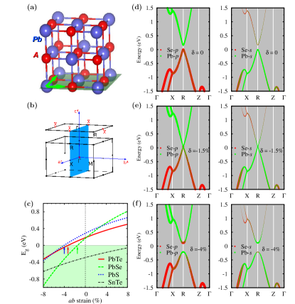
The combination of these structural deformations, directly acting upon the asymmetric hybridizationnostro , causes a closure of the gap followed by a reopening with an inversion of conductance and valence bands upon compression. Conversely, upon tensile strain the band gap increases for Pb non-inverted band structures mainly because of the “negative pressure” effect (see Fig. 1). The estimated critical strains from TB parametrizations are for Te, Se, S respectively. Our DFT calculations predict slightly larger critical strains for PbTe () and PbSe (), while at the band inversion in PbS has already occurred. The projected and characters of the bands, as shown in Fig. 1 for PbSe, further support the role of the asymmetric hybridization mechanism in causing the band-inversion phenomenon. (001)-strained lead-salt chalcogenides stay insulating at least up to a compressive strain of the order of .
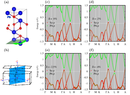
(111)-oriented systems. In addition to the volume and anion-cation distances modulation, a rhombohedral distortion of the unit cell, characterized by the angle , is induced by a biaxial strain along the (111) plane. The rhombohedral angle evolves as , and gets smaller/larger than 60∘ at compressive/tensile strain. The main consequence of this rhombohedral distortion is to make the and points ( and in rhombohedral setting) inequivalent, thus allowing, in principle, for topological transitions of or TCI order if a band inversion occurs at or rather than at and points, respectively. When looking at the strained electronic structures of (111)-oriented compounds, the energy differences between VBM abd CBM at and decrease (increase) under compressive (tensile) strain for all lead-salt chalcogenides. However, hole and electron pockets appear before any band inversion takes place, as shown in Fig. 2. Therefore, the topological phase-transitions never occur, being hindered by a transition to a semi-metal phase .
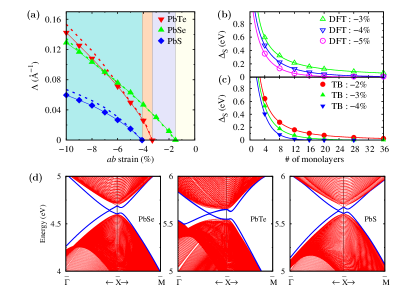
Surface states. Due to the presence of (110) mirror planes, the band inversion at points in the strained (001)-compounds implies a non-zero mirror Chern number and the existence of two pairs of spin-polarized surface states with opposite mirror eigenvalues along the lines , crossing at four Dirac points off the high-symmetry points .Hsieh_ncomm ; Fu_111 ; Safaei This is a consequence of the unique electronic topology of topological crystal insulators protected by mirror symmetries, and its realization in rock-salt chalcogenides is due to the projection of two () points onto the same momentum on the surface Brillouin zone; the resulting interaction between -valleys is the main responsible for the displacement of the Dirac cones away from the high-symmetry points , while a surface-state hybridization (which is symmetry-prohibited along the mirror plane) forbids any band-crossing but along the line. The location of Dirac points away from has been recently deduced in SnTe by introducing a model including inter-valley scattering up to linear terms in Fu_111 . Within this approach, along the high-symmetry line , where describe the energies of two Dirac cones centred at and their hybridization, respectively, while is the Dirac velocity at . The quantity also describes the energy separation between surface conductance and valence bands at , and as such it strongly correlates to the bulk gap.Tanaka_prb ; Fu_111 Therefore, the strain control of the bulk gap, as shown in Fig. 1, should in principle also allow for a tunability of the Dirac cones location.
The calculated surface states, as shown in Fig. 3(d), that appear concomitantly with the band-inversion, confirm this general picture. Within the TB approach we could also study the evolution with strain of , and estimate the model parameters and . As expected, is found to increase monotonically after the topological phase transitions in all Pb; as a consequence, moves farther and farther away from (see Fig. 3(a) — dashed lines are obtained via the analytical expression of Fu_111 ). The different slopes found for different lead-salts can be ascribed to their different Dirac velocities , which in turn depend on material-dependent microscopic properties and are also affected by strain. It is also worth to notice that the simple formulas given in Ref. Fu_111, were obtained at the lowest level of approximation in , and may not be accurate when the hybridization between Dirac cones becomes relevant at points far from ; this explains the observed discrepancy at large values of the strain as reported in Fig. 3(a).
Another interesting issue which can be experimentally relevant is the critical thickness required by a TCI film to show robust Dirac cones at its surface. In fact, if the decay length of the protected surface states is larger than the film thickness, bulk properties are not completely recovered in the film and the interaction between the top and bottom surface states is expected to open a hybridization gap . In order to estimate the effect of this interaction, we have studied the evolution of as a function of the slab thicknesses, as shown in Fig. 3(b)-(c) for PbSe. The decay length appears to be affected by the strain; in particular, the critical thickness is found to get extremely large very close to the topological-phase transition point, rapidly diminishing as the bulk gap is increased. We notice that the TB parametrization may well be too crude for a realistic estimate of the decay length; in fact, we found that realistic TB parameters as obtained via projecting DFT bands onto Wannier functions systematically result in larger decay lengths. On the other hand, the strain dependence of is qualitatively correct, and the critical thickness drop off from to as increasing the compressive strain from to in PbSe [Fig. 3(c)].
In conclusion, we predict that compressive strains in the range between and turn all lead-salt chalcogenides in TCI when grown on top of (001)-oriented substrates. Our prediction are based on both relativistic TB approach, as well as on accurate DFT calculations via HSE hybrid functionals, that are known to be required for a sufficient accuracy especially for PbTeKresse ; this explains the smaller critical strain previously predicted for strained PbTe from LDA calculationshuang_matexp as compared to our predicted value . As a consequence of the unique feature of mirror-symmetry protected TCIs, namely the interaction through inter-valley scattering of two Dirac cones, strain tuning of the bulk gap results in a potential control of topological properties. In particular surface-state cones may be moved at different points as a function of strain, thus paving the way to new potential applications requiring, e.g., Fermi-surface matching. Such tunability of the -space location of Dirac cones has been already observed in Pb1-xSnxTe as a function of dopingTanaka_prb ; our findings further suggest to exploit this unique feature of TCI in strained-induced topological lead chalcogenides and/or in strained SnTe. We also predict that for suitably chosen degree of strain, conducting surface states should appear in epitaxial films as thin as . Our theoretical predictions naturally call for an experimental verification, as these conducting surface states should be directly accessible to e.g. spin-resolved ARPES measurements.
Acknowledgements.
We acknowledge PRACE for awarding us access to resource MareNostrum based in Spain at Barcelona Supercomputing Center (BSC-CNS).References
- (1) M. Z. Hasan, C. L. Kane, Rev. Mod. Phys. 82, 3045 (2010).
- (2) X.L. Qi and S. C. Zhang, Rev. Mod. Phys. 83, 1057 (2011).
- (3) J.E. Moore, Nature 464, 194 (2010).
- (4) L.Fu, C.L. Kane and E. J. Mele, Phys. Rev. Lett. 98, 106803 (2007).
- (5) L. Fu, Phys. Rev. Lett. 106, 106802 (2011).
- (6) R. J. Slager, A. Mesaros, V. Juričić, and J. Zaanen, Nature Phys. 9, 98 (2013).
- (7) T. H. Hsieh, H. Lin, J. Liu, W. Duan, A. Bansil, and L. Fu, Nat. Commun. 3, 982 (2012).
- (8) Y. Tanaka, Z. Ren, K. Nakayama, S. Souma, T. Takahashi, K. Segawa, and Y. Ando, Nature Phys. 8, 800 (2012).
- (9) J. Liu, W. Duan, L. Fu, arXiv:1304.0430 (2013).
- (10) Y. Tanaka, T. Sato, K. Nakayama, S. Souma, T. Takahashi, Zhi Ren, M. Novak, Kouji Segawa, Yoichi Ando, Phys. Rev. B 87, 155105 (2013).
- (11) S.Y. Xu et al., Nat. Commun. 3, 1192 (2012).
- (12) P. Dziawa et al., Nature Mater. 11, 1023 (2012).
- (13) B. M. Wojek, R. Buczko, S. Safaei, P. Dziawa, B. J. Kowalski, M. H. Berntsen, T. Balasubramanian, M. Leandersson, A. Szczerbakow, P. Kacman, T. Story, O. Tjernberg, Phys. Rev. B 87, 115106 (2013).
- (14) P. Barone, T. Rauch, D. Di Sante, J. Henk, I. Mertig, S. Picozzi, Phys. Rev. B 88, 045207 (2013).
- (15) C. Niu, Y. Dai, Y. Ma, L. Yu, and B. Huang, Mater. Express 3, 159 (2013).
- (16) S. Chadov, X. Qi,J. Kübler, G. H. Fecher, C. Felser and S. C. Zhang, Nature Materials 9, 541-545 (2010)
- (17) L. Winterfeld, L. A. Agapito, J. Li, N. Kioussis, P.Blaha and Y. P. Chen, Phys. Rev. B 87, 075143 (2013).
- (18) W. Feng, W. Zhu, H. H. Weitering, G. M. Stocks, Y. Yao and D. Xiao, Phys. Rev. B 85, 195114 (2012).
- (19) Strained-Layer Superlattices: Materials Science and Technology Volume 33 (Semiconductors and Semimetals), ed. Thomas P. Pearsall (Academic Press, 1991).
- (20) Molecular Beam Epitaxy: From Research to Mass Production, ed. Mohamed Henini (Elsevier Science, 2012).
- (21) S. Mukherjee, D. Li, A. Gautam, J. P. Kar and Z. Shi, Lead Salt Thin Film Semiconductors for Microelectronic Applications (Transworld Research Network, 2010).
- (22) Chris G. Van de Walle, Phys. Rev. B 39, 1871 (1989).
- (23) S. Safaei, P. Kacman, R. Buczko, Phys. Rev. B 88, 045305 (2013).
- (24) S.-H. Wei and A. Zunger, Phys. Rev. B 55, 13605 (1997).
- (25) A. Svane, N. E. Christensen, M. Cardona, A. N. Chantis, M. van Schilfgaarde, and T. Kotani, Phys. Rev. B 81, 245120 (2010).
- (26) K. Hummer, A. Gruneis, and G. Kresse, Phys. Rev. B 75, 195211 (2007).
- (27) C. S. Lent, M. A. Bowen, J. D. Dow, and R. S. Allgaier, Superlatt. Microstruct. 2, 491499 (1986).
- (28) W. Harrison, Electronic Structure and the Properties of Solids (W. H. Freeman, San Francisco, 1980).
- (29) Non-Tetrahedrally Bonded Elements and Binary Compounds I Landolt-Börnstein - Group III Condensed Matter, Volume 41C, Ed. O. Madelung, U. R ssler, M. Schulz (Springer-Verlag, Berlin, 1998).
- (30) T. Seddon, S. C. Gupta, C. Isci, G. A. Saunders, Journal of Materials Science (1976), 11, pp 1756-1759.
- (31) J. Heyd, G. E. Scuseria, and M. Ernzerhof, J. Chem. Phys. 121, 1187 (2004).
- (32) G. Kresse and J. Furthmuller, Phys. Rev. B 54, 11169 (1996).
- (33) G. Kresse and J. Furthmuller, Comp. Mater. Sci. 6, 15 (1996).
- (34) A. A. Mostofi, J. R. Yates, Y.-S. Lee, I. Souza, D. Vanderbilt and N. Marzari Comput. Phys. Commun. 178, 685 (2008).